This thread has been locked.

If you have a related question, please click the "Ask a related question" button in the top right corner. The newly created question will be automatically linked to this question.

TMS320C6748: Optimize HWI and SWI execution

Part Number: TMS320C6748
Other Parts Discussed in Thread: SYSBIOS

We were recently profiling our code, and were attempting to optimize our HWI and SWI functions.  We are already using the optimizer within the Code Gen tools (-O2 level), so our next question was where to place our functions within memory.  We considered three options.

1.  L1 and L2 100% cache, all code and data loaded in DDR2.

2.  L1 and L2 100% cache, load HWI and SWI code into L3 (sometimes called the Shared RAM).  Everything else loaded into DDR2.

3.  L1 100% cache, L2 100% RAM.  Load HWI and SWI code into L2, everything else into DDR2.

We measure MIN, MAX, and AVERAGE execution time of our HWI / SWI code.  For some reason, option #1 always leads to the best profiling numbers.  Option #2 is the next best, with Option #3 being the worst.  It doesn't make sense to me why DDR2 would be faster than L3 (or even L2 configured as RAM).  The internal memory access must be way faster compared to DDR2, so why would the profiling numbers show DDR2 better than anything?

Just to be clear, we are only moving around the code from our HWI and SWI functions.  Everything data related stays in DDR2 for all options.  This implies we are only taking about the L1P cache controller.

Thanks, Dean

  • Hi Dean,

    We're looking into this. We should have a reply for you soon.

  • Dean,

    How are you setting up the cache  for the DSP ? using CSL or TI RTOS Cache API ? Just want to make sure that the cache is configured in the DSP MAR bits and the regions are setup the way we  expect it to be setup when profiling the three setups. Are you using TSCL/TSCH to profile the code or some timer on the SOC?

    I am also wondering if cache eviction is causing the performance issue. When the application code is running the contents of the DDR would be in cache but when HWI and SWI occurs the contents might be evicted. How big is the HWI, SWI and application footprint ?  

    Regards,

    Rahul

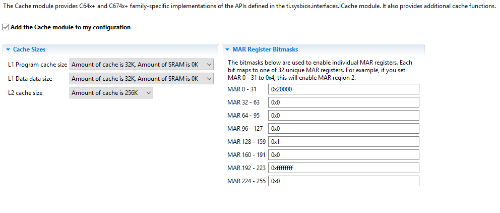
  • Cache is setup via TI RTOS, see below.

    However, I just realized that when we profiled using option #3 (L2 configured 100% RAM), we only changed the platform file to set L2 to 100% RAM.  We never verified that the SYSBIOS Cache page showed L2 set to 100% RAM.  Do we need to do both?

    Profiling the code is done via two functions, see below.

    typedef struct
    {
       U64 CurrentTIme;           /* Delta between start time stamp and end time stamp. */
       U64 CallCount;
       U64 TotalTime;
       volatile U64 AvgTime;      /* Volatile: remove compiler warning, and make sure optimizer doesn't remove the code. */
       U64 MaxTime;
       U64 MinTime;
    } CodeStat_t;
    
    /********************************************************************************************************************************/
    /*  U64 UTI_GetTimeStamp(void))                                                                                                 */
    /*                                                                                                                              */
    /*  This function returns the number of CPU cycles that have executed since power on.                                           */
    /*                                                                                                                              */
    /*  Parameters:                                                                                                                 */
    /*      - none                                                                                                                  */
    /*                                                                                                                              */
    /*  Returns:  number of CPU cycles since power on                                                                               */
    /*                                                                                                                              */
    /*  Notes:  1.  Public API function that can be called from anywhere (HWI, SWI, TASK, or IDLE).                                 */
    /*          2.  This function is thread safe(safely called by multiple TASKs), and reentrant.                                   */
    /********************************************************************************************************************************/
    U64 UTI_GetTimeStamp(void)
    {
       U64 CurrentTicks = 0;
       Types_Timestamp64 BigTicksStamp;
    
       TimestampProvider_get64(&BigTicksStamp);
       CurrentTicks = BigTicksStamp.hi;
       CurrentTicks = CurrentTicks << 32U;
       CurrentTicks = CurrentTicks | BigTicksStamp.lo;
    
       return(CurrentTicks);
    }
    
    
    /********************************************************************************************************************************/
    /*  void UTI_ProfileCode(CodeStat_t *p_CodeStat)                                                                                */
    /*                                                                                                                              */
    /*  This function assists in profiling a block of code by calculating average, min, and max CPU cycles.  Meant to be used with  */
    /*  UTI_GetTimeStamp() to load CurrentTime.  Typical usage described below.                                                     */
    /*                                                                                                                              */
    /*  start = UTI_GetTimeStamp();                                                                                                 */
    /*  ...                                                                                                                         */
    /*  ... block of code you want to profile                                                                                       */
    /*  ...                                                                                                                         */
    /*  end = UTI_GetTimeStamp();                                                                                                   */
    /*  HwiCode.CurrentTime = end - start;                                                                                          */
    /*  UTI_ProfileCode(&HwiCode);                                                                                                  */
    /*                                                                                                                              */
    /*  The initialization of the CodeStat_t structure should be as follows:                                                        */
    /*  static CodeStat_t HwiCode = {0,0,0,0,0,0xFFFFFFFF};                                                                         */
    /*                                                                                                                              */
    /*  Parameters:                                                                                                                 */
    /*      - p_CodeStat:  pointer to the structure that contains all the code profiling information.                               */
    /*                                                                                                                              */
    /*  Returns:  None                                                                                                              */
    /*                                                                                                                              */
    /*  Notes:  1.  Public API function that can be called from anywhere (HWI, SWI, TASK, or IDLE).                                 */
    /*          2.  This function is thread safe(safely called by multiple TASKs), and reentrant.                                   */
    /********************************************************************************************************************************/
    void UTI_ProfileCode(CodeStat_t *p_CodeStat)
    {
       if( p_CodeStat->CurrentTIme > p_CodeStat->MaxTime )
       {
          p_CodeStat->MaxTime = p_CodeStat->CurrentTIme;
       }
    
       if( p_CodeStat->CurrentTIme < p_CodeStat->MinTime )
       {
          p_CodeStat->MinTime = p_CodeStat->CurrentTIme;
       }
    
       p_CodeStat->CallCount++;
       p_CodeStat->TotalTime = p_CodeStat->TotalTime + p_CodeStat->CurrentTIme;
       p_CodeStat->AvgTime = p_CodeStat->TotalTime / p_CodeStat->CallCount;
    }
    

    I'm sure cache eviction is occurring.  This is a fairly large project, multiple TASKs, (5) HWIs, (5) SWIs.  The HWIs execute in the hundreds of cycles range (200-500), the SWI's execute in the hundred thousand cycle range (300000).  On my DSP running at 375MHz, a typical HWI takes 1.5uS to 2.5uS to execute.  The SWI takes around 1mS.  Since I'm sure cache eviction is occurring, that is why I'm attempting to place the HWI and SWI in the "best" memory, so when the cache controller has to refresh L1P, the fewest cycles are wasted.

    - Dean

  • The MAR bit setting for MAR128 and MAR192-MAR223 indicate that the SHRAM and DDR regions are cached as expected.  I would check to confirm when L2 is configured as SRAM in platform configuration. there is information in the platform settings that doesn`t physically change anything on the chip like the CPU frequency.  The platform is only a way to inform BIOS Of the platform settings and not necessarily something that updates the core configuration. 

    The BIOS profiling uses on chip timers but also requires BIOS cpu freq to be set correctly as explained here:

    http://processors.wiki.ti.com/index.php/Processor_SDK_RTOS:_TI_RTOS_Tips_And_Tricks#How_to_get_accurate_clock_ticks_from_the_clock_module.3F

    Make sure you have set the cpuFreq to 375 since the defaults assume 300 Mhz. yOu can also use DSP internal cycles counter TSCL and TSCH just to correlate the data is accurate. 

    Regards,

    Rahul

  • A lot of what you said confuses me.

    1.  Our platform file defines the cache  ..and..  sets the CPU frequency.  Our project uses the SYSBIOS function TimestampProvider_getFreq(), which in turn calls BIOS_getCpuFreq(), which returns 375MHz.  This is what we have set in our platform file.  We've never had to add BIOS.cpuFreq.lo to our SYSBIOS config file.  That seems to be outdated documentation.

    2.  Not sure why you think BIOS profiling uses chip timers.  Our project uses the SYSBIOS function TimestampProvider_get64(), which reads the TSCL and TSCH registers directly.

    3.  I did confirm that when we change the platform file from 100% L2 cache to 100% L2 SRAM,  The SYSBIOS cache module (viewed via XGCONF) shows L2 as all SRAM.

    4.  I can confirm we have to manually add the Timer.intFreqs[0].lo = 25000000; line to our SYSBIOS config file.  It is very frustrating that SYSBIOS can't figure out a where to pick up the input frequency and just assumes you are running on a EVM board loaded with a 24MHz crystal.  Maybe add that to the platform file?  The fact this little nugget of information isn't in the SYSBIOS users guide, and hidden on some wiki link is beyond me.  Lets not focus on this issue, and get back to why the profiling numbers for DDR2 are the best.

    Thanks, Dean

  • Bump.  I realize last week a lot of people were off around July 4th.  However, this week should be "normal", and yet I've heard nothing for 3 days.

    - Dean

  • Hi Dean,

    A few thoughts on the topic:

    1. When doing your measurements, were interrupts disabled?  In other words, are you certain that there aren't any pre-emptions happening within the measured time?  That would certainly throw off the measurements.
    2. In general, I expect DDR2 and the On-Chip RAM to perform fairly similarly (at least on this specific device).  How close were your benchmarks for #1 and #2?  Keep in mind there's going to be some amount of fluctuation simply due to where things get linked in memory and whether there happens to be a cache conflict with something else.
    3. Have you looked into configuring the L2 as 128KB of cache?  Is there still enough room for your HWI's and SWI's with 128KB of L2 SRAM?

    Best regards,
    Brad

  • Answers to your questions from above.

    1.  When profiling HWI code, there are no pre-emptions happening.  We unchecked the box in SYSBIOS for "Enable Interrupt nesting".  The way we understand what happens when that option is NOT checked, is HWI's can't interrupt HWI's.  Basically once a HWI fires, SYSBIOS doesn't re-enable interrupts until AFTER our HWI ISR has run.  When profiling SWI code, HWI's are running.

    2.  100% cache with DDR2 and L3 RAM are close.  Below are the results for one of our HWI's, and one of our SWI's.  We've run dozens of profiling sessions, and let the code run for many thousands of execution passes.  DDR2 code always wins, never loses.

    HWI DDR2:  Average = 280 cycles  (Min=266, Max=680)

    HWI L3 RAM:  Average = 295 cycles  (Min=278, Max=710)

    HWI L2 RAM:  Average = 388 cycles  (Min=280, Max=1475)

    SWI DDR2:  Average = 261,914 cycles  (Max=462,017)

    SWI L3 RAM:  Average = 313,081 cycles  (Max=464,784)

    SWI L2 RAM:  Average = 357,476 cycles  (Max=813,019)

    3.  This violates silicon errata 2.3.17 (SDMA activity can corrupt L1D when L2 is configured as mixed cache/SRAM).  We can't use the --c64p_dma_l1d_workaround as we have too many 3rd party software libraries.  They would all need to be compiled with this switch (none of them are).  We use the simplest workaround:  either L2 is 100% cache or 100% RAM.

    Thanks, Dean

  • Dean Hofstetter said:
    We've run dozens of profiling sessions, and let the code run for many thousands of execution passes.

    I'm referring to program code layout.  This would only be impacted by shuffling around the location to which code is being linked.  

    Dean Hofstetter said:

    SWI DDR2:  Average = 261,914 cycles  (Max=462,017)

    SWI L3 RAM:  Average = 313,081 cycles  (Max=464,784)

    SWI L2 RAM:  Average = 357,476 cycles  (Max=813,019)

    The one that I'm really struggling to understand is your SWI L2 RAM benchmark.  That's only being pre-empted by other SWIs/HWIs that are also in L2 right?

    Dean Hofstetter said:
    This violates silicon errata 2.3.17 (SDMA activity can corrupt L1D when L2 is configured as mixed cache/SRAM). 

    Not true.  This errata relates to data.  If you're placing only code in the L2 SRAM then this errata is not applicable.  Furthermore, even if you put data in this area, as long as only the CPU accesses the data (i.e. not touched by EDMA, USB, Ethernet, etc.), then that is also ok.  The "SDMA" (Slave DMA) interface relates to external masters (like EDMA, USB, etc.) updating the DSP's internal memory.

  • For the "SWI L2 RAM" numbers, all HWI and SWI code is loaded into L2 RAM.  This particular SWI is only getting interrupted by HWI's (it is the highest priority SWI in the system).

    Are there any MAR bits that need to be set if L2 is configured for RAM?  The way I'm reading the data sheet, the answer is no.

    Thanks for pointing out I wasn't understanding silicon errata 2.3.17 correctly.  I don't see the point in trying L2 setup as half cache / half RAM until I understand why 100% RAM yields the worst numbers.

    Thanks, Dean

  • Dean Hofstetter said:
    Are there any MAR bits that need to be set if L2 is configured for RAM?  The way I'm reading the data sheet, the answer is no.

    From your screenshot of your cfg file earlier, it looks like MAR17 is already set.  You could double check through a memory window to be certain.  MAR17 is located at address 0184 8044h.  MAR17 relates to the range of addresses 1100 0000h - 11FF FFFFh.  It might be interesting to check if performance gets worse with MAR17 disabled.

  • According to the C674x Cache Users Guide, L1P accesses are ALWAYS cached (doesn't depend on MAR bits).  It also says L2 RAM addresses are always cached for L1P and L1D (again MAR bits aren't used).

    I assume L1P and L1D are clocked at the CPU frequency (which in my case is 375MHz).  I know that L3 Shared RAM is clocked at half that speed, so that would be 187.5MHz.  I'm not sure what the clock is for L2 RAM.  Can't find that anywhere?  Our DDR2 interface is clocked at 150MHz, and we use the full 16bit bus.

    I'm sure my profiling numbers are correct, but nothing makes sense.  When L2 has a cache miss, if the code is stored in L3 (clocked at half CPU) that has to be faster than DDR2 clocked at 150MHz.  Furthermore, the bus width to L3 must be larger than 16bits, so more data can be moved in a clock cycle.  What am I missing?

    - Dean

  • Dean Hofstetter said:
    According to the C674x Cache Users Guide, L1P accesses are ALWAYS cached

    Great point.  Agreed.

    Dean Hofstetter said:
    I assume L1P and L1D are clocked at the CPU frequency (which in my case is 375MHz). 

    Correct.

    Dean Hofstetter said:
    I know that L3 Shared RAM is clocked at half that speed, so that would be 187.5MHz.

    Although the RAM runs at that speed, there are two switches, a bridge, and a memory protection unit between the DSP and the Shared RAM (same for DDR2).

    Dean Hofstetter said:
    I'm not sure what the clock is for L2 RAM.

    L2 runs as CPU/2.

    Dean Hofstetter said:
    When L2 has a cache miss, if the code is stored in L3 (clocked at half CPU) that has to be faster than DDR2 clocked at 150MHz.

    Our own benchmarks agree that on this particular device, the speed to access L3 and DDR2 are approximately the same.

  • For starters it might be good if we focus on the HWI case since that one is better understood due to the fact that there is no pre-emption.  When you tested the HWI's in L2 SRAM, did you corresponding allocate the HWI_dispatcher in L2 SRAM?

  • For all our test cases, the following code was moved:

    1.  All our HWI code

    2.  All our SWI code

    3.  The .vecs section

    4.  All the SYSBIOS code.

    Below is a snippet from our linker command file that moved code around.

    HWI_CODE : {} > IRAM
    SWI_CODE : {} > IRAM
    .vecs : {} > IRAM
    SYSBIOS_CODE : {-lsysbios.ae674(.text), -lRackCardC6000_pe674.oe674(.text)} > IRAM

    I had a summer intern run these numbers, and on Monday I tried to reproduce what he found.  I have some questions regarding the data I'm seeing vs. what the summer intern found.  I also wanted to experiment with L2 configured as 50% cache and 50% RAM.  I'm out most of this week, so won't be able to get back to this until next week.

    - Dean

  • I had time today to go back and run numbers again.  For each configuration, I let the code execute for over 1 hour.  It resulted in 500,000+ data points.  The numbers below are for a HWI interrupt, nothing can preempt it.

    Code in DDR2 (L1 and L2 all cache):  Avg = 203, Min = 197, Max = 348

    Code in L3 (L1 and L2 all cache):  Avg = 198, Min = 185, Max = 431

    Code in L2 (L1 all cache, L2 128k cache and 128k RAM):  Avg = 214, Min = 186, Max = 597

    DDR2 and L3 are basically a coin flip, however I would select DDR2 based on consistency.  L2 (IRAM) is still the worst option, and I think that now makes sense to me.

    By choosing L2 IRAM I had to cut my L2 cache in half.  Therefore I've increased my chance of having a cache miss in L2.  Furthermore I assume even though the code is in L2 IRAM, when a program cache miss occurs in both L1P and L2, it will copy the code lines from IRAM into L2 cache (and L1P cache).  Basically the cache controller isn't smart enough to say "missed in L1P, but there it is in IRAM, just copy to L1P no need to put it in L2 cache".  So whenever there is a L2 cache miss, there has to be memory copy from somewhere to L2 cache.  Remember, this a a fairly large program.  Many HWI's, SWI's, and TASK's.  I'm sure the L2 cache is getting worked hard, and when I cut it in half, I made things worse (more cache misses, more stalls).

    I'm still scratching my head a little bit on why L3 doesn't significantly out perform DDR2.  Perhaps it is due to the special nature of the L3 memory.  I'm pretty sure I read something about memory accesses to L3 being atomic.  I know the L3 memory was designed to handshake data back and forth between the ARM core and DSP core.  Our part only has the DSP core, so maybe that memory wasn't really designed to hold code.

    Unless you think I'm missing something, I just going to declare for this project, everything gets loaded in DDR2 and L1 + L2 cache is set to 100%.  Any additional thoughts?

    - Dean

  • Dean Hofstetter said:

    Code in DDR2 (L1 and L2 all cache):  Avg = 203, Min = 197, Max = 348

    Code in L3 (L1 and L2 all cache):  Avg = 198, Min = 185, Max = 431

    Code in L2 (L1 all cache, L2 128k cache and 128k RAM):  Avg = 214, Min = 186, Max = 597

    Your DDR2 and L3 results seem reasonable. Our own testing concurs that DDR2 and L3 performance perform similarly. 

    I continue to be surprised by your L2 benchmark, and I think something is being overlooked.

    Dean Hofstetter said:
    I assume even though the code is in L2 IRAM, when a program cache miss occurs in both L1P and L2, it will copy the code lines from IRAM into L2 cache (and L1P cache).  Basically the cache controller isn't smart enough to say "missed in L1P, but there it is in IRAM, just copy to L1P no need to put it in L2 cache". 

    This information is not correct.  Please look in the C674x Cache User Guide at Table 1-3. L1P Miss Stall Characteristics.  The "stall characteristic" is another way of saying "how many cycles is the CPU delayed due to a miss in the L1P"? You should look at the 0-wait state table and compare the L2 SRAM case against the L2 cache case.  In short, for L2 SRAM you will see somewhere between 0-3 stalls when you experience an L1P miss.  For data that is in L2 cache (i.e. a L1P miss but L2 hit) that number rises to 0-5 stalls.  In short, performance for code stored in L2 SRAM should be a little bit better than the performance obtained when code hits in L2, and of course it will be MUCH better than code that misses in L2.

    Assuming you have correctly allocated all of your code in L2 SRAM as you think for these benchmarks, my suspicion is that there is still DATA that you're accessing that is responsible for the slow performance.  Furthermore, in reducing the size of the L2 cache, the time it takes to access that data actually got worse.  

    Dean Hofstetter said:
    I'm still scratching my head a little bit on why L3 doesn't significantly out perform DDR2. 

    In this particular chip, it is the various bridges and interconnects that dominate the access time.  It is a similar amount of logic for both DDR2 and L3.  Correspondingly they perform similarly.  As a side note, in newer devices you'll generally find that the main ARM core has a direct connection to the DDR controller (i.e. bypasses the interconnect).  That was to avoid the latency you're seeing here.

  • Dean Hofstetter said:
    Unless you think I'm missing something, I just going to declare for this project, everything gets loaded in DDR2 and L1 + L2 cache is set to 100%.  Any additional thoughts?

    In general this is a very good configuration.  There's no effort to maintain or optimize, and performance is very good.  This is a reasonable choice for most applications.

  • For the IRAM configuration, I put the audio data buffers in IRAM as well.  Re-ran the test, and same result.  However, there is additional data memory that this HWI uses that didn't get moved:  system stack and SYSBIOS data.

    I agree that it appears that data memory stalls are preventing my IRAM configuration from out performing my DDR2 configuration.  Makes sense to me.  DDR2 configuration has L2 set to 100% cache, so more code and data can be stored before you have a L2 cache miss.  The IRAM configuration cuts the L2 cache in half, so less code and data can live there.  More chance of a L2 cache miss.

    In summary, it appears for smaller projects, playing around with code / data living in IRAM might provide better performance vs. DDR2.  It all depends on how much stuff can stay in L2 cache (now that it has been cut in half).  For larger projects, maxing out L2 cache seems to be the better choice.  Finally, while it seem intuitive that L3 should out perform DDR2, for this chip that isn't the case.  L3 memory offers no real advantage (except for really small projects that might forgo DDR2 memory all together).

    Thanks for your help.

    - Dean