This thread has been locked.

If you have a related question, please click the "Ask a related question" button in the top right corner. The newly created question will be automatically linked to this question.

RTOS/AM5728: PCIe link status issue

Part Number: AM5728

Tool/software: TI-RTOS

Hello,

We are working on a custom board carrying AM5728 SOM Module from Phytec with following setup,

- Board carries Xilinx Artix-7 connected over PCIe bus (containing FPGA endpoint) to the SOM module

- ARM on AM5728 is used to load DSP firmware using remoteproc method

- DSP firmware running SYS/BIOS enumerates the endpoint using the provided pcie libraries

On the software front,

- Linux 4.9.41 used is for booting is from Phytec GIT-repo (stash.phytec.com/.../browse

- The default device-tree has been updated to disable PCIe Root complex (pcie1_rc, pcie2_phy in am572x-pcm-948.dtsi file) so when lspci is run, we see empty output on command line

- This (pcie root-complex 1) is used on the DSP core for communication with endpoint implemented in FPGA

In this setup, the link training has completed and is in L0 state (0x11). But when we start configuration read for device ID and Vendor ID of Endpoint, the link state changes from L0 state to Link Recovery ready (0x10) and back to L0 state. After some time configuration access stops and link-state is seen to be in Detect-QUITE state (0x0). But on evaluation board with same FPGA, link state will remain in L0 state over entire access.

In a separate run, after link training completion, if we don't do any configuration read access, the link state continues to remain in L0 state on our board.

Can you please help to understand under what circumstances, link state changes from L0 to Link recovery ready state?

thanks--

Somesh

  • Hi,

    It seems to me that you have two kinds of boards:

    • But on evaluation board with same FPGA, link state will remain in L0 state over entire access. 
    • Customer board, configuration access caused the link drop

    What is the difference between two boards? Does FPGA and AM5728 use the same PCIE reference clock? Or two separate 100MHz clock? Without read remote device ID/vendor ID, are you able to do memory access? E.g, In the PCIE DSP driver code, you can setup some outbound access with  regionParams.tlpType      = PCIE_TLP_TYPE_MEM;. 

    Regards, Eric 

  • Hi lding,

    Yes we have two setups,

    1. Working setup - Xilinx Eval board with Artix 7 containing the endpoint implementation connected to TI-AM5728 SOM on Phytec eval board on the PCIe edge connector

    2. Custom board (Non working setup) - Xilinx Artix-7 and AM5728 SOM module on board with PCIe connections in board (no edge connector here)

    Answer to your questions,

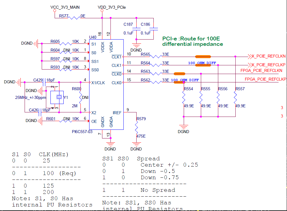
    a> Yes, both FPGA and AM5728 SOM module are supplied with same 100MHz clock from PI6C557-03 chip. Below is the snapshot of our schematic showing the clock supply.

    b> FPGA endpoint contains three bars, BAR-0 & 1. Outbound configuration for both are shown below. Without reading the device-ID or vendor-ID, we are able to write & read back known patterns on the memory in BAR-1, set to 256kB from endpoint. Access to memory also behaves similarly, where after some time, values are read out as 0xFFFF_FFFF instead of written known pattern. Another behavior seen in this case is, endpoint memory address is read out as 0xFFFF_FFFF more quicker if large memory access is done, ie, failure is seen faster when first 1kB words are access when compared to 16words access. After failure, any further access of the memory halts/hangs the DSP (I suppose this part is expected, please confirm). The ltssm state on RC is read out as 0x0 (Detect-quiet) after this failure is seen, I suppose link is down then.

    Below is the outbound configurations on Root-complex.

    --

    pcieAtuRegionParams_t regionParams;


    #define PCIE_WINDOW_CFG_BASE 0x00001000U
    #define PCIE_WINDOW_CFG_MASK 0x00000FFFU

    /*Configure OB region for remote configuration access space*/
    regionParams.regionDir = PCIE_ATU_REGION_DIR_OUTBOUND;
    regionParams.tlpType = PCIE_TLP_TYPE_CFG;
    regionParams.enableRegion = 1;

    regionParams.lowerBaseAddr = PCIE_WINDOW_CFG_BASE;
    regionParams.upperBaseAddr = 0; /* only 32 bits needed given data area size */
    regionParams.regionWindowSize = PCIE_WINDOW_CFG_MASK;

    regionParams.lowerTargetAddr = 0U;
    regionParams.upperTargetAddr = 0U;

    Pcie_atuRegionConfig(handle, pcie_LOCATION_LOCAL, (uint32_t)0U, &regionParams)) != pcie_RET_OK);

    #define PCIE_WINDOW_MEM_MASK 0x000FFFFFU

    //BAR-0 OB configuration

    regionParams.regionDir = PCIE_ATU_REGION_DIR_OUTBOUND;

    regionParams.tlpType = PCIE_TLP_TYPE_MEM;
    regionParams.enableRegion = 1;

    regionParams.lowerBaseAddr = 0x01000000U;
    regionParams.upperBaseAddr = 0; /* only 32 bits needed given data area size */
    regionParams.regionWindowSize = 0x4000U;//16kB FPGA space

    regionParams.lowerTargetAddr = 0xFE400000U;
    regionParams.upperTargetAddr = 0x0U;

    Pcie_atuRegionConfig(handle, pcie_LOCATION_LOCAL, (uint32_t)1U, &regionParams);

    //BAR-1 OB configuration

    regionParams.regionDir = PCIE_ATU_REGION_DIR_OUTBOUND;
    regionParams.tlpType = PCIE_TLP_TYPE_MEM;
    regionParams.enableRegion = 1;

    regionParams.lowerBaseAddr = 0x02000000U;
    regionParams.upperBaseAddr = 0; /* only 32 bits needed given data area size */
    regionParams.regionWindowSize = 0x40000U;//256kB memory space

    regionParams.lowerTargetAddr = 0xFE500000U;
    regionParams.upperTargetAddr = 0x0U;

    Pcie_atuRegionConfig(handle, pcie_LOCATION_LOCAL, (uint32_t)2U, &regionParams);

    --

    Please let me know if I am missing anything here.

    thanks--

    Somesh

  • Hi,

    Thanks for the info! The code looks good. BAR0 is configure access, and BAR 1 and BAR 2 are memory access. With PCIE traffic, you got link failure (reading memory back as 0xFFFF_FFFF meant link failed) and DSP hang is expected.

    This points to some HW issue where the PCIE link is not stable under traffic. In the schematic, I saw "X" for PCIE_REFCLKN/P, does it mean un-connected? can you clarify:

    • In working setup, AM5728 got the PCIE clock from PI6C557-03 (CLK1)? And FPGA got the clock from FPGA_PCIE_REFCLKN/P (CLK0),  will the PCIE edge connector also pass the clock from RC to EP? Or the edge connector only passing the PCIE data lane? 
    • What about the failure setup? When you have the direct PCIE connection, do you also connect the PCIE clock signal or only the PCIE data lane?

    Regards, Eric    

  • Hi Eric,

    Below are answer to your questions,

    1. In the schematic, I saw "X" for PCIE_REFCLKN/P, does it mean un-connected? can you clarify:

    [Somesh] The 'X' is naming convention to differentiate signals going into FPGA v/s AM5728 SOM module ('X' is used for signals to AM5728).

    2. In working setup, AM5728 got the PCIE clock from PI6C557-03 (CLK1)? And FPGA got the clock from FPGA_PCIE_REFCLKN/P (CLK0),

    [Somesh] Yes, X_PCIE_REFCLKN/X_PCIE_REFCLKP is connected to AM5728 and FPGA_PCIE_REFCLKN/FPGA_PCIE_REFCLKP goes to FPGA clock

    3. Will the PCIE edge connector also pass the clock from RC to EP? Or the edge connector only passing the PCIE data lane?

    [Somesh] Yes, the AM5728 eval board passes both the clock and data lane on the edge connector (this is the working setup).

    4. What about the failure setup? When you have the direct PCIE connection, do you also connect the PCIE clock signal or only the PCIE data lane?

    [Somesh] On the custom board, we do not have edge connector, both RC (AM5728) and EP (FPGA) are on board and connected directly. Both PCIe clock signal and data lanes are connected.

    Below are the lane lengths on our custom board (in mils),

    X_PCI_RXP0 - 1494

    X_PCI_RXN0 - 1492

    X_PCI_TXP0 - 1535

    X_PCI_TXN0 - 1534

    Above two pairs are data lanes between RC (AM5728) and EP (FPGA)

    FPGA_PCI_REFCLKP0 - 1882

    FPGA_PCI_REFCLKN0 - 1881

    X_PCI_REFCLKP0 - 702

    X_PCI_REFCLKN0 - 672

    Above two clock pairs are from clock-generator (PI6C557-03) to FPGA (CLK-0) and AM5728 (CLK-1) as shown in schematic snippet.

    Please let me know if you need more info and if we are missing anything.

    thanks--

    Somesh

  • Thanks,

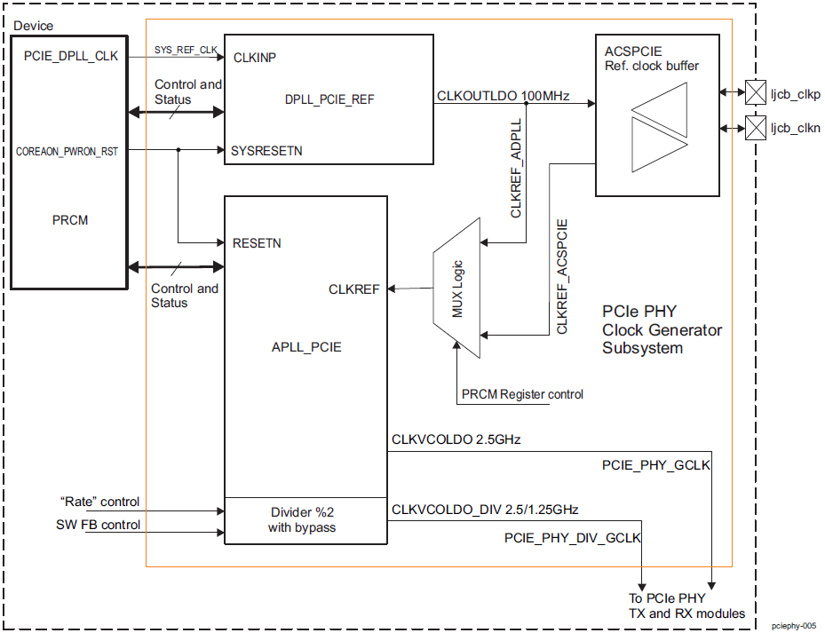
    In the pcie_sample_board.c there is a code to select the clock source:

    HW_SET_FIELD(regVal, CM_CLKMODE_APLL_PCIE_REFSEL,
    CM_CLKMODE_APLL_PCIE_REFSEL_CLKREF_ADPLL);

    You may try to see if change to:

    HW_SET_FIELD(regVal, CM_CLKMODE_APLL_PCIE_REFSEL,
    CM_CLKMODE_APLL_PCIE_REFSEL_CLKREF_ACSPCIE);

    helps or not.

    The PCIE link instability under traffic is mostly HW issue (reference clock, board design, etc). I also added our HW engineer for help.

    Regards, Eric

  • Please provide the 'LSPCI -VV" logs for pre and post error conditions on your custom board.

  • Hi Eric,

    I dug into some details of the register programming you asked me to update/check. Found below block diagram in TRM explaining it.

    This is exactly what I wanted. Current programming selects CLKREF_ADPLL, but we need RC to run on CLKREF_ACSPCIE. With this programming update the memory access on the enumerated endpoint runs without any link failures (ran around 3 - 4 times for ~30mins). The suspect now is on, how stable CLKREF_ADPLL clock generated from PCIE_DPLL_CLK and how is the eval-setup (working setup) managing to communicate with CLKREF_ADPLL. But for now this solves my problem.

    I have a few more related questions and will open a new thread for this. Thanks for your inputs and support Eric.

    --Somesh