


Part Number: AM3358
Other Parts Discussed in Thread: TMDXEVM3358, TPS51200
Hello.
I have newly designed a custom board based on TMDXEVM3358 (AM3358 GP ?).
I removed unnecessary parts and changed DDR3 RAM.
The main parts are as blows.
1. MPU : AM3358BZCZ80
2. RAM : MT41K512M8DA107AITP, 2ea,
https://www.micron.com/products/dram/ddr3-sdram/part-catalog/mt41k512m8da-107-it
3. Flash : MT29F2G08ABAEAH4, 1ea
I applied MT41K512M8DA-107 as a DDR3 RAM instead of MT41K512M8DA-125 in the TMDXEVM3358.
I had been trying to interface DDR3 as explained in the tutorials below:
http://processors.wiki.ti.com/index.php/AM335x_EMIF_Configuration_tips
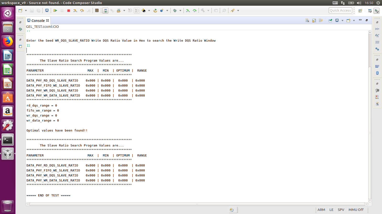
When I run the 'DDR3_slave_ratio_search_auto.out', I have always got 0x00 for console output. ( attached it blow)
And I had tried to modify the momory value between 0x80000000 and 0xBFFFFFFF, value didn't stick and kept changing.
I tried to change Ratio speed and register value, but it kept showing same result(0x00).
I would like to attach some files for your review.
1. GEL file
2. Connection Log file by using above GEL file
CortxA8: Output: ****  AM335x EVM v1.5 Initialization is in progress ..........

CortxA8: Output: ****  AM335x ALL PLL Config for ispark :: OPP == OPP100 is in progress .........

CortxA8: GEL Output: GetInputClockFrequency() :: RD_MEM_32(CONTROL_STATUS) :: 0x00400302

CortxA8: GEL Output: PIN 15 14 :: Clock = 0x00000001

CortxA8: GEL Output: PIN 13 12 :: Should be 0 = 0x00000000

CortxA8: GEL Output: PIN 11 10 :: Mux = 0x00000000

CortxA8: GEL Output: PIN 9     :: ECC ROM = 0 :: Don't Care = 0x00000000

CortxA8: GEL Output: PIN 8     :: Nand Bus Width = 0x00000000

CortxA8: GEL Output: PIN 7  6  :: MII == 00 :: = 0x00000000

CortxA8: GEL Output: PIN 5     :: Clock Out = 0x00000000

CortxA8: GEL Output: SysBoot[4:0] = 0x00000002

CortxA8: Output: Input Clock Read from SYSBOOT[15:14]:  24MHz.

CortxA8: Output: ****  Going to Bypass...

CortxA8: Output: ****  Bypassed, changing values...

CortxA8: Output: ****  Locking ARM PLL

CortxA8: Output: ****  Core Bypassed

CortxA8: Output: ****  Now locking Core...

CortxA8: Output: ****  Core locked

CortxA8: Output: ****  DDR DPLL Bypassed

CortxA8: Output: ****  DDR DPLL Locked

CortxA8: Output: ****  PER DPLL Bypassed

CortxA8: Output: ****  PER DPLL Locked

CortxA8: Output: ****  DISP PLL Config is in progress ..........

CortxA8: Output: ****  DISP PLL Config is DONE ..........

CortxA8: Output: ****  AM335x ALL ADPLL Config for ispark :: OPP == OPP100 is Done .........

CortxA8: Output: ****  AM335x DDR3 EMIF and PHY configuration is in progress.........

CortxA8: Output: EMIF PRCM is in progress .......

CortxA8: Output: EMIF PRCM Done

CortxA8: Output: DDR PHY Configuration in progress

CortxA8: Output: Waiting for VTP Ready .......

CortxA8: Output: VTP is Ready!

CortxA8: Output: DDR PHY CMD0 Register configuration is in progress .......

CortxA8: Output: DDR PHY CMD1 Register configuration is in progress .......

CortxA8: Output: DDR PHY CMD2 Register configuration is in progress .......

CortxA8: Output: DDR PHY DATA0 Register configuration is in progress .......

CortxA8: Output: DDR PHY DATA1 Register configuration is in progress .......

CortxA8: Output: Setting IO control registers.......

CortxA8: Output: EMIF Timing register configuration is in progress .......

CortxA8: Output: EMIF Timing register configuration is done .......

CortxA8: Output: PHY is READY!!

CortxA8: Output: DDR PHY Configuration done

CortxA8: Output: ****  AM335x EVM v1.5 Initialization is Done ******************
3. .AM335x_DDR_register_calc_tool.xls
MT41K512M8RH-107E.AM335x_DDR_register_calc_tool.xls
4. RatioSeed_AM335x_boards.xls
0647.RatioSeed_AM335x_boards.xls
5. DDR3_slave_ratio_search_screenShot
6. ddr analysis script Log
CONTROL: device_id = 0x2b94402e
  * AM335x family
  * Silicon Revision 2.1

CONTROL: control_status = 0x00400302
  * SYSBOOT[15:14] = 01b (24 MHz)
CM_CLKSEL_DPLL_DDR = 0x00019017
  * DPLL_MULT = 400 (x400)
  * DPLL_DIV = 23 (/24)
CM_DIV_M2_DPLL_DDR = 0x00000201
  * CLKST = 1: M2 output clock enabled
  * DIVHS = 1 (/1)

DPLL_DDR Summary
 -> F_input = 24 MHz
 -> CLKOUT_M2 = DDR_PLL_CLKOUT = 400 MHz

EMIF: SDRAM_CONFIG = 0x61c04bb2
  * Bits 31:29 (reg_sdram_type) set for DDR3
  * Bits 28:27 (reg_ibank_pos) set to 0
  * Bits 26:24 (reg_ddr_term) set for RZQ/4 (001b)
  * Bits 22:21 (reg_dyn_odt) DDR3 dynamic ODT set to RZQ / 2
  * Bit  20    (reg_ddr_disable_dll) set to 0, DDR3 DLL enabled
  * Bits 19:18 (reg_sdram_drive) set for RZQ/6 (00b)
  * Bits 17:16 (reg_cwl) set for 0, CWL = 5
  * Bits 15:14 (reg_narrow_mode) set to 1 -> 16-bit EMIF interface
  * Bits 13:10 (reg_cl) set to 2 -> CL = 5
  * Bits 09:07 (reg_rowsize) set to 7 -> 16 row bits
  * Bits 06:04 (reg_ibank) set to 3 -> 8 banks
  * Bits 02:00 (reg_pagesize) set to 2 -> 10 column bits

EMIF: PWR_MGMT_CTRL = 0x00000000
 * Bits 10:8 reg_lp_mode set to 0, auto power management disabled
 * Warning: Bits 7:4 (reg_sr_tim) are in violation of Maximum Self-Refresh Command Limit
   -> Please see the silicon errata (DDR3: JEDEC Compliance for Maximum Self-Refresh Command Limit) for more details.
   -> This is only an issue if used in conjunction with reg_lp_mode=2.

DDR PHY: DDR_PHY_CTRL_1 = 0x00000007
  * WARNING: reg_phy_enable_dynamic_pwrdn disabled.
  * Bits 9:8 (reg_phy_rd_local_odt) to 0 -> no termination
    -> Read termination is highly recommended in general for best DDR3 signal integrity
  * Bits 4:0 (reg_read_latency) set to 7 -> Ok: CL+2 is typical with PHY_INVERT_CLKOUT=1.

*********************
*** Register Dump ***
*********************

*(0x4c000000) = 0x40443403
*(0x4c000004) = 0x40000004
*(0x4c000008) = 0x61c04bb2
*(0x4c00000c) = 0x00000000
*(0x4c000010) = 0x00000c30
*(0x4c000014) = 0x00000c30
*(0x4c000018) = 0x0aaad4db
*(0x4c00001c) = 0x0aaad4db
*(0x4c000020) = 0x2e6b7fda
*(0x4c000024) = 0x2e6b7fda
*(0x4c000028) = 0x501f867f
*(0x4c00002c) = 0x501f867f
*(0x4c000038) = 0x00000000
*(0x4c00003c) = 0x00000000
*(0x4c000054) = 0x00ffffff
*(0x4c000058) = 0x8000140a
*(0x4c00005c) = 0x00021616
*(0x4c000080) = 0x00000000
*(0x4c000084) = 0x00000000
*(0x4c000088) = 0x00010000
*(0x4c00008c) = 0x00000000
*(0x4c000090) = 0x32d55e03
*(0x4c000098) = 0x00050000
*(0x4c00009c) = 0x00050000
*(0x4c0000a4) = 0x00000000
*(0x4c0000ac) = 0x00000000
*(0x4c0000b4) = 0x00000000
*(0x4c0000bc) = 0x00000000
*(0x4c0000c8) = 0x50074be4
*(0x4c0000d4) = 0x00000000
*(0x4c0000d8) = 0x00000000
*(0x4c0000dc) = 0x00000000
*(0x4c0000e4) = 0x00000007
*(0x4c0000e8) = 0x00000007
*(0x4c000100) = 0x00000000
*(0x4c000104) = 0x00000000
*(0x4c000108) = 0x00000000
*(0x4c000120) = 0x00000305

************************
*** IOCTRL Registers ***
************************

CONTROL: DDR_CMD0_IOCTRL = 0x0000018b
  * ddr_ba2 Pullup/Pulldown disabled
  * ddr_wen Pullup/Pulldown disabled
  * ddr_ba0 Pullup/Pulldown disabled
  * ddr_a5 Pullup/Pulldown disabled
  * ddr_ck Pullup/Pulldown disabled
  * ddr_ckn Pullup/Pulldown disabled
  * ddr_a3 Pullup/Pulldown disabled
  * ddr_a4 Pullup/Pulldown disabled
  * ddr_a8 Pullup/Pulldown disabled
  * ddr_a9 Pullup/Pulldown disabled
  * ddr_a6 Pullup/Pulldown disabled
  * Bits 9:5 control ddr_ck and ddr_ckn
    - Slew slow
    - Drive Strength 9 mA
  * Bits 4:0 control ddr_ba0, ddr_ba2, ddr_wen, ddr_a[9:8], ddr_a[6:3]
    - Slew slow
    - Drive Strength 8 mA
CONTROL: DDR_CMD1_IOCTRL = 0x0000018b
  * ddr_a15 Pullup/Pulldown disabled
  * ddr_a2 Pullup/Pulldown disabled
  * ddr_a12 Pullup/Pulldown disabled
  * ddr_a7 Pullup/Pulldown disabled
  * ddr_ba1 Pullup/Pulldown disabled
  * ddr_a10 Pullup/Pulldown disabled
  * ddr_a0 Pullup/Pulldown disabled
  * ddr_a11 Pullup/Pulldown disabled
  * ddr_casn Pullup/Pulldown disabled
  * ddr_rasn Pullup/Pulldown disabled
  * Bits 4:0 control ddr_15, ddr_a[12:10], ddr_a7, ddr_a2, ddr_a0, ddr_ba1, ddr_casn, ddr_rasn
    - Slew slow
    - Drive Strength 8 mA
CONTROL: DDR_CMD2_IOCTRL = 0x0000018b
  * ddr_cke Pullup/Pulldown disabled
  * ddr_resetn Pullup/Pulldown disabled
  * ddr_odt Pullup/Pulldown disabled
  * ddr_a14 Pullup/Pulldown disabled
  * ddr_a13 Pullup/Pulldown disabled
  * ddr_csn0 Pullup/Pulldown disabled
  * ddr_a1 Pullup/Pulldown disabled
  * Bits 4:0 control ddr_cke, ddr_resetn, ddr_odt, ddr_csn0, ddr_[a14:13], ddr_a1
    - Slew slow
    - Drive Strength 8 mA
CONTROL: DDR_DATA0_IOCTRL = 0x0000018b
  * ddr_d8 Pullup/Pulldown disabled
  * ddr_d9 Pullup/Pulldown disabled
  * ddr_d10 Pullup/Pulldown disabled
  * ddr_d11 Pullup/Pulldown disabled
  * ddr_d12 Pullup/Pulldown disabled
  * ddr_d13 Pullup/Pulldown disabled
  * ddr_d14 Pullup/Pulldown disabled
  * ddr_d15 Pullup/Pulldown disabled
  * ddr_dqm1 Pullup/Pulldown disabled
  * ddr_dqs1 and ddr_dqsn1 Pullup/Pulldown disabled
  * Bits 9:5 control ddr_dqs1, ddr_dqsn1
    - Slew slow
    - Drive Strength 9 mA
  * Bits 4:0 control ddr_d[15:8], ddr_dqm1
    - Slew slow
    - Drive Strength 8 mA
CONTROL: DDR_DATA1_IOCTRL = 0x0000018b
  * ddr_d0 Pullup/Pulldown disabled
  * ddr_d1 Pullup/Pulldown disabled
  * ddr_d2 Pullup/Pulldown disabled
  * ddr_d3 Pullup/Pulldown disabled
  * ddr_d4 Pullup/Pulldown disabled
  * ddr_d5 Pullup/Pulldown disabled
  * ddr_d6 Pullup/Pulldown disabled
  * ddr_d7 Pullup/Pulldown disabled
  * ddr_dqm0 Pullup/Pulldown disabled
  * ddr_dqs0 and ddr_dqsn0 Pullup/Pulldown disabled
  * Bits 9:5 control ddr_dqs0, ddr_dqsn0
    - Slew slow
    - Drive Strength 9 mA
  * Bits 4:0 control ddr_d[7:0], dqm0
    - Slew slow
    - Drive Strength 8 mA
CONTROL: DDR_IO_CTRL = 0x00000000
  * Bit 31: DDR_RESETn controlled by EMIF.
  * Bit 28 (mddr_sel) configured for SSTL, i.e. DDR2/DDR3/DDR3L operation.
CONTROL: VTP_CTRL = 0x00000067
  * VTP not disabled (expected in normal operation, but not DS0).
CONTROL: VREF_CTRL = 0x00000000
  * VREF supplied externally (typical).
CONTROL: DDR_CKE_CTRL = 0x00000001
  * CKE controlled by EMIF (normal/ungated operation).
I would like to ask you some questions as blows.
1. Can I use micron MT41K512M8DA-107 ?
2. What should I check my board to clear this issue?
=> I have checked PCB Artwork and I didn't find any deviation for the Datasheet 7.7.2 ~ .
=> Should I change the terminal resistor value as fit as my design?
( I use 47R and 49.9R for terminal resistor as same as reference sch on TMDXEVM3358. )
3. Do I make any mistakes for ration/resistor excel sheet?
=> I have changed a lot of times.... but same result.... only 0x00
Thank you in advance.


