This thread has been locked.

If you have a related question, please click the "Ask a related question" button in the top right corner. The newly created question will be automatically linked to this question.

Linux/AM5728: GPMC Wait pin control

Part Number: AM5728

Tool/software: Linux

Hi Champs,

We have two kind of question for wait pin control

1) Wait pin monitor timing

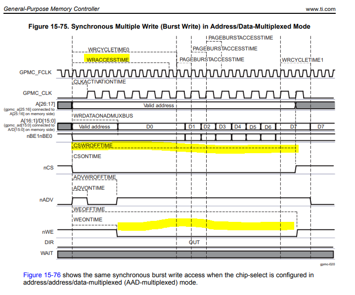
When GPMC read, wait pin monitor timing defined RDACCESSTIME and "GPMC_CONFIG1_i[19:18]. ( in this case, 0x2: start 3clock before  of GPMC_CLK.

On the other hand , when GPMC write it defined WRACCESSTIME and this is fixed value. This monitor start timing in write mode is same as read monitor.

However, we couldn't detect wait pin monitor at write mode.  Because, we didn't understand write access time parameter correctly. 

Could you please tell us correct wait pin monitor at write mode ? 

2) Wait signal 

Currently, we are using two devices at CS0 and CS2. This device need external wait pins.

When we define to use WAIT0 in  CS0 and CS2 at Linux device tree, it occure error.

So, this error due to AM57xx GPMC has two external wait pin and 8CS reasion. 

This mesan, can't we share WAIT0 pin between CS0 and CS2 ?

  • Hi Kaz,

    1)

    Kz777 said:
    Could you please tell us correct wait pin monitor at write mode ? 

    I'm interested to know if the accesses are synchronous or asynch and I need to know the values of WAITMONITORINGTIME and GPMCFCLKDIVIDER for both chip selects.
    If synchronous, I think GPMCFCLKDIVIDER should be equal to 2 so GPMC_FCLK 266MHz / (2+1) = 88.67MHz. If synchronous, I need to know if performing write bursts.

    Can you provide a register dump of GPMC registers including...
    * GPMC_CONFIG
    * CS0 Regs (GPMC_CONFIG1_0, GPMC_CONFIG2_0, GPMC_CONFIG3_0, GPMC_CONFIG4_0, GPMC_CONFIG5_0, GPMC_CONFIG6_0, GPMC_CONFIG7_0)
    * CS2 Regs (GPMC_CONFIG1_2, GPMC_CONFIG2_2, GPMC_CONFIG3_2, GPMC_CONFIG4_2, GPMC_CONFIG5_2, GPMC_CONFIG6_2, GPMC_CONFIG7_2)

    WAIT monitoring is described in TRM sections (www.ti.com/.../spruhz6k.pdf)
    15.4.4.8.3.1 Wait Pin Monitoring Control
    15.4.4.8.3.1.1 Wait Monitoring During Asynchronous Read Access
    15.4.4.8.3.1.2 Wait Monitoring During Asynchronous Write Access
    15.4.4.8.3.1.3 Wait Monitoring During Synchronous Read Access
    15.4.4.8.3.1.4 Wait Monitoring During Synchronous Write Access

    Basically for asynch modes, WAIT needs to be in a valid state 2 GPMC_CLK cycles before WRACCESSTIME (and PAGEBURSTACCESSTIME for a burst/page write). 1 GPMC_CLK cycle is defined as (GPMCFCLKDIVIDER + 1) GPMC_FCLK eventhough the access is asynch and no clock appears on the GPMC_CLK pin. WAITMONITORINGTIME can be non-zero if more delay is required between WAIT inactive and data being latched by the device (during a write).

    For synchronous accesses, WAIT needs to be in a valid state at WRACCESSTIME if WAITMONITORINGTIME = 0.
    Or WAIT needs to be in a valid state WAITMONITORINGTIME x (GPMCFCLKDIVIDER + 1) * GPMC_FCLK cycles before WRACCESSTIME if WAITMONITORINGTIME is not equal to 0
    If write bursts are used, WAITMONITORINGTIME can be equal to 0 only if a clock divider of 3 or 4 (GPMC_CONFIG1_i[1:0] GPMCFCLKDIVIDER = 0x2 or 0x3).

    2) Can 2 GPMC chip selects share the same wait pin? Linux device tree shows an error.

    I believe the GPMC peripheral can allow 2 chip selects to share a single WAIT pin input.
    It is not possible for two GPMC chip selects to be active simultaneously, so each chip select will monitor the single WAIT pin when it has access to the GPMC pins.
    What is the error you are seeing? I suspect it might be due to the GPMC driver, but I am not sure.

    Regards,
    Mark

  • Hi Mark,

    Thanks for your help. 

    Actually, we could fix this GPMC issue.

    So, Please confirm one more thing.

    Customer read some article about GPMC (Not TI e2e or AM57 document) at write mode.

    "WRACCESSTIME " have to set small value than CSWROFFTIME and WEOFFTIME.

    This doesn't depend on Async or sync.

    Then, they could fix this issue.

    However, we would like to confirm if this restriction is correct. 

    According to this parameter WRACCESSTIME seems smaller than CSWROFFTIME and WEOFFTIME.

    However, there is no comment for this restriction.

    Do we have such a restriction ?

  • Hi Mark,

    Could you please have a comment on this ?

  • Hi Kaz-san,

    For synchronous writes, WRACCESSTIME needs to be set to the rising edge of GPMC_FCLK corresponding to the rising edge of GPMC_CLK when the memory device latches the incoming data driven on the data bus by the GPMC. nWE needs to have already been asserted low when this rising edge of GPMC_CLK occurs. And nWE needs to remain low for the CLK-to-nWE hold time requirement specified in the datasheet of the memory device.

    For asynch memories, usually the nWE signal rising edge is used as the latching event for data being written by the GPMC. In this case, I believe WRACCESSTIME and WEOFFTIME might be the same.
    If the memory provides a signal to the WAIT pin, WrAccessTime is used as a WAIT invalid timing window. It must be set to a value such that the WAIT pin is at a valid state two GPMC clock cycle before WrAccessTime.

    In any case, CSWROFFTIME and WRCYCLETIME need to occur after WRACCESSTIME and nWE deassertion.

    For the figure you attached, there is a text description that states the programmed value of WRCYCLETIME equals WRCYCLETIME0 + WRCYCLETIME1. WRCYCLETIME0 and WRCYCLETIME1 delays are not actual parameters and are only a graphical representation of the full WRCYCLETIME value.

    Regards,
    Mark

  • Hi Mark,

    Sorry, I have some feed back from customer.

    >For asynch memories, usually the nWE signal rising edge is used as the latching event for data being written by the GPMC. In this case, I believe >WRACCESSTIME and WEOFFTIME might be the same.

    -Customer condition set WRACCESS TIME < WEOFFTIME. Then, their application seems working. Do we have to set same value for these parameters ?

    >In any case, CSWROFFTIME and WRCYCLETIME need to occur after WRACCESSTIME and nWE deassertion.

    after WRACCESSTIME and nWE de-assertion, is it able to happen  CSWROFFTIME and WRCYCLETIME after 1cycle later ?

  • Hi Kaz-san,

    Kz777 said:
    -Customer condition set WRACCESS TIME < WEOFFTIME. Then, their application seems working. Do we have to set same value for these parameters ?

    This is fine. WRACCESSTIME does not NEED to be the same as WEOFFTIME. The data will remain on the GPMC data bus until WRCYCLETIME completes.
    It is more important for the WAIT signal - Is the customer using the WAIT signal?

    Kz777 said:
    after WRACCESSTIME and nWE de-assertion, is it able to happen  CSWROFFTIME and WRCYCLETIME after 1cycle later ?

    Yes, this is permissible. The GPMC section Read Cycle Time and Write Cycle Time (RDCYCLETIME / WRCYCLETIME) in the TRM specifies...
    "When RDCYCLETIME or WRCYCLETIME completes, if they are not already deasserted, all control signals (nCS, nADV/ALE, nOE/RE, nWE, and BE0/CLE) are deasserted to their reset values, regardless of their deassertion time parameters."

    So if CSWROFFTIME occurs at the same time as WRCYCLETIME, the CSn signal will go high/deasserted.

    But I want to make you aware of this wiki that states that CSWROFFTIME must be less than WRCYCLETIME. See Rule 8 here http://processors.wiki.ti.com/index.php/Tips_for_configuring_OMAP35x,_AM35x,_and_AM-DM37x_GPMC_registers

    Sorry I do not have the background about this rule.

    Regards,
    Mark

  • Hi Mark,

    Thank you for reply.

    >This is fine. WRACCESSTIME does not NEED to be the same as WEOFFTIME. The data will remain on the GPMC data bus until WRCYCLETIME completes.
    >It is more important for the WAIT signal - Is the customer using the WAIT signal?

    - Yes, Customer is using "WAIT signal". In this case , do they have to set same value for WRACCESSTIME and WEOFFTIME ?

    Regards,

    Kz777

  • Hi Kaz-san,

    Kz777 said:
    - Yes, Customer is using "WAIT signal". In this case , do they have to set same value for WRACCESSTIME and WEOFFTIME ?

    No, this means that the WRACCESSTIME must occur before WEOFFTIME by enough GPMC_FCLK cycles so that the GPMC_WAIT pin is at a valid state at least 2 GPMC_CLK cycles before WRACCESSTIME completes.

    Note that the period of 1 GPMC_CLK cycle = the period of 1 GPMC_FCLK cycle * (GpmcFCLKDivider + 1).

    Also note that the WRACCESSTIME and WEOFFTIME values are in GPMC_FCLK cycles.

    Regards,
    Mark