This thread has been locked.

If you have a related question, please click the "Ask a related question" button in the top right corner. The newly created question will be automatically linked to this question.

AM1808 PLL seems to be on after reset

Other Parts Discussed in Thread: AM1808

I have a custom board with the AM1808. I'm trying to flash the board using UART2. My BOOTME message is coming out way too fast  on reset. It's 2.31 Mbps instead of 115.2 Kbps.

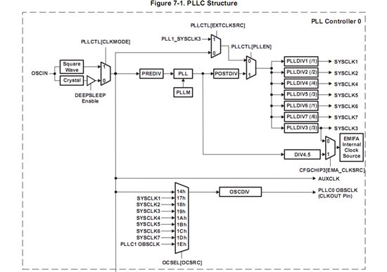
From the Boot loader document sprab41c.pdf I learned that the UART divider is by default 8 and the UART oversampling 13. So normally you get

BAUD = 24MHz/(2 x 13 x 8) = 115384.

However, the default PLLM is 13h which would give a system frequency of 24MHz x 20 = 480 MHz. But it's supposed to be turned off after reset.

However using this value the BAUD would be calculated as:

BAUD = 480 MHz/(2 x 13 x 8) = 2.308 MHz which is what I'm getting. So it appears my PLL is getting enabled on reset. This agrees with the value I used in the UBL to get the correct baud rate there under emulator control. I used the /16 and DLL = 130 to get 480 MHz/(2*16*130) = 115384. But I had to comment out the line of code that (supposedly) takes it out of bypass mode since it causes the emulator to crash.

My question is: Is it possible by some pin set up to enable the PLL on reset? What else could be causing it to be on after reset? I have a reset button and even after power is good the same thing occurs on reset. Power sequencing looks good. I can run good from the emulator but cannot program the PLL under emulator control otherwise it crashes.

Help!

  • John Dehelian said:
    Is it possible by some pin set up to enable the PLL on reset?

    By default, the PLLs come up in bypass mode.  It will ignore the PLLM and PLLDIV values.  Can you verify that PLLCTL[PLLEN] is a value of 0, meaning that the PLL is in bypass mode? 

    John Dehelian said:
    What else could be causing it to be on after reset?

    Are you using CCS?  Can you verify that the GEL file is removed before flashing?  Sometimes the GEL file includes a on-connect function that will initialize and enable the PLLs. 

    Also, can you verify that you set the boot pins to UART2 boot?  If you leave the pins to boot from SPI/NAND flash, it might try to execute the previously loaded image.

    --Christina

  • Thanks for the quick response Christina

    'When I have the debugger connected it does show that it's in bypass mode. However, when I run the UBL V1.65 under the emulator, it crashes at the point where the PLL0 is taken out of bypass mode. So in order to be able to run I've commented out that line. Then the UBL runs as if it were taken out of bypass mode using the default multiplier (as can be deduced from the UART speed with the values used to obtain the 115.2 Kbps). When I first load the debugger I was trying to change the state of the bypass from 0 to 1 using the register view. But it won't show a change.If I run the initialization code in the UBL that changes the multiply and divide registers of the PLL and then manually try to change the bypass mode the emulator crashes as if I had run the code to take it out of bypass mode. I have another posting describing this issue. But now it seems maybe they are related.

    Yes I am using CCS. Currently I don't have any GEL file specified thogh. However when I was using the AM1808.gel it was not executing the clock set up functions.

    There are no images previously loaded. These are boards fresh from the manufacturer, blank chips. There is no SPI or NAND flash on the board only nor. When I start up in Code Composer and look at the BOOTCFG register it shows correctly 0x14. Plus I do see the BOOTME message coming out the UART2 port (even with the debugger detached). It is just coming out too fast. I checked it with an oscilloscope and decoded the ascii string manually. The PLL must be coming up on even with no debugger attached.

    Possibly of note. The chips on the eval board are d800k004 and those on my custom board are d800k006.

    Let me know if you need any other information. I will be working on this until I find a solution.

    John

  • This is an update on my testing so far.

    In the debugger, I'm able to turn on the observation clock OBSCLK and set the OSCDIV to a reasonable value so my 60 MHz oscilloscope can see the signal (programming the it to 19 sets it to 20 which is a good round number) and the output is 24 MHz which means the processor is indeed running at 480 MHz. At this point changing any of the PLL pre dividers, post dividers has no effect. The OSCSEL seems to work with the exception that when set to 0x14 this should be the 24 MHz oscillator. But with this (taking into account theOSCDIV is set to 31) the output is still 480 MHz. Setting it to the other SYSCLKs all makes sense with respect to their default dividers. But again changing those divisors has no effect. I'm thinking that maybe once the PLL is turned on these registers are locked out. The other thing that doesn't make sense is that the PLLCTL shows that the PLL is powered down, reset, and in bypass mode. This doesn't agree with the frequency I'm seeing at the output.


    With nothing in the data sheets to explain this behavior I'm starting to believe that this is a problem with the newer silicon. Is anybody else using the d800k006 silicon? Does anyone have anything I can try?


    I tried the same tests on the evaluation board (Zoom am1808) and they behave as expected. This proves that my debugger is not doing some register manipulation before I'm able to observe it.

  • When you set OSCSEL to 0x14, the output of OBSCLK is equal to the crystal.  It does not show the actual operational speed of the device.  Below is a snapshot (taken from the system reference guide) of how the clocks are connected.  To know how fast the UART is operating at, it will be best to monitor SYSCLK2 since it feeds into the module clock. 


    There is a way to lock the PLL0 MMRs to prevent rogue operations.  Can you check SYSCFG0[CFGCHIP0]?  Is the PLL_MASTER_LOCK set to 0 or 1?  If it is set to 1, then the PLLC0 MMRs are locked, so any changes to the MMRs will be ignored.

    Can you also check SYSCFG0[CFGCHIP3]?  What are the values for PLL1_MASTER_LOCK and ASYNC3_CLKSRC?  UART2 belongs in the ASYNC3 group, so ASYNC3_CLKSRC lets the user choose to source the clock from PLL0 or PLL1. 


    For the setup, are all the custom boards populated with the d800k006 silicon?  Are there any custom boards populated with the older silicon revision?

    --Christina

  • Thanks again for your help Christina. I included responses below after your questions.

    clam said:

    When you set OSCSEL to 0x14, the output of OBSCLK is equal to the crystal.  It does not show the actual operational speed of the device.  Below is a snapshot (taken from the system reference guide) of how the clocks are connected.  To know how fast the UART is operating at, it will be best to monitor SYSCLK2 since it feeds into the module clock. 

    Although it SHOULD show the crystal frequency when set to 0x14 I am seeing 480 MHz with this setting. I did try the SYSCLK2 setting and it shows the frequency divided by 2 as expected. But it's still 240 MHz instead of 12 MHz as would be expected if the PLL were bypassed.


    There is a way to lock the PLL0 MMRs to prevent rogue operations.  Can you check SYSCFG0[CFGCHIP0]?  Is the PLL_MASTER_LOCK set to 0 or 1?  If it is set to 1, then the PLLC0 MMRs are locked, so any changes to the MMRs will be ignored.

    It is set to 0 or FREE. What's curious about my situation is that I can actually change the values of the multiplier and divider register. They just have no effect. I tested this on the eval board and they can be changed while the PLL is operational. If I set it to LOCK then I cannot change the register values.

    Can you also check SYSCFG0[CFGCHIP3]?  What are the values for PLL1_MASTER_LOCK and ASYNC3_CLKSRC?  UART2 belongs in the ASYNC3 group, so ASYNC3_CLKSRC lets the user choose to source the clock from PLL0 or PLL1. 

    It is set for PLL0

    For the setup, are all the custom boards populated with the d800k006 silicon?  Are there any custom boards populated with the older silicon revision?

    I've only tested four out of 16 boards. But all boards are from the same lot so I think they are all d800k006. As you can imagine it would be very difficult to change the chip since we have no in house capability to work with the ball grid array with this ball density.

    --Christina


  • Did you set the Enable bit in the OSCDIV register?  Can you provide a dump of the PLLC0 register contents?  What is the clock input frequency?

    After you try to boot from UART, can you connect to CCS and give us the printout of this GEL file, http://processors.wiki.ti.com/index.php/OMAP-L1x_Debug_Gel_Files

    If possible, can you try to initialize the device via the AM1808 GEL file on your custom board?  Does the emulator still crash when it tries to enable and power on the PLLs?

    I asked additional experts about the silicon revision, and they said that there weren't any changes that would cause the issue that you are experiencing.

    --Christina

  • Christina

    Here are the answers to your questions.

    1. Yes the OSCDIV enable was set by default. And the OSCDIV was one of the few registers that work to change the OBSCLK output. The other setting that had an effect was the OSCSEL register.

    2. Here is the printout from the gel file. I wasn't sure if I should add this to my initialization script of the target configuration or just manually load the gel file after connecting to the target. I chose the latter since when I run the target configuration it also loads the program and runs to main. So I assumed that just connecting to the target is less intrusive and would give you the best information.

    1. I turned on the target board and confirmed the UART2 output of the BOOTME message was 2.3 Mbps.
    2. Then I attached the debug cable to the target.
    3. From the debug drop down list I selected Texas Instruments XDS100v2 USB Emulator_0/ARM9_0 
    4. Then I selected Target->Connect Target 
    5. Then I selected Tools->Gel Files, right clicked and loaded the gel file you requested.
    6. Then I ran the Scripts->Diagnostics->Print_Device_Info and Print_Rom_Info. The listing is below.

    ARM9_0: Output:  ---------------------------------------------
    ARM9_0: Output: |             Device Information            |
    ARM9_0: Output: ---------------------------------------------
    ARM9_0: Output: DEV_INFO_00 = 0x1B7D102F
    ARM9_0: Output: DEV_INFO_01 = 0x00000000
    ARM9_0: Output: DEV_INFO_02 = 0x00000014
    ARM9_0: Output: DEV_INFO_03 = 0x0000003F
    ARM9_0: Output: DEV_INFO_04 = 0x00000000
    ARM9_0: Output: DEV_INFO_05 = 0x000003F0
    ARM9_0: Output: DEV_INFO_06 = 0x000001C0
    ARM9_0: Output: DEV_INFO_07-DEV_INFO_08-DEV_INFO_09-DEV_INFO_10-DEV_INFO_11-DEV_INFO_12 = 0-0-16777215-31-127-2079
    ARM9_0: Output: DEV_INFO_13,DEV_INFO_14,DEV_INFO_15,DEV_INFO_16 = 7,0,0,16191
    ARM9_0: Output: -----
    ARM9_0: Output: DEV_INFO_17 = 0x00030303
    ARM9_0: Output: DEV_INFO_18 = 0x00000000
    ARM9_0: Output: DEV_INFO_19 =
    ARM9_0: Output: 0
    ARM9_0: Output: 0
    ARM9_0: Output: 0
    ARM9_0: Output: 1
    ARM9_0: Output: 1
    ARM9_0: Output: 
    ARM9_0: Output: -----
    ARM9_0: Output: DEV_INFO_20 = 0x00000000
    ARM9_0: Output: DEV_INFO_21 = 0x00000000
    ARM9_0: Output: DEV_INFO_22 = 0x30303864
    ARM9_0: Output: DEV_INFO_23 = 0x3630306B
    ARM9_0: Output: -----
    ARM9_0: Output: DEV_INFO_24 = 0x9F81F07F
    ARM9_0: Output: DEV_INFO_25 = 0x00FFFFFF
    ARM9_0: Output: DEV_INFO_06 = 0x000001C0
    ARM9_0: Output: DEV_INFO_26 = 0xFE7E0007
    ARM9_0: Output:  
    ARM9_0: Output: ---------------------------------------------
    ARM9_0: Output: |               BOOTROM Info                |
    ARM9_0: Output: ---------------------------------------------
    ARM9_0: Output: ROM ID: d800k006 
    ARM9_0: Output: Silicon Revision 2.0
    ARM9_0: Output: Boot Mode: UART2
    ARM9_0: Output: , 24 MHz or 12 MHz input clock
    ARM9_0: Output:  ROM Status Code: 0x00000000  Description:
    ARM9_0: Output: No error
    ARM9_0: Output:  Program Counter (PC) = 0xFFFD5E78

    I did this several times without removing the debug connector. Each time I show a different PC. I'm probably just catching the ROM code at different points. Of course if I debug the project it always runs to main and stops.

    ARM9_0: Output:  Program Counter (PC) = 0xFFFD5E9C

    ARM9_0: Output:  Program Counter (PC) = 0xFFFD5E5C

    ARM9_0: Output:  Program Counter (PC) = 0xFFFD5E88

    ARM9_0: Output:  Program Counter (PC) = 0xFFFD5E64

    ARM9_0: Output:  Program Counter (PC) = 0xFFFD5E8C

    3. When I try to initialize to 300 MHz with the AM1808 gel file I get

    Warning:
    0x60020840/-1060 @ marker 11800
    Error during: Initialization, Timeout, Internal,
    An unknown error prevented the emulator from accessing the processor
    in a timely fashion.
    It is recommended to RESET EMULATOR.  This will disconnect each
    target from the emulator.  The targets should then be power cycled
    or hard reset followed by an emureset and reconnect to each target.

    ARM9_0: Trouble Writing Memory Block at 0x1c11138 on Page 0 of Length 0x4: 0x00000004/-2030 @ marker 1026 Error during: Register,  Access to an unknown or invalid register was attempted. 
    ARM9_0: Warning: 0x60020840/-1060 @ marker 11800 Error during: Initialization, Timeout, Internal,  An unknown error prevented the emulator from accessing the processor in a timely fashion. It is recommended to RESET EMULATOR.  This will disconnect each  target from the emulator.  The targets should then be power cycled or hard reset followed by an emureset and reconnect to each target.

    I was seeking a solution for this problem in another posting. But now I think it is related.

    Thanks again for your help


    John


  • I also wanted to give some details of the custom board.

    It is using SDRAM instead of DDR2

    It is using NOR flash instead of NAND flash

    There is an SRAM chip on EMIFA as well.

    The On chip RTC is not being used (the current is too high for a watch battery backup)

  • I've provided your GEL printout to our experts, and they are analyzing it.  There were also some additional data request from them, so they can understand your system better.

    • Similar to the steps on how you executed the GEL (after uart boot, connect to CCS), can you give us the register dump of the PLL contents, from 01C1 1000h to 01C1 11F4?
    • Also, can you probe the crystal and confirm if the crystal is operating at 24Mhz?


    John Dehelian said:
    I turned on the target board and confirmed the UART2 output of the BOOTME message was 2.3 Mbps

    What method was used to confirm the UART2 operating speed?


    John Dehelian said:
    It is using SDRAM instead of DDR2

    Did you connected a SDRAM memory to the AM1808 DDR2 EMIF pins?

  • In addition, have you tried booting again after a warm reset? Do you see the same behavior?

  • I wanted to give an update.


    After more investigation I checked the clocks and indeed the oscillator was not working. We changed the capacitors and were able to get the board to boot with the correct frequency and I am able to change the registers in the debugger. What threw me off was that I was getting an output clock that was 20 x 24 MHz when I looked at the clock out. So I reasoned that the crystal oscillator must be working.