Hi E2E team.
This is Jonathan from Avnet.
One of our customers is developing image processing board based on TI's TMS320C6657 DSP.
The customer is reviewing H/W design but they have little experience in DSP field.
Unfortunately, I don't have much experience in this field. So the customer is asking for some help from TI's expert.
I would appreciate it if you could review customer's questions and then answer those questions.
Thanks.
1. About Timer with TMS320C6657 EVM
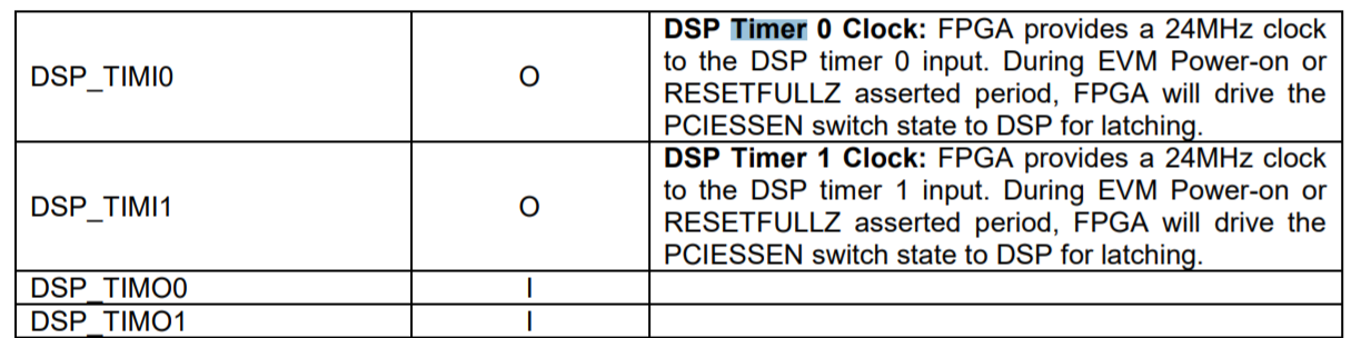
Q1-1 : When we look at the TMS320C6657 EVM, It seems to me that DSP_TIMI[0:1] take input 24Mhz clock from the FPGA. Is it reference clock for DSP Timer?
Q1-2 : What is mandatory input clock to use DSP Internal Timer? Is it possible to use of external OSC instead of FPGA?
Q1-3 : What is the purpose of DSP_TIMO[0:1] in the EVM ?
2. About Reset operation with TMS320C6657 EVM.
Q2-1 : We don't want to use FPGA for RESET#, POR#, RESETFULL# signal. Could you let me know how to control those signal in what signal?
Q2-2 : Could you recommend the best way to control the RESET# signal without using FPGA?
3. About Parallel NOR Flash Boot form EMIF16
Q3-1 : We don't want to use IBL. In this case, as far as we are aware, we should revise built-in ROM boot-loader. Could you let me know what S/W changes must be made in this case?
Q3-2 : There are several chip select (CS0~CS5) for external device. Which one should I use for NOR Flash Boot?
Q3-3 : As far as we are aware, the I2C EEPROM is used to IBL-Booting in TMS320C6657 EVM. What data(information) does EEPROM have?
Q3-4 : If we are designing as IBL booting, do we have to configure Boot Device to I2C Master?
4. About Configuration bootmode with TMS320C6657 EVM
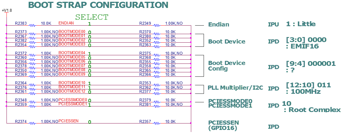
Q4-1 : We have designed our customized board based on TMS320C6657 EVM as can be seen attached schematic. Boot Device configuration pin is BOOTMODE[3:0], right?
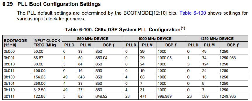
Q4-2 : What does PLL Multiplier signify? Does that mean CORECLK?
5. About Boot Strap Configuration.
Q5-1: When using EMIF16 NAND Flash for booting, how do I set the Boot Strap Configuration for above schematic.
(Coreclk : 50MHz, DDRCLK : 50MHz, PCIE Unused)
Q5-2 : When using EMIF16 NOR Flash(32MB) for booting, how do I set the Boot Strap Configuration for above schematic?
(Coreclk : 50MHz, DDRCLK : 50MHz, PCIE Unused)
Case 1 : If we are using IBL booting...
Case 2 : if we are not using IBL booting...