This thread has been locked.

If you have a related question, please click the "Ask a related question" button in the top right corner. The newly created question will be automatically linked to this question.

CCS/AM5728: PCIe read slow

Part Number: AM5728

Tool/software: Code Composer Studio

1、 Test :

(1)PCIE gen1:SPEED –> 2.5Gb/S、LANE WIDTH -> X2;


 A15@1GHz  -- linux

 DSP@500MHz --TI-RTOS,config PCIE driver,run as RC

 FPGA   run as EP

program use《C:\ti\pdk_am57xx_1_0_4\packages\ti\drv\pcie\example\sample》,not change any driver/bar config

2、 DSP continuity write BAR window:

test like: *(int *)0x21000100=0x1234;

                 *(int *)0x21000104=0x4567;


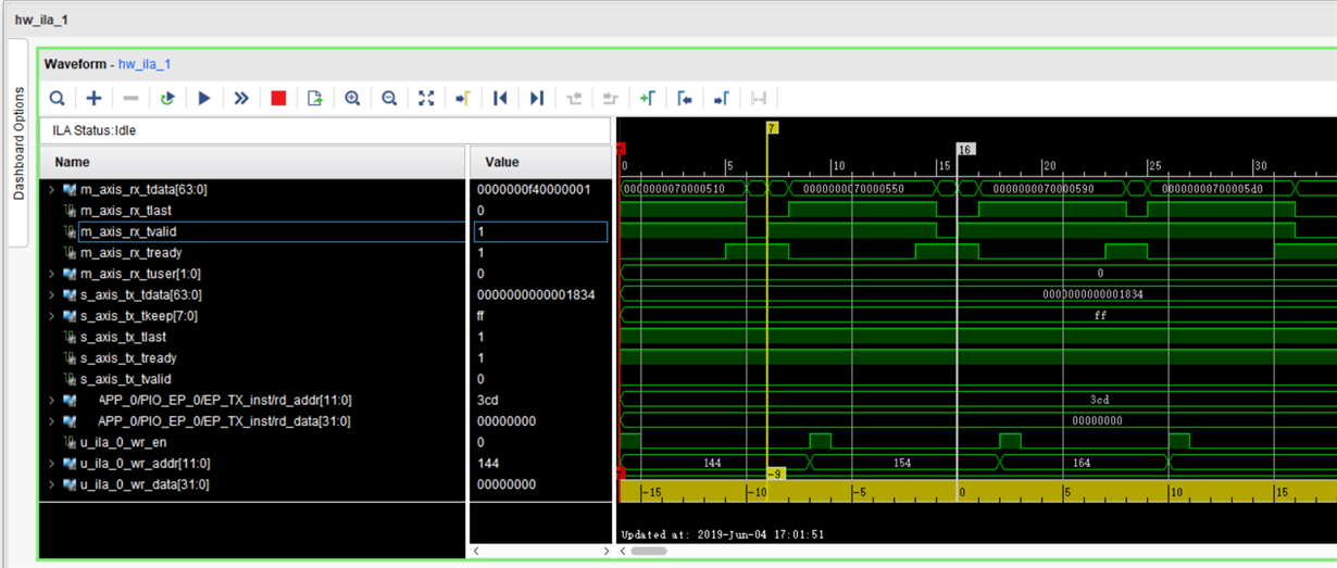
TLP time :

M_axis_rx_xxx are DSP send TLP signal,S_axis_tx_xxx are FPGA reply TLP signal. From above,2 write TLP use 9  CLK time(9*8ns=72ns);

3、DSP continuity read BAR window:

test like : int A=*(int *)0x21000100;

                  int B=*(int *)0x21000104;


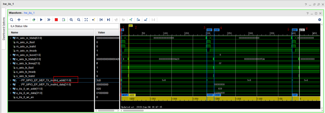
TLP time:

M_axis_rx_xxx are DSP send TLP signal,S_axis_tx_xxx are FPGA reply  TLP signal,Red number 1,3,5 are DSP continuity read 3 times BAR window send TLP timestamp,Red number 2,4,6 are FPGA reply DSP TLP timestamp;

From abve,1st DSP read,FPGA reply in  19-2=17 CLK(17*8=136ns),but between 2 DSP reading TLP the time used(Red number 1,3)202-2=200 clk,that's 1.6us

And I test:  

T1=TSCL;

int A=*(int *)0x21000100;

T2=TSCL;

time used:T2-T1=1.6us  is the same as above.

Thanks

  • Hi,

    The slowness of PCIE read and write using CPU is expected. I recall the throughput is in dozens of MB/s range, far less than the 2.5Gbx2 = 5.0 Gbps = 625 MB/s.

    For high throughput, please use EDMA to move data, the EDMA can generate a read or write burst of 64 bytes. See the RTOS PCIE example http://software-dl.ti.com/processor-sdk-rtos/esd/docs/latest/rtos/index_device_drv.html#pcie. At the end of test, there is EDMA read and write test, the number of cycles used are reported. It is very close to the theoretical value (please also considering 8b/10b encoding, and TLP header (24 or 28 bytes) to each 64 bytes EDMA transfer).

    Regards, Eric 

  • Thanks for your reply.

    Because we use PCIe moving big Datas in DMA mode at FPGA side. So we olny need to check the state of FPGA.Thus we use DSP read 4 or 8bytes state data.How to Improve these readings?  

  • Hi!

    Consider using MSI interrupts to signal FPGA state to processor.

  • Thank you,rrlagic.

    I meam that not only the state of FPGA.

    Maybe some other datas.

    We use some loop buffers share with FPGA. These  need two pointers such as ptrRd and ptrWr.  

    In out way, DSP uses ptrWr to write datas then adjusts ptrWr with the length of datas.And Fpga uses ptrRd to read them then adjusts it.

    DSP or FPGA needs to compare the two pointers determine whether the buffer full or not.

    So DSP needs to read back the two pointers.

  • We also test:long int A=*(long int *)0x21000100; to read 8bytes.

    But it does not work properly.It seems that no TLP transfer to FPGA.

    Why?

  • Hello!

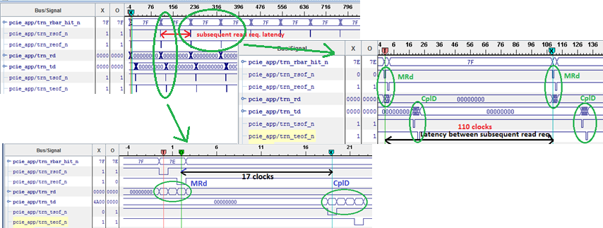
    For your initial question about latency between subsequent MRd's, I found a picture in my records, showing that there is 110 clocks delay (@62.5MHz) between them, although actual completer is sent by FPGA in 17 clocks plus 3 more for TLP itself. This is on C6670. So similar to you we see actual completer is served pretty quickly, but next read request comes with large delay, see figure:

    I have no idea, why it happens, but similar to your case it takes 1.76us between subsequent read requests. My wild guess is that whole serial machinery has about that much latency, and processor cannot issue another PIO read request white current one was not yet serviced.

    Great to know you're happy with DMA of FPGA side. In our case our handmade machine was too far from perfect, so we finally rewrote it to be slave responder, capable to handle multidword TLPs, and run DMA by EDMA3 on DSP side. We lost some performance, but gained multichannel, multiple controller, and quick programming at DSP side.

    Back to your issue, if you are comfortable with FPGA operation, you may try to let FPGA write pointers addresses directly to DSP's dedicated memory locations and signal MSI afterwards, so DSP would look in its own memory and make no read requests to FPGA. On the other hand, FPGA will make posted writes, which should be simple to make and efficient to transfer.

    Hope this helps.

  • Perhaps you tested with long long, ans long int is still 32 bit. If that's a typo, thank you for experiment with (hopefully) 8 byte request. I had a plan to do that myself sometime.

    Again, my guess is that only LDW instruction to PCIe data windows gets translated to MRd TLP with Length=1, but LDDW is not right instruction to that memory range. We better hear people from TI.

  • Hi,

    The PCIE interface is 32-bit, long long to read 64-bit will not work. As rrlagic mentioned, he also observed the lag between subsequent read requests over PCIE link. 

    I thought even you want to read a few 4 or 8 bytes data from FPGA side, you can also use the EDMA of the DSP to try if that reduce the latency. Another way is as he suggested, let FPGA write pointers addresses directly to DSP's dedicated memory locations and signal MSI afterwards, so DSP would look in its own memory and make no read requests to FPGA. On the other hand, FPGA will make posted writes, which should be simple to make and efficient to transfer.

    Regards, Eric

  • Hi.

    I will try your suggestions.Maybe rewrite it in future.

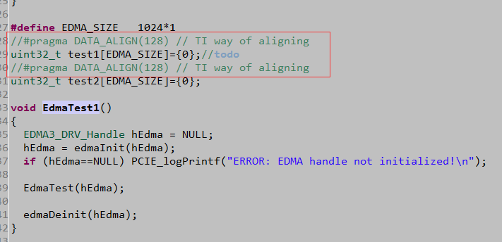
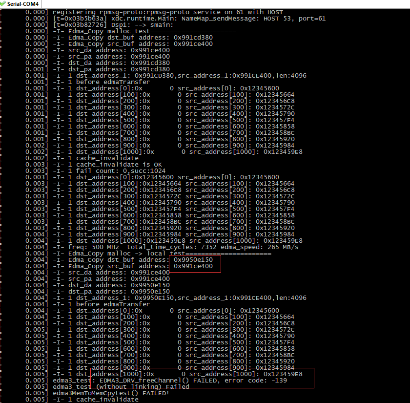
    I had tested eDMA moving datas from RAM to RAM. But it does work property when srcAddr or dstAddr not aligned 128bytes.Is that my using wrong?

  • Hi.

    I had read the example. Setup eDMA is a long path and wait for datas may cost more time.

    Less use of read and FPGA write back directly will be good.

  • Hello!

    If programming EDMA is costly, take a look on its QDMA feature, I recall there is a possibility to trigger pre-configured transfer with just one word write.

    Second, to my knowledge (E/Q)DMA is not strict in alignment, PCIE spec allows non-aligned load through Byte Enable field, but I am not sure whether non-aligned access is permitted by PCIESS of DSP.

  • Hi,

    When using DMA, if the source addressing mode and destination addressing mode is incremental, there is no alignment restriction. If they are constant addressing mode, you must program the address to be aligned to a 256-bit aligned address.

    For the DSP and PCIESS side, non-aligned access is allowed.

    Regards, Eric

  • Hi,

    My partner provides me some test code.

    I try it ,when not aligned address used it can't run.

    EDMATestCode.zip

  • Hi,

    I looked at your source code, you did local DDR to DDR memory copy with aligned/non-aligned address. Probably you will extend this between DDR and PCIE memory space. I knew in many of our drivers, like URAT, MMCSD we used EDMA to move data, and the address is not aligned and still worked. The edma3_test() should set the OPT parameter in source and destination address in incremental mode, so the code looks right.

    I need some time to create a CCS project and test your code, and I will travel next week so expect delay for this. Given you found that unaligned access is not working, are you able to make the source and destination on AM572x EDMA aligned? Or you can move a few or dozens additional data with aligned address, but just discard the un-used. Will you see using EDMA is more efficient to exchange small/un-aligned data with FPGA vs use CPU read reading a few bytes?

    Regards, Eric 

  • Hi,
    I had never used of eDMA. So I asked my partners provided some examples.
    I found that it can not interrupt me when finished.They modified <edma3_lld_2_12_01_25> to solve it.
    I expect to write some functions using eDMA for transfer datas.Such as DDR to DDR, DDR to PCIE memory space, or others.
    Maybe the soucce and destinaltion address alignment mixed 4/8/16/32/64/128 bytes.
    If srcAddr and destAddr must aligned the same sizes, these will limit the use of eDMA.
    My FPGA engineer used the address as register. The test of EDMA  exchange small/un-aligned data doesn't need.
    Have a good travel!
    Time is not critical.
  • Hi,

    If you want to write some EDMA code to move data between DDR and DDR or DDR to PCIE, there are already existing one inside PCIE test example. Please take a look pdk_am57xx_1_0_xx\packages\ti\drv\pcie\example\sample\src\pcie_sample.c. 

    The top level function is PcieExampleEdmaEP() or PcieExampleEdmaRC(). Basically they are the same, and those functions wrapped several layers to the real EDMA API functions for transfer. You can also use your colleague's working EDMA example for this. Moving between DDR or PCIE can be done just replacing the SRC or DST address.  

    The alignment code is:

    #ifdef EDMA
    /* This is the data that will be used as a temporary space holder
    * for the data being transfered using DMA.
    *
    * This is done since EDMA cannot send a specific value or token
    * but instead it can send blocks of data.
    * */
    #ifdef _TMS320C6X
    #pragma DATA_SECTION(dataContainer, ".testData")
    #pragma DATA_ALIGN(dataContainer, PCIE_EXAMPLE_LINE_SIZE)
    #endif
    UInt32 dataContainer[PCIE_EXAMPLE_LINE_SIZE]
    #ifdef __ARM_ARCH_7A__
    __attribute__((aligned(256))) // GCC way of aligning
    #endif
    ; // for dstBuf
    #endif

    Considering possible cache operation, typically we used at least cache line size alignment (you may check if it is 64 or 128 bytes). So using 4/8/16/... for address alignment is not a good choice. 

    Regards, Eric

  • Hi,
    You can see  edma3_test() the same as < pdk_am57xx_1_0_xx\packages\ti\drv\pcie\example\sample\src\pcie_sample.c> in funcion PcieExampleEdmaEP() or PcieExampleEdmaRC().
    From the source code we know that setup eDMA is costly when moving small data.
    When datas in DDR we can make it aligned cache line size. But in peripheral device's spaces,we hard to do.

  • Hello!

    Although LLD is recommended way to deal with EDMA3, I feel it was beneficial to my understanding of this unit to develop my own routines for statically allocated resources. This way I've bound certain activities to their respective controllers and partitioned PaRAM for respective configs. Although we do setup PaRAMs fro every transfer, I see no problem to save pre-configured PaRAM and restore with memcpy() or even explicit word copy once needed. Perhaps QDMA may work for you too.

  • You are right !

    Special routine does special work. 

    Where are the examples for QDMA and other DMA?

  • I found my way looking at pdk_C6678_1_1_2_6\packages\ti\csl\example\edma\edma_test.c. It demonstrates setup of both EDMA and QDMA. And since it's a CSL implementation, the overhead should be smaller comparing to LLD.