


Dear Mr./Mrs,
We are working on a custom board that includes a DRA76P with both QSPI and eMMC flash devices. QSPI P/N is S25FL256ASGMFV001 and eMMC is MTFC8GAMALNA-AAT.
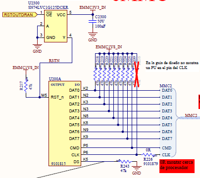
QSPI is working fine. But not the eMMC memory. They are connected like shown:

We are able to flash it with no errors with fastboot.sh (included in the prebuild).
When in u-boot we obtain the next information:
From mmcinfo:
Device: OMAP SD/MMC
Manufacturer ID: 13
OEM: 14e
Name: S0J35
Tran Speed: 200000000
Rd Block Len: 512
MMC version 4.0
High Capacity: Yes
Capacity: 7.3 GiB
Bus Width: 8-bit
Erase Group Size: 512 KiB
While in the EVM MMC version is detected as 4.5...
From ext2ls mmc 1:11
<DIR>       4096 .
<DIR>       4096 ..
<DIR>       4096 benchmarktest
<DIR>       4096 lost+found
<DIR>       4096 nativetest
We are booting Android. If we are not wrong this is the data partition content, before first boot where system, vendor, etc... will be created.
We have configured env to boot from dev 1
mmcboot=if mmc dev ${mmcdev}; then setenv devtype mmc; if mmc rescan; then echo SD/MMC found on device ${mmcdev};if run loadimage; then run loadfdt; echo Booting from mmc${mmcdev} ...; run args_mmc; bootz ${loadaddr} - ${fdtaddr}; fi; fi; fi;
mmcdev=1
But no boot...
This is the dts configuration we are using:
&mmc2 {
	status = "okay";
	vmmc-supply = <&vio_1v8>;
	bus-width = <8>;
	max-frequency = <192000000>;
	ti,non-removable;
	ti,dual-volt;
	cap-mmc-highspeed;
	pinctrl-names = "default", "hs", "ddr_1_8v", "hs200_1_8v";
	pinctrl-0 = <&mmc2_pins_default>;
	pinctrl-1 = <&mmc2_pins_hs>;
	pinctrl-2 = <&mmc2_pins_ddr>;
	pinctrl-3 = <&mmc2_pins_hs200 &mmc2_iodelay_hs200_conf>;
};
	mmc2_pins_default: mmc2_pins_default {
		pinctrl-single,pins = <
			DRA7XX_CORE_IOPAD(0x349c, PIN_INPUT_PULLUP | MUX_MODE1) /* gpmc_a23.mmc2_clk */
			DRA7XX_CORE_IOPAD(0x34b0, PIN_INPUT_PULLUP | MUX_MODE1) /* gpmc_cs1.mmc2_cmd */
			DRA7XX_CORE_IOPAD(0x34a0, PIN_INPUT_PULLUP | MUX_MODE1) /* gpmc_a24.mmc2_dat0 */
			DRA7XX_CORE_IOPAD(0x34a4, PIN_INPUT_PULLUP | MUX_MODE1) /* gpmc_a25.mmc2_dat1 */
			DRA7XX_CORE_IOPAD(0x34a8, PIN_INPUT_PULLUP | MUX_MODE1) /* gpmc_a26.mmc2_dat2 */
			DRA7XX_CORE_IOPAD(0x34ac, PIN_INPUT_PULLUP | MUX_MODE1) /* gpmc_a27.mmc2_dat3 */
			DRA7XX_CORE_IOPAD(0x348c, PIN_INPUT_PULLUP | MUX_MODE1) /* gpmc_a19.mmc2_dat4 */
			DRA7XX_CORE_IOPAD(0x3490, PIN_INPUT_PULLUP | MUX_MODE1) /* gpmc_a20.mmc2_dat5 */
			DRA7XX_CORE_IOPAD(0x3494, PIN_INPUT_PULLUP | MUX_MODE1) /* gpmc_a21.mmc2_dat6 */
			DRA7XX_CORE_IOPAD(0x3498, PIN_INPUT_PULLUP | MUX_MODE1) /* gpmc_a22.mmc2_dat7 */
		>;
	};

	mmc2_pins_hs: mmc2_pins_hs {
		pinctrl-single,pins = <
			DRA7XX_CORE_IOPAD(0x349c, PIN_INPUT_PULLUP | MUX_MODE1) /* gpmc_a23.mmc2_clk */
			DRA7XX_CORE_IOPAD(0x34b0, PIN_INPUT_PULLUP | MUX_MODE1) /* gpmc_cs1.mmc2_cmd */
			DRA7XX_CORE_IOPAD(0x34a0, PIN_INPUT_PULLUP | MUX_MODE1) /* gpmc_a24.mmc2_dat0 */
			DRA7XX_CORE_IOPAD(0x34a4, PIN_INPUT_PULLUP | MUX_MODE1) /* gpmc_a25.mmc2_dat1 */
			DRA7XX_CORE_IOPAD(0x34a8, PIN_INPUT_PULLUP | MUX_MODE1) /* gpmc_a26.mmc2_dat2 */
			DRA7XX_CORE_IOPAD(0x34ac, PIN_INPUT_PULLUP | MUX_MODE1) /* gpmc_a27.mmc2_dat3 */
			DRA7XX_CORE_IOPAD(0x348c, PIN_INPUT_PULLUP | MUX_MODE1) /* gpmc_a19.mmc2_dat4 */
			DRA7XX_CORE_IOPAD(0x3490, PIN_INPUT_PULLUP | MUX_MODE1) /* gpmc_a20.mmc2_dat5 */
			DRA7XX_CORE_IOPAD(0x3494, PIN_INPUT_PULLUP | MUX_MODE1) /* gpmc_a21.mmc2_dat6 */
			DRA7XX_CORE_IOPAD(0x3498, PIN_INPUT_PULLUP | MUX_MODE1) /* gpmc_a22.mmc2_dat7 */
		>;
	};

	mmc2_pins_ddr: mmc2_pins_ddr {
		pinctrl-single,pins = <
			DRA7XX_CORE_IOPAD(0x349c, PIN_INPUT_PULLUP | MUX_MODE1) /* gpmc_a23.mmc2_clk */
			DRA7XX_CORE_IOPAD(0x34b0, PIN_INPUT_PULLUP | MUX_MODE1) /* gpmc_cs1.mmc2_cmd */
			DRA7XX_CORE_IOPAD(0x34a0, PIN_INPUT_PULLUP | MUX_MODE1) /* gpmc_a24.mmc2_dat0 */
			DRA7XX_CORE_IOPAD(0x34a4, PIN_INPUT_PULLUP | MUX_MODE1) /* gpmc_a25.mmc2_dat1 */
			DRA7XX_CORE_IOPAD(0x34a8, PIN_INPUT_PULLUP | MUX_MODE1) /* gpmc_a26.mmc2_dat2 */
			DRA7XX_CORE_IOPAD(0x34ac, PIN_INPUT_PULLUP | MUX_MODE1) /* gpmc_a27.mmc2_dat3 */
			DRA7XX_CORE_IOPAD(0x348c, PIN_INPUT_PULLUP | MUX_MODE1) /* gpmc_a19.mmc2_dat4 */
			DRA7XX_CORE_IOPAD(0x3490, PIN_INPUT_PULLUP | MUX_MODE1) /* gpmc_a20.mmc2_dat5 */
			DRA7XX_CORE_IOPAD(0x3494, PIN_INPUT_PULLUP | MUX_MODE1) /* gpmc_a21.mmc2_dat6 */
			DRA7XX_CORE_IOPAD(0x3498, PIN_INPUT_PULLUP | MUX_MODE1) /* gpmc_a22.mmc2_dat7 */
		>;
	};

	mmc2_pins_hs200: mmc2_pins_hs200 {
		pinctrl-single,pins = <
			DRA7XX_CORE_IOPAD(0x349c, PIN_INPUT_PULLUP | MODE_SELECT | MUX_MODE1) /* gpmc_a23.mmc2_clk */
			DRA7XX_CORE_IOPAD(0x34b0, PIN_INPUT_PULLUP | MODE_SELECT | MUX_MODE1) /* gpmc_cs1.mmc2_cmd */
			DRA7XX_CORE_IOPAD(0x34a0, PIN_INPUT_PULLUP | MODE_SELECT | MUX_MODE1) /* gpmc_a24.mmc2_dat0 */
			DRA7XX_CORE_IOPAD(0x34a4, PIN_INPUT_PULLUP | MODE_SELECT | MUX_MODE1) /* gpmc_a25.mmc2_dat1 */
			DRA7XX_CORE_IOPAD(0x34a8, PIN_INPUT_PULLUP | MODE_SELECT | MUX_MODE1) /* gpmc_a26.mmc2_dat2 */
			DRA7XX_CORE_IOPAD(0x34ac, PIN_INPUT_PULLUP | MODE_SELECT | MUX_MODE1) /* gpmc_a27.mmc2_dat3 */
			DRA7XX_CORE_IOPAD(0x348c, PIN_INPUT_PULLUP | MODE_SELECT | MUX_MODE1) /* gpmc_a19.mmc2_dat4 */
			DRA7XX_CORE_IOPAD(0x3490, PIN_INPUT_PULLUP | MODE_SELECT | MUX_MODE1) /* gpmc_a20.mmc2_dat5 */
			DRA7XX_CORE_IOPAD(0x3494, PIN_INPUT_PULLUP | MODE_SELECT | MUX_MODE1) /* gpmc_a21.mmc2_dat6 */
			DRA7XX_CORE_IOPAD(0x3498, PIN_INPUT_PULLUP | MODE_SELECT | MUX_MODE1) /* gpmc_a22.mmc2_dat7 */
		>;
	};
	/* Corresponds to MMC2_HS200_MANUAL1 in datamanual */
	mmc2_iodelay_hs200_conf: mmc2_iodelay_hs200_conf {
		pinctrl-single,pins = <
			0x190 (A_DELAY(384) | G_DELAY(0))       /* CFG_GPMC_A19_OEN */
			0x194 (A_DELAY(0) | G_DELAY(174))       /* CFG_GPMC_A19_OUT */
			0x1a8 (A_DELAY(410) | G_DELAY(0))       /* CFG_GPMC_A20_OEN */
			0x1ac (A_DELAY(85) | G_DELAY(0))        /* CFG_GPMC_A20_OUT */
			0x1b4 (A_DELAY(468) | G_DELAY(0))       /* CFG_GPMC_A21_OEN */
			0x1b8 (A_DELAY(139) | G_DELAY(0))       /* CFG_GPMC_A21_OUT */
			0x1c0 (A_DELAY(676) | G_DELAY(0))       /* CFG_GPMC_A22_OEN */
			0x1c4 (A_DELAY(69) | G_DELAY(0))        /* CFG_GPMC_A22_OUT */
			0x1d0 (A_DELAY(1062) | G_DELAY(154))	/* CFG_GPMC_A23_OUT */
			0x1d8 (A_DELAY(640) | G_DELAY(0))       /* CFG_GPMC_A24_OEN */
			0x1dc (A_DELAY(0) | G_DELAY(0))         /* CFG_GPMC_A24_OUT */
			0x1e4 (A_DELAY(356) | G_DELAY(0))       /* CFG_GPMC_A25_OEN */
			0x1e8 (A_DELAY(0) | G_DELAY(0))         /* CFG_GPMC_A25_OUT */
			0x1f0 (A_DELAY(579) | G_DELAY(0))       /* CFG_GPMC_A26_OEN */
			0x1f4 (A_DELAY(0) | G_DELAY(0))         /* CFG_GPMC_A26_OUT */
			0x1fc (A_DELAY(435) | G_DELAY(0))       /* CFG_GPMC_A27_OEN */
			0x200 (A_DELAY(36) | G_DELAY(0))        /* CFG_GPMC_A27_OUT */
			0x364 (A_DELAY(759) | G_DELAY(0))       /* CFG_GPMC_CS1_OEN */
			0x368 (A_DELAY(72) | G_DELAY(0))        /* CFG_GPMC_CS1_OUT */
	      >;
	};
Any idea about what is happening?
Thank you very much!

