This thread has been locked.

If you have a related question, please click the "Ask a related question" button in the top right corner. The newly created question will be automatically linked to this question.

TMS320C6747: External Clock (Square Wave) input timing for OSCIN

Part Number: TMS320C6747

Hi,

My customer is using C6747 on their custom board and their current design of power sequence looks like below.

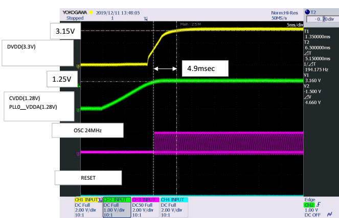
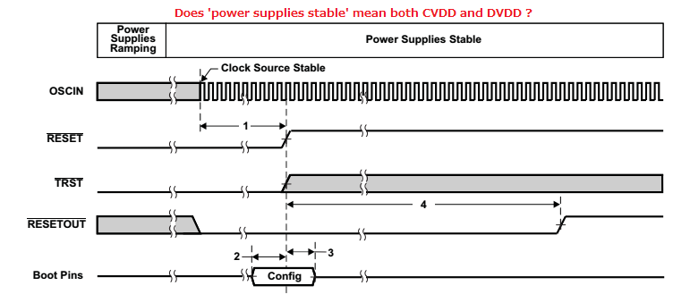
The line in Magenta is external reference clock (Square Wave) input for OSCIN. This clock has been started during the power ramping (especially DVDD). Is this allowed configuration ?

The datasheet actually suggests that the clock should be stable after the power supplies ramping but I'm wondering if CVDD might be sufficient to accept OSCIN input (OSCIN clock should be from 1.2V domain on their custom board).

Best Regards,
NK

  • Hi,

    I got some input from the customer. In the above timing chart, OSCIN is grayed out (don't care) during power supply sequence, so their understanding is the current configuration should be okay. Let me know if you have any concern on this.

    Best Regards,

    NK

  • Hi Naoki,

    The figure you refer to is actually meant to show the timing of the RESET signal (Figure6-4. Power-On Reset (RESET and TRST active) Timing), not the Power supply & CLK ramping up.

    For OSCIN there is actually no requirement specified in the datasheet, neither in Section 6.3 Power Supplies, nor in Section 6.5 Crystal Oscillator or External Clock Input. Let me confirm this with the hw team, but I believe their power-on sequence is okay.

    Best Regards,
    Yordan

  • Hi Naoki-san,

    I agree with Yordan that the OSCIN can start before DVDD is fully ramped. It is on the 1.2V rail, and it is more important for CVDD/ 1.2V to be ramped up before OSCIN begins oscillating. The time from OSCIN running to RESET released is specified in the datasheet.

    Make sure the customer is aware of Errata 2.1.5 System-Level ESD Immunity Usage Note - the rise/fall time of the OSCIN clock needs to be sharp to avoid noise from creating input clock glitches as the OSCIN rise/fall edge crosses the threshold region. A 3.3V oscillator has faster edges and can be used through some level shifter to bring it to the 1.2V range. There are lots of posts on E2E about this concern.

    Regards,
    Mark

  • Hello Mark and Yordan,

    That answers to the customer`s question. I close the thread.

    Best Regards,
    NK