This thread has been locked.

If you have a related question, please click the "Ask a related question" button in the top right corner. The newly created question will be automatically linked to this question.

TDA2P-ACD: Crystal Oscillator amplitude and jitter requirements

Part Number: TDA2P-ACD

Dear TI Members,

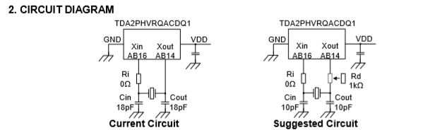
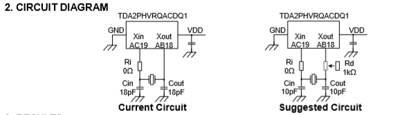
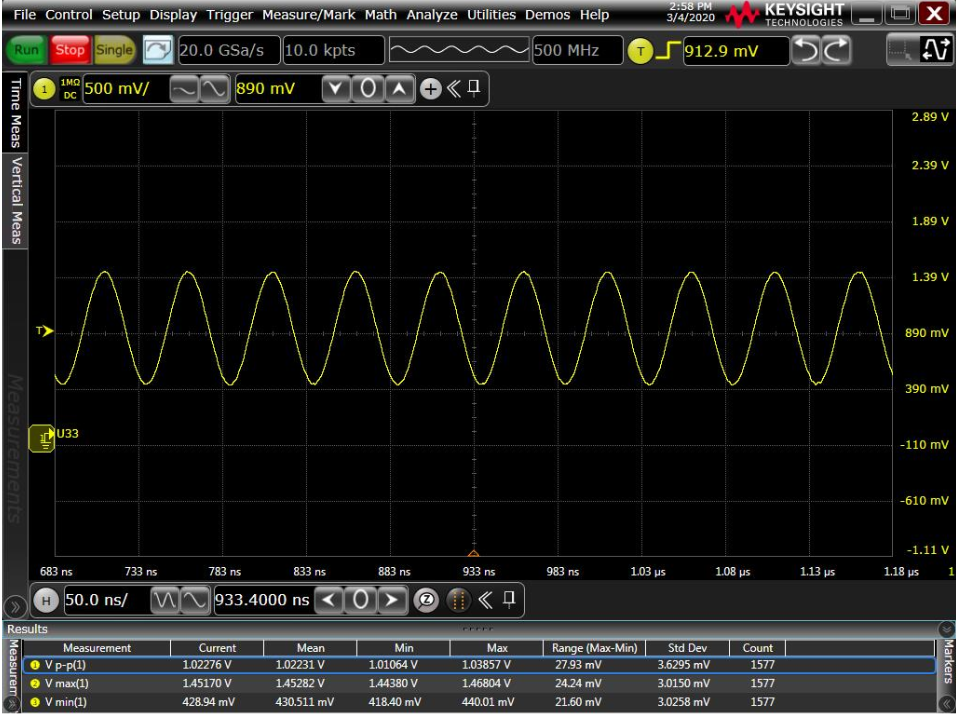
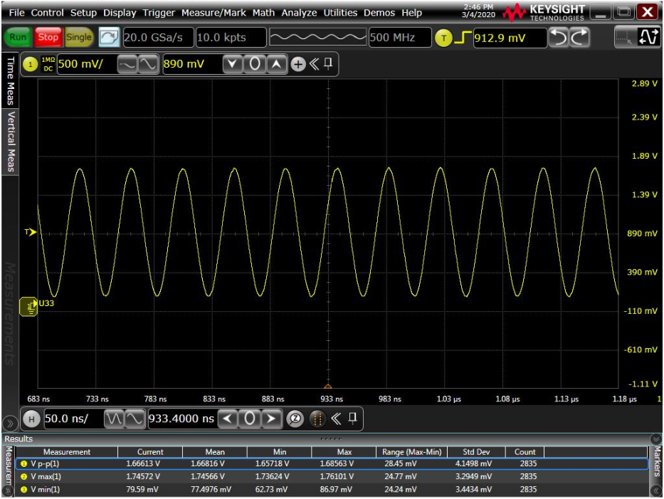
We are trying to validate oscillator design (xi_osc, xo_osc pins)

We have found clear requirements for both jitter and amplitude in the TDA2P-ACD datasheet when an external clock is used.

However, we can not find those requirements when a crystal is used.

Therefore, please, could you make clear which is the expected oscillation amplitude on those pins when a crystal is used?

Additional, please, could you make clear which are the requirements regarding jitter on those pins when a crystal is used?

Thanks so much in advance. Best Regards,

Javi.

  • Dear TI Members,

    Besides, please, we would like to get details information about "gain" of TDA2p internal oscillator stage. For example:

    - Variable gain (Loop control function, gain switch function, …)
    - Constant gain with gain setting (by software)
    - Constant gain without gain setting (ba software)

    Thanks so much in advance. Best Regards,

    Javi

  • Hi Javi,

    I've checked with the datasheet team. They said the current datasheet information should be enough for crystal circuit design. Most of the parameters you are asking are internal to the SoC and cannot be affected.

    Regards,

    Stan

  • Dear Stan,

    As I explained in my first query, we want to validate our design. Information in the datasheet is enough to design but, in my humble opinion, it is not enough to validate our design.

    In my humble opinion, a minimum of information about both jitter and amplitude must be provided to allow your customers to ensure a correct design after checking its functionality according to its corresponding validation process... otherwise, please, how do you advise your clients about validation process for the crystal oscillator circuitry?

    Thanks so much in advance. Best Regards,

    Javi

  • Hi Javi,

    For parameters like oscillator jitter, the whole oscillator design needs to be validated. This includes the oscillator (internal) circuitry, the oscilllator power supply, decoupling, PVT variation. The oscillator has been validated by TI with those taken into account. PCB designers only need to follow SoC datasheet-  and crystal manufacturer-  recommendations for crystal connection to SoC.

    I can recall one possible way to measure the jitter. You can mux (via software or a JTAG) the internal SYS_CLK to one of the clkout pins of the device. Then, measure the jitter on that pin and compare it to the value for external clock-in (not crystal option) in datasheet.

    Regards,

    Stan

  • Dear Stanislav,

    Sorry to jump in, I will be taking over this topic from Javi. Thx for your latest explanation, we will consider your solution for measuring the jitter. 

    Regarding the amplitude specifications which is still not clear:

    In order to adjust the drive level and the negative resistance model of the crystal we would need to know the minimum signal amplitude that your device is able to handle in xi_osc pin.

    We believe that this parameter should be specified in the DS but we are not able to find it. Therefore, would it be possible to clarify which is the expected oscillation amplitude on those pins when a crystal is used?

    Regards,

    Vicent.

    SMR Automotive Mirrors Stuttgart GmbH

  • Let me see if this information is available.  As mentioned previously, following the crystal requirements listed in the datasheet is sufficient to guarantee proper oscillator operation.

  • I was unable to find any specification for the minimum signal amplitude.  Probing the circuit would also introduce additional loading on the oscillator that could distort the waveform.  However, if the datasheet crystal parameters are followed, you should expect to see near rail-to-rail (0V-1.8V) oscillation.

  • Hello B.C,

    Sorry for my late response and thx for your answer.

    With our current design we are around 0V-1.75V. This question arises because our crystal manufacturer is about to perform some tuning of the crystal circuitry and the minimum amplitude value of this signal is an important information for them. 

    They are now starting to perform the test. I will get back to you and check the new value if the signal amplitude is significantly affected after their tuning.

    BR,

    Vicent

  • Thanks for the update, Vincent.

  • Hello B. C.

    Our supplier has already performed the tuning of their crystal on our design and they suggest to place a series resistor (Rd) of value 1K in order to adjust the drive strength of the IC output.

    As expected, when we implement this new Rd, we get a considerable reduction of the signal amplitude in the TDA input pin (New Vpp = ~1V). 

    Is this signal amplitude still enough for the system to work in a comfortable condition? We really miss this specification in the datasheet. 

    You can find osc pics below comparing the signal amplitude in TDA xtal input pin before and after placing the new Rd

    -----------------------------------------------------------------------------------------------------------------------------------------------------------------------------------------------------------------------------

    U33 Original condition

    U33 new condition:


    U34 Original condition:


    U34 new condition:


  • I've confirmed that the VIL/VIH specs for the oscillator input are:

    VIL: 0.35*VDD (max)

    VIH: 0.65*VDD (min)

    In addition to meeting the VIL/VIH requirements, please also make sure that the crystal supplier has done the analysis to confirm that the new damping resistor is not large enough to negatively impact the crystal start-up.

  • Hi B.C.

    Thx for the information. we will consider this values as the crystal input limits for the TDA. 

    According to our crystal manufacturer they have performed the tuning of the crystal circuitry on a wide range of temperatures. 

    Thank you very much for your support.