This thread has been locked.

If you have a related question, please click the "Ask a related question" button in the top right corner. The newly created question will be automatically linked to this question.

TMS320C6657: DDR 3 error

Part Number: TMS320C6657

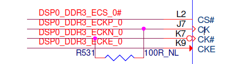
What we drew the DDR circuit of tms320c6657 is shown in the attachment. The MPN of DDR3 is micron mt41k64m16tw-107, and the DDR rate is configured at 800mt / s. At present, the products using this circuit have been shipped in batches. Recently, we returned 3pcs PCBA (two batches). Fault phenomenon: after PCBA is powered on, the DDR self-test sometimes passes, sometimes fails. When DDR test fails, the contents of low bytes read and written in The content is inconsistent and the high byte is read and written correctly. We ruled out the problems of welding, power supply and DSP power on timing. Later, after further testing, we found that after welding 100 Ω resistor at r531 position in the figure below, the phenomenon of DDR self-test failure disappeared. If r531 does not weld 100 Ω resistor, the phenomenon of DDR self-test failure will appear again. We suspect that it may be related to timing, so we are not in R 531 solder 100 Ω resistor, but try to modify the parameter configuration of DDR refresh, Cl, CWL, ODT, etc., and modify the DDR transmission rate, but DDR self-test still fails.

Please help to analyze:

1. Why can welding 100 Ω resistance DDR in r531 get up and get rid of it?

2. If r531 is not welded, can the same effect be achieved by configuring DDR controller parameters? What parameters need to be configured?
  • Hi Elan,

    This could be a timing issue or it could be a signal integrity issue.  Can you reconfigure the DDR interface to operate at a slower speed to see if it operates correctly without the resistor?  Did you check the length matching of all the address/command and data signal trace lengths to be sure it meets the recommendation provided by TI?

    Regards, Bill

  • Hi Bill

            Thanks for your help.

            Slower speed of DDR can not resolve the problem.

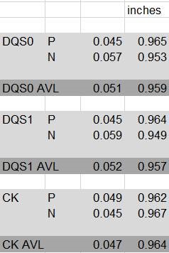
            We have check the DQS & CK PCB trace length,the difference is very small, so we doublt that  the write leveling maybe mismatch, then we reconfig register

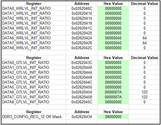
    0x02620414 & 0x02620418 from 0 to 64(Decimal), the issue is resovled.

            For veryfication the write leveling ,we want to konw  TMS320C6657 have the write leveling result register?  How can we access the register?

    Best regards

    Lei

  • We have found the mistake of configuration for WL_INIT and GT_INIT.

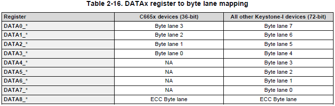
    we use Byte0 and Byte1 of C6657, and should configure the WL_INIT and GT_INIT in the REG DATA3_* and DATA2_*, but we configured in DATA7_* and DATA6_* according "PHY calculation spreadsheet" because of misunderstanding.

    According to the spreadsheet, we re-configured the WL_INIT and GT_INIT, and it seems the board work properly.

    I still have some questions about the training:

    1. We found Byte0 is always wrong and Byte1 is always right when using the error configuration(actually WL_INIT=0 and GT_INIT=0), why exception will not occur in Byte1? 

    Times:1, Start to do ddr test!
    Fail Address:80000004, Write:80000004, Read:80ff002e
    Times:1, DDR test failed!, test result is:-3
    Times:2, Start to do ddr test!
    Fail Address:80000004, Write:80000004, Read:80ff002e
    Times:2, DDR test failed!, test result is:-3
    Times:3, Start to do ddr test!
    Fail Address:80000004, Write:80000004, Read:80ff002e
    Times:3, DDR test failed!, test result is:-3
    Times:4, Start to do ddr test!
    Fail Address:80000004, Write:80000004, Read:80ff002e
    Times:4, DDR test failed!, test result is:-3
    Times:5, Start to do ddr test!
    Fail Address:80000000, Write:80000000, Read:80390010
    Times:5, DDR test failed!, test result is:-3
    Times:6, Start to do ddr test!
    Fail Address:80000000, Write:80000000, Read:80000010
    Times:6, DDR test failed!, test result is:-3
    Times:7, Start to do ddr test!
    Fail Address:80000000, Write:80000000, Read:80000010
    Times:7, DDR test failed!, test result is:-3
    Times:8, Start to do ddr test!
    Fail Address:80000000, Write:80000000, Read:80000010
    Times:8, DDR test failed!, test result is:-3
    Times:9, Start to do ddr test!
    Fail Address:80000000, Write:80000000, Read:80000010
    Times:9, DDR test failed!, test result is:-3

    2. There are 3 types of training( write leveling, read DQS gate training, read date eye training), is there any training result REG? 

     I haven't found timeout flag in WRLVLTO/RDLVGATETO/RDLVLTO, it seems exception during training.

    3. We do some scan about WL_INIT and GT_INIT for 2 boards(as we don't know the training result REG, we use write and read function to verify the results, green is OK and fail in red), and the condition are following:

    The results are following:

    According the test result above, I have some questions:

    a)GT_INIT affect Write Leveling? It's hard to understand.

    b)It seems that the WL_INIT affect DQS Gate training for board1.

    4. I tested the waveform of write leveling, and it seems the WL_INIT of Byte0 doesn't affect Write Leveling result, because we initial position of DQS0 is aligned with the falling edge of CLK when WL_INIT=0, and add additional 1/4T when WL_INIT=0x40, but they synchronize to the same rising edge of CLK. Am I right? If so, the WL_INIT should not affect Write Leveling?

  • Add pictures.

    We have found the mistake of configuration for WL_INIT and GT_INIT.

    we use Byte0 and Byte1 of C6657, and should configure the WL_INIT and GT_INIT in the REG DATA3_* and DATA2_*, but we configured in DATA7_* and DATA6_* according "PHY calculation spreadsheet" because of misunderstanding.

    According to the spreadsheet, we re-configured the WL_INIT and GT_INIT, and it seems the board work properly.

    I still have some questions about the training:

    1. We found Byte0 is always wrong and Byte1 is always right when using the error configuration(actually WL_INIT=0 and GT_INIT=0), why exception will not occur in Byte1?

    Times:1, Start to do ddr test!
    Fail Address:80000004, Write:80000004, Read:80ff002e
    Times:1, DDR test failed!, test result is:-3
    Times:2, Start to do ddr test!
    Fail Address:80000004, Write:80000004, Read:80ff002e
    Times:2, DDR test failed!, test result is:-3
    Times:3, Start to do ddr test!
    Fail Address:80000004, Write:80000004, Read:80ff002e
    Times:3, DDR test failed!, test result is:-3
    Times:4, Start to do ddr test!
    Fail Address:80000004, Write:80000004, Read:80ff002e
    Times:4, DDR test failed!, test result is:-3
    Times:5, Start to do ddr test!
    Fail Address:80000000, Write:80000000, Read:80390010
    Times:5, DDR test failed!, test result is:-3
    Times:6, Start to do ddr test!
    Fail Address:80000000, Write:80000000, Read:80000010
    Times:6, DDR test failed!, test result is:-3
    Times:7, Start to do ddr test!
    Fail Address:80000000, Write:80000000, Read:80000010
    Times:7, DDR test failed!, test result is:-3
    Times:8, Start to do ddr test!
    Fail Address:80000000, Write:80000000, Read:80000010
    Times:8, DDR test failed!, test result is:-3
    Times:9, Start to do ddr test!
    Fail Address:80000000, Write:80000000, Read:80000010
    Times:9, DDR test failed!, test result is:-3

    2. There are 3 types of training( write leveling, read DQS gate training, read date eye training), is there any training result REG?

    I haven't found timeout flag in WRLVLTO/RDLVGATETO/RDLVLTO, it seems exception during training.

    3. We do some scan about WL_INIT and GT_INIT for 2 boards(as we don't know the training result REG, we use write and read function to verify the results, green is OK and fail in red), and the condition are following:

    The results are following:

    According the test result above, I have some questions:

    a)GT_INIT affect Write Leveling? It's hard to understand.

    b)It seems that the WL_INIT affect DQS Gate training for board1.

    4. I tested the waveform of write leveling, and it seems the WL_INIT of Byte0 doesn't affect Write Leveling result, because we initial position of DQS0 is aligned with the falling edge of CLK when WL_INIT=0, and add additional 1/4T when WL_INIT=0x40, but they synchronize to the same rising edge of CLK. Am I right? If so, the WL_INIT should not affect Write Leveling?

  • Hi Elan,

    I am a little confused by your posts.  You stated that you found an error in your initialization and the fixing the error allowed the board to operate correctly.  Are you asking why the incorrect initialization did not work? 

    You also posted some length matching data for the DQSp/n and the clock signals.  The DDR3 implementation guide does not include a routing requirement that these signals be length matched.   The clock needs to be length matched to the address and command signal to both DDR3 devices.  The DQS0p/n needs to be length matched to the lowest data byte lane (DQ0-7) and the DSQ1p/n needs to be length matched to the next byte lane (DQ8-15).  Are you sure you have length matched the DDR traces correctly?

    Regards, Bill

  • Lei,

    Please follow the steps discussed in the appnote linked below.  This will result in a robust solution.  If you need additional support, please post completed PHY_CALC and REG_CALC spreadsheets and a length matching report showing that all of the length matching rules have been met.

    If you are curious why the improper configuration was functional, it is due to the significant timing margin available when operating with nominal silicon.  The timing margins are sufficient to obtain robust operation across variations of voltage, temperature and silicon variation.

    Tom

  • Hi Tom,

           The spreadsheets is attached below, and my questions are listed above.

    DDR3 PHY Calc v10-20191224.xlsx

    I think the issue is that the improper configuration result in the failure of training, so I want to know how to verify the result of training.

  • Lei,

    I need to see the length matching report as well.

    Tom

  • Lei,

    Also note that you are attaching an obsolete PHY_CALC sheet.  The version linked through the appnotes is v11.  Please provide a properly completed v11 worksheet.

    Tom

  • Tom

            Please provide the link of V11 PHY_CALC sheet, thanks.

  • Lei

    It is part of the following application note zip folder

    http://www.ti.com/lit/an/sprabl2e/sprabl2e.pdf

    Regards

    Mukul

  • Hi Tom

    The DDR3 PHY Calc v11 attachment listed below: 

            7750.DDR3 PHY Calc v11.xlsx

  • Lei,

    I provided the link for the summary appnote.  It links to other appnotes, including the one that supports the PHY_CALC worksheet.  You have asked about the methodology to know that the implementation is robust.  You need to familiarize yourself with these documents so that you can properly commission your DDR interface.

    As part of the commissioning process you need to prepare and provide a report showing that the length matching rules have been met.  The results from this report are then used to populate the PHY_CALC worksheet.

    Tom

  • Tom

    Thanks for your help very much.

    Can you reply Lan questions?  How can we know the leveling & traing result is OK after DDR initialization? Is there leveling & traing status register?

  • Lei,

    You are missing what I keep saying.  If you want to have a robust DDR3 interface, you must complete all of the steps to commission the interface.  Robust DDR3 operation requires careful implementation in both the hardware and software.  DDR3 write leveling is a process that aligns a clock edge with a DQS edge at the SDRAM.  DDR3 read leveling then estimates the round-trip delay from clock launch to DQS being received back to the PHY.  In this device, leveling is a hardware state machine driven process.  There are the 3 TO bits in the status register but they only indicate that the hardware state machines completed.  They have no knowledge of data integrity.  If you want a data integrity test, you would need to add it to your boot code after leveling has completed.  However, that is not needed.  If you have a properly designed board and you follow all of the commissioning steps discussed in the appnotes, you can have confidence that the DDR3 interface will operate robustly.

    I have still not seen evidence that you have completed the commissioning steps.  Please provide this.

    Tom