


Part Number: AM3352
Hello,
We have some questions for the structure of the IO termination on AM3352.
We are focusing on A17(SPI0_SCLK), B17(SPI0_D0), B16(SPI0_D1) and A16(SPI0_CS0) on AM3352BZCZ.
1.Could you share the figure showing the structure of the IO termination of A17(SPI0_SCLK), B17(SPI0_D0), B16(SPI0_D1) and A16(SPI0_CS0) on AM3352BZCZ?
2.In case the above terminations are set to SPI and in case of SPI read, could you tell me the point where the clock signal of SPI is looped back?
Also, is this point effected by the reflection from the output termination?
The followings are background.
- AM3352 sends a read command to the SPI Flash memory which is connected to A17, B17, B16 and A16.
- Sometimes, the read data is different from the expected data.
- The SPI clock frequency is 48MHz, and the mode is in burst read.
- We've already checked the waveform and the waveform seems to be good (We've used the feature in an oscilloscope)
- However, the data in AM3352 is not the expected data. (For example, the expected data is 0x2E, but the data in AM3352 is 0x5E)
- The frequency of this phenomenon is only 1 time per about 3MB.
- This phenomenon appears only in the case of that the dumping resistance is 0 ohm which is marked by a red rectangle in the following figure.
- However, in case the resistance changes to 22 ohms, this phenomenon seems to be not happened.
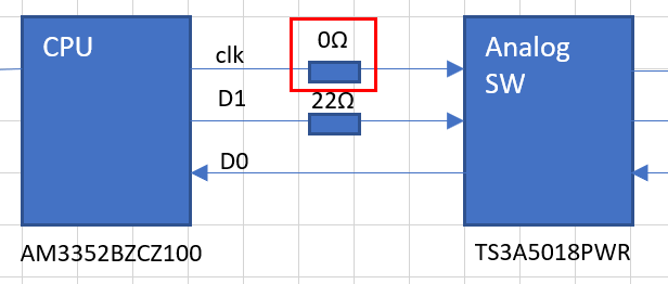
We want to know your view for this result.
Best Regards,
Nomo

