This thread has been locked.

If you have a related question, please click the "Ask a related question" button in the top right corner. The newly created question will be automatically linked to this question.

PROCESSOR-SDK-AM335X: Timer pinmuxing

Part Number: PROCESSOR-SDK-AM335X
Other Parts Discussed in Thread: CCSTUDIO

Hi,

I am using SKAM335x board and TI RTOS SDK on windows host PC.

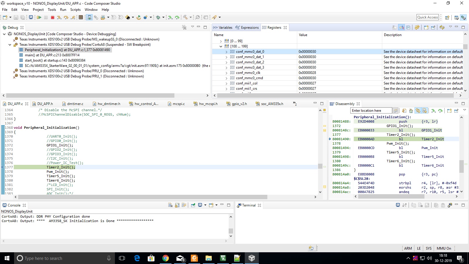
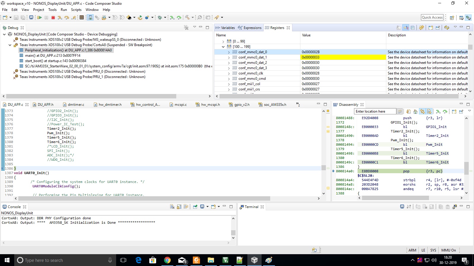
I am doing pinmuxing for F18 (Timer6) and F17 (Timer 5) by control module registers Conf_MMC_DATA2 and Conf_MMC_DATA3 respectively. I am using offset address 0x8f4 and 0x8f0 for these registers but it is writing in Conf_MMC_DATA1 and Conf_MMC_DATA0 respectively. I think offset address are interchanged. Can you check and confirm?

Regards

Gaurav

  • Hi Gaurav,

    From what I can find, pin F18 (mmc0_dat2) is at offset 0x8F4, which match with AM335x TRM Table 9-10. CONTROL_MODULE REGISTERS. I can see that this is the offset value used in AM335x TI PSDK Linux Full address of register conf_mmc0_dat2 is 0x44E108F4. You can explore below files for reference:

    u-boot-2019.01/arch/arm/dts/am335x-icev2.dts

    u-boot-2019.01/arch/arm/include/asm/arch-am33xx/mux_am33xx.h

    linux-4.19.59/arch/arm/boot/dts/am335x-evm.dts

    linux-4.19.59/arch/arm/boot/dts/am335x-icev2-common.dtsi

    mmc0_pins_default: mmc0_pins_default {
            pinctrl-single,pins = <
                AM33XX_IOPAD(0x8f0, PIN_INPUT_PULLUP | MUX_MODE0) /* (F17) mmc0_dat3.mmc0_dat3 */
                AM33XX_IOPAD(0x8f4, PIN_INPUT_PULLUP | MUX_MODE0) /* (F18) mmc0_dat2.mmc0_dat2 */
                AM33XX_IOPAD(0x8f8, PIN_INPUT_PULLUP | MUX_MODE0) /* (G15) mmc0_dat1.mmc0_dat1 */
                AM33XX_IOPAD(0x8fc, PIN_INPUT_PULLUP | MUX_MODE0) /* (G16) mmc0_dat0.mmc0_dat0 */
                AM33XX_IOPAD(0x900, PIN_INPUT_PULLUP | MUX_MODE0) /* (G17) mmc0_clk.mmc0_clk */
                AM33XX_IOPAD(0x904, PIN_INPUT_PULLUP | MUX_MODE0) /* (G18) mmc0_cmd.mmc0_cmd */
            >;
        };


    Regards,
    Pavel

  • Gaurav,

    AM335x PDK source code also match with AM335x TRM Table 9-10. CONTROL_MODULE REGISTERS. This means pin F18 mmc0_dat2 is at offset 0x8F4. You can explore below files for reference:

    pdk_am335x_1_0_16/packages/ti/starterware/board/am335x/am335x_gpevm_pinmux_data.c

    pdk_am335x_1_0_16/packages/ti/starterware/board/am335x/am335x_pinmux.h

    pdk_am335x_1_0_16/packages/ti/starterware/include/hw/hw_control_am335x.h


    Regards,
    Pavel

  • Hi Pavel

    I am also using 0x8f4 offset address to write in mmc0_dat2 register but I checked in debug mode, it is writing in mmc0_dat1 register. Can you check at your end?

    Regards

    Gaurav

  • Gaurav,

    Can you provide me your exact steps to reproduce this issue on my side?

    Meanwhile make sure you are using full address of 0x44E108F4.


    Regards,
    Pavel

  • Pavel,

    #define SOC_CONTROL_REGS                     (0x44E10000)

    #define SOC_DMTIMER_6_REGS                   (0x48048000)

    void Timer6_Init(void)
    {
    /* This function will enable clocks for the DMTimer6 instance */
    DMTimer6ModuleClkConfig();

    /* This function perform pinmuxing for the DMTimer6 instance */
    Timer_Pinmux(CONTROL_CONF_MMC0_DAT2, (CONTROL_CONF_RXACTIVE|CONTROL_CONF_MUXMODE(3)|CONTROL_CONF_PULLUPSEL));

    /* Perform the necessary configurations for DMTimer6 */
    DMTimer_PWMSetUp(SOC_DMTIMER_6_REGS);

    /* Start the DMTimer */
    DMTimerEnable(SOC_DMTIMER_6_REGS);
    }

    void Timer_Pinmux(uint32_t ConfReg, uint32_t PinMuxValue)
    {

    HWREG(SOC_CONTROL_REGS + ConfReg) = PinMuxValue;

    }

    static void DMTimer_PWMSetUp(uint32_t baseadd)
    {
    /* Load the counter with the initial count value */
    DMTimerCounterSet(baseadd, TIMER5_PWM_INITIAL_COUNT);

    /* Load the load register with the reload count value */
    DMTimerReloadSet(baseadd, TIMER5_PWM_RLD_COUNT);

    /* Configure the DMTimer for Auto-reload and compare mode */
    DMTimerModeConfigure(baseadd, DMTIMER_AUTORLD_NOCMP_ENABLE|DMTIMER_TCLR_SCPWM|DMTIMER_TCLR_TRG_OVERFLOWANDMATCH|DMTIMER_TCLR_CE|DMTIMER_TCLR_PT);

    }

    Regards

    Gaurav

  • Gaurav,

    Gaurav Aggarwal1 said:
    #define SOC_CONTROL_REGS                     (0x44E10000)

    Gaurav Aggarwal1 said:
    /* This function perform pinmuxing for the DMTimer6 instance */
    Timer_Pinmux(CONTROL_CONF_MMC0_DAT2, (CONTROL_CONF_RXACTIVE|CONTROL_CONF_MUXMODE(3)|CONTROL_CONF_PULLUPSEL));

    Gaurav Aggarwal1 said:

    void Timer_Pinmux(uint32_t ConfReg, uint32_t PinMuxValue)
    {

    HWREG(SOC_CONTROL_REGS + ConfReg) = PinMuxValue;

    }

    Based on the above code, how exactly you define that you are writing into conf_mmc0_dat1/0x8F8 instead of conf_mmc0_dat2/0x8F4 ? What makes you think you are writing to conf_mmc0_dat1/0x8F8 with the above code?

    Regards,
    Pavel

  • Pavel,

    I checked in debug mode in registers section.

    Regards

    Gaurav

  • Gaurav,

    Gaurav Aggarwal1 said:
    I checked in debug mode in registers section.

    Can you provide me a screen shot (print screen) of the registers you are observing?

    Regards,
    Pavel

  • Pavel,

    Please find screenshot.

  • Gaurav,

    Seems that we have error in CCStudio xml file:

    ccs910/ccs/ccs_base/common/targetdb/Modules/am335x/control_module.xml

    <register acronym="conf_mmc0_dat_2" description="See the device datasheet for information on default pin mux configurations. Note that the device ROM may change the default pin mux for certain pins based on the SYSBOOT mode settings." id="conf_mmc0_dat_2" offset="0x8F8" width="32">

    The correct offset for conf_mmc0_dat_2 should be 0x8F4. Check below e2e thread which discuss the same issue:

    https://e2e.ti.com/support/processors/f/791/t/762998


    I will notify the CCS team for this error to be fixed.

    Regards,
    Pavel

  • Pavel,

    I will consider address given in TRM.

    Thanks & Regards

    Gaurav