This thread has been locked.

If you have a related question, please click the "Ask a related question" button in the top right corner. The newly created question will be automatically linked to this question.

AM5748: GPMC pinmux issue

Part Number: AM5748

Hi

In our custom AM5748 design we use the GPMC interface to connect a SRAM and MRAM to the Sitara. The SRAM uses CS0 and MRAM CS1. The interface consists of 8 data bits, 20 address bits, WEN and OEN_REN.

  • SRAM is located at 0x0100'0000
  • MRAM is located at 0x0200'0000

In PinMux tool we configured the interface as "non-multiplexed 8b NOR type - asynchronous" with default timing. 

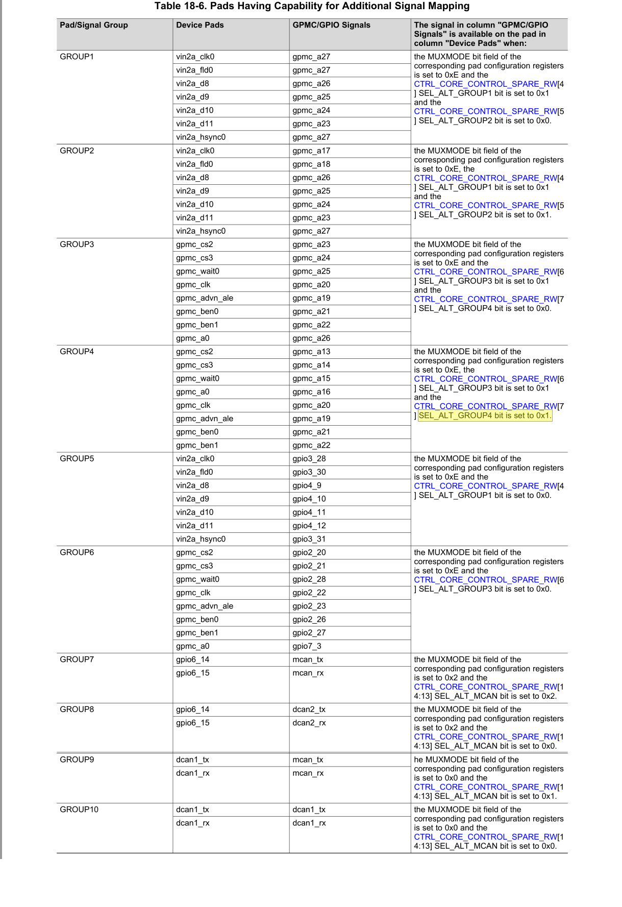
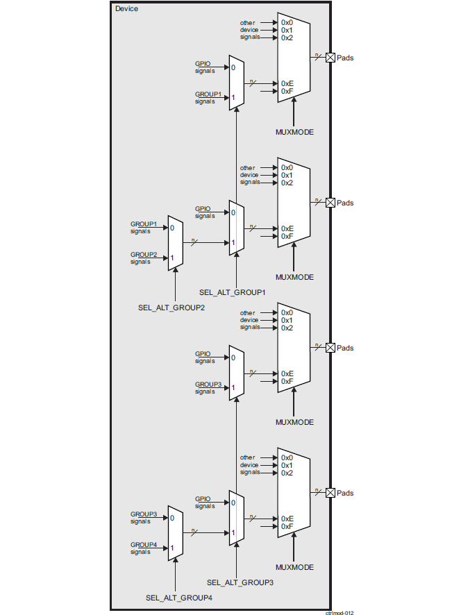
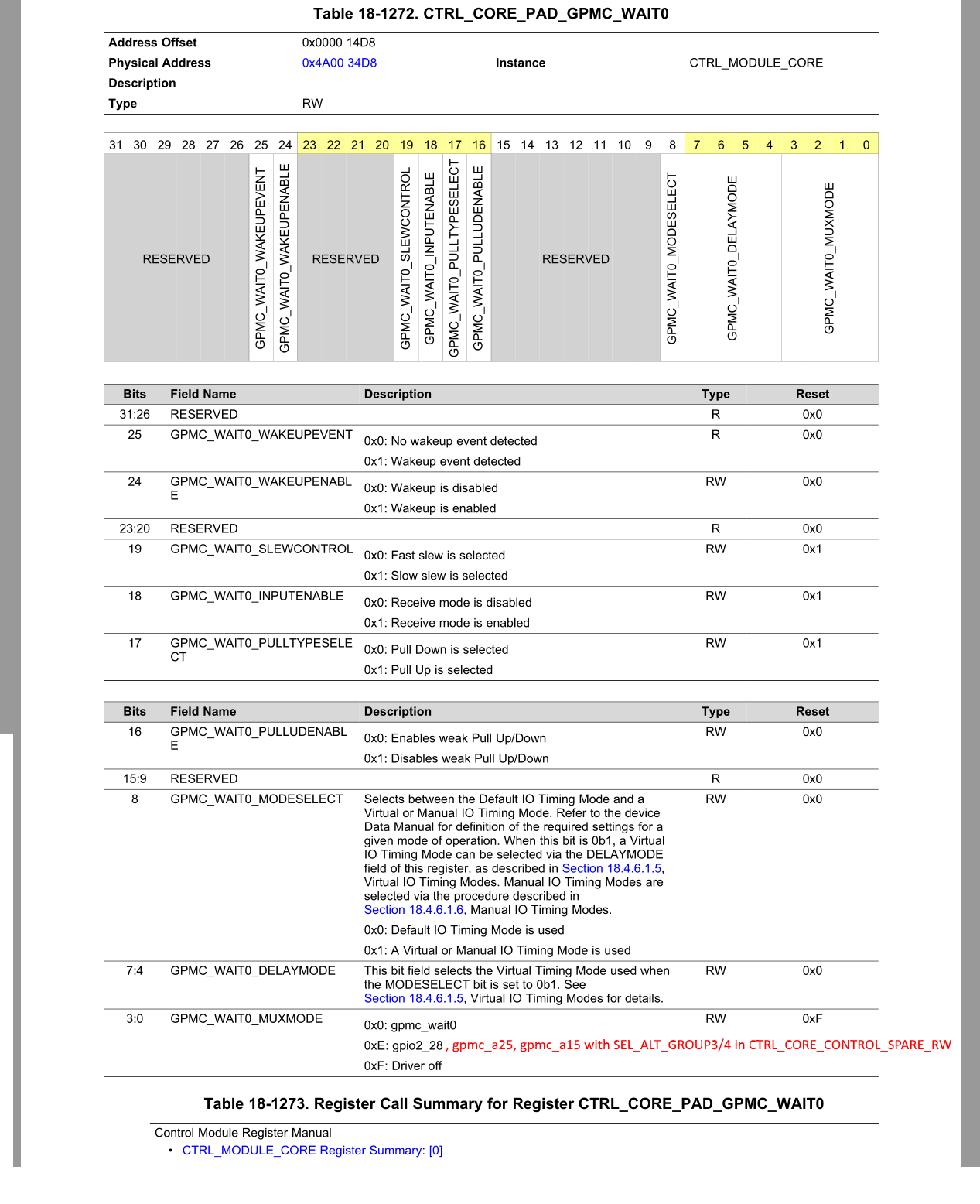
The problem we experience is that the first 32kB are mirrored throughout the wole address range (2Mbyte). The behaviour is the same for SRAM and MRAM. The device tree under Linux looks ok. We were able to see that address signal A15 of the GPMC interface is never high, the voltage is stuck at around 650mV. I checked the PinMux output file "genericFileFormatPadConf.txt and there I noticed that the MuxMode hasn't been set correctly.3

Screenshot "genericFileFormatPadConf.txt"

In the output file ball N2 is set to MuxMode 14, which according to the datasheet is correct. However MuxMode 14 is also for pgio2_28 and gpmc_a25.

According to the TRM the corresponding register only supports:

  • gpmc_wait0
  • gpio2_28
  • Driver off

Screenshot datasheet

Screenshot TRM

Screenshot PinMux tool

it seems that ball N2 is configured as gpio2_28 and input functionality. How can I configure N2 to have the functionality of GPMC_A15? Why does MuxMode 14 contain 3 different signal names (functions)?

Thanks for your help.

Best regards,

Roger

  • Hi Roger,

    There is a secondary pin mux for a handful of pins including GPMC_WAIT0. It can be muxed with GPMC_A15 as part of GROUP4. Select GROUP4 by setting SEL_ALT_GROUP3 = 0x1 and SEL_ALT_GROUP4 = 0x1 in register CTRL_CORE_CONTROL_SPARE_RW (0x4A00 2E68). Note this may affect any other pins using secondary mux mode.

    Select MUXMODE = 14 (0xE) in the primary mux mode register (CTRL_CORE_PAD_GPMC_WAIT0) to select gpio2_20 or gpmc_a23 or gpmc_a13 through the secondary pin mux.

    In the TRM, refer to...
    * Figure 18-5. Multiplexing Scheme of the Pads Having Capability for Additional Signal Mapping
    * Table 18-6. Pads Having Capability for Additional Signal Mapping

    To bring GPMC_A15 out on pin gpmc_wait0... verify that your pinmux tool is setting up correctly...
    SEL_ALT_GROUP3 bit is set to 0x1
    SEL_ALT_GROUP4 bit is set to 0x1

    Watch out for subsequent code from the PinMuxTool overwriting these bitfields... Check their contents during runtime to be certain. There was a bug fixed in 2017 around this issue.

    Make sure that no siganls are being brought from other groups. Each group controls multiple siganls together. The pinmux tool should catch any of these incompatibile group combinations and warn you.

    The TRM should be clariied so that Table 18-1272 should include GPMC_A15 and mention the secondry mux mode. I will file a ticket on this issue.

    Hope this helps,
    Mark

  • I filed a LitBug against the TRMs of the AM57x family of products to include the secondary mux mode signals with Table 18, where it was missing.

    I went ahead and included all of the pads that support secondary pin muxing. See below.....

    This bug applies to members of the AM57x family (AM572, AM571, AM574, AM576, and automotive equivalents)

    It was a problem for this customer: https://e2e.ti.com/support/processors/f/791/p/870197/3219244#3219244

    TRM Table 18 does not include all possible secondary mux modes for mux mode 14 for the select signals that support secondary pin muxing as listed in Table 18-6. Pads Having Capability for Additional Signal Mapping.

    I have gone through each pad in Table 18-6 and suggested the updates for bits 3:0 MUXMODE...


    Table 18-1334. CTRL_CORE_PAD_VIN2A_CLK0
    0xE: gpio3_28 --> 0xE: gpio3_28, gpmc_a27, gpmc_a17 (Refer to Table 18-6. Pads Having Capability for Additional Signal Mapping)

    Table 18-1338. CTRL_CORE_PAD_VIN2A_FLD0
    0xE: gpio3_30 --> 0xE: gpio3_30, gpmc_a27, gpmc_a18 (Refer to Table 18-6. Pads Having Capability for Additional Signal Mapping)

    Table 18-1360. CTRL_CORE_PAD_VIN2A_D8
    0xE: gpio4_9 --> 0xE: gpio4_9, gpmc_a26 (Refer to Table 18-6. Pads Having Capability for Additional Signal Mapping)

    Table 18-1362. CTRL_CORE_PAD_VIN2A_D9
    0xE: gpio4_10 --> 0xE: gpio4_10, gpmc_a25 (Refer to Table 18-6. Pads Having Capability for Additional Signal Mapping)

    Table 18-1364. CTRL_CORE_PAD_VIN2A_D10
    0xE: gpio4_11 --> 0xE: gpio4_11, gpmc_a24 (Refer to Table 18-6. Pads Having Capability for Additional Signal Mapping)

    Table 18-1366. CTRL_CORE_PAD_VIN2A_D11
    0xE: gpio4_12 --> 0xE: gpio4_12, gpmc_a23(Refer to Table 18-6. Pads Having Capability for Additional Signal Mapping)

    Table 18-1340. CTRL_CORE_PAD_VIN2A_HSYNC0
    0xE: gpio3_31 --> 0xE: gpio3_31, gpmc_a27 (Refer to Table 18-6. Pads Having Capability for Additional Signal Mapping)

    Table 18-1256. CTRL_CORE_PAD_GPMC_CS2
    0xE: gpio2_20 --> 0xE: gpio2_20, gpmc_a23, gpmc_a13 (Refer to Table 18-6. Pads Having Capability for Additional Signal Mapping)

    Table 18-1258. CTRL_CORE_PAD_GPMC_CS3
    0xE: gpio2_21 --> 0xE: gpio2_21, gpmc_a24, gpmc_a14 (Refer to Table 18-6. Pads Having Capability for Additional Signal Mapping)

    Table 18-1272. CTRL_CORE_PAD_GPMC_WAIT0
    0xE: gpio2_28 --> 0xE: gpio2_28, gpmc_a25, gpmc_a15 (Refer to Table 18-6. Pads Having Capability for Additional Signal Mapping)

    Table 18-1260. CTRL_CORE_PAD_GPMC_CLK
    0xE: gpio2_22 --> 0xE: gpio2_22, gpmc_a20 (Refer to Table 18-6. Pads Having Capability for Additional Signal Mapping)

    Table 18-1262. CTRL_CORE_PAD_GPMC_ADVN_ALE
    0xE: gpio2_23 --> 0xE: gpio2_23, gpmc_a19 (Refer to Table 18-6. Pads Having Capability for Additional Signal Mapping)

    Table 18-1268. CTRL_CORE_PAD_GPMC_BEN0
    0xE: gpio2_26 --> 0xE: gpio2_26, gpmc_a21 (Refer to Table 18-6. Pads Having Capability for Additional Signal Mapping)

    Table 18-1270. CTRL_CORE_PAD_GPMC_BEN1
    0xE: gpio2_27 --> 0xE: gpio2_27, gpmc_a22 (Refer to Table 18-6. Pads Having Capability for Additional Signal Mapping)

    Table 18-1196. CTRL_CORE_PAD_GPMC_A0
    0xE: gpio7_3 --> 0xE: gpio7_3, gpmc_a26, gpmc_a16 (Refer to Table 18-6. Pads Having Capability for Additional Signal Mapping)

    Table 18-1488. CTRL_CORE_PAD_GPIO6_14
    0xE: gpio6_14 --> 0xE: gpio6_14

    !!! The following registers have additional problems (original muxmode 14 looks wrong in DM and TRM - confirm with DM owner)
    TRM: Table 18-1488. CTRL_CORE_PAD_GPIO6_14
    0xE: gpio6_14 --> 0xE: gpio6_14, mcan_tx, dcan2_tx (Refer to Table 18-6. Pads Having Capability for Additional Signal Mapping)
    DM: Table 4-1. Pin Attributes
    BALL NUMBER E21 MUXMODE 14 gpio6_14 --> gpio6_14, mcan_tx, dcan2_tx

    TRM: Table 18-1490. CTRL_CORE_PAD_GPIO6_15
    0xE: gpio6_15 --> 0xE: gpio6_15, mcan_rx, dcan2_rx (Refer to Table 18-6. Pads Having Capability for Additional Signal Mapping)
    DM: Table 4-1. Pin Attributes
    BALL NUMBER F20 MUXMODE 14 gpio6_15 --> gpio6_15, mcan_rx, dcan2_rx

    TRM: Table 18-1652. CTRL_CORE_PAD_DCAN1_TX
    0xE: gpio1_14 --> 0xE: gpio1_14, mcan_tx, dcan1_tx (Refer to Table 18-6. Pads Having Capability for Additional Signal Mapping)
    DM: Table 4-1. Pin Attributes
    BALL NUMBER G20 MUXMODE 14 gpio1_14 --> gpio1_14, mcan_tx, dcan1_tx

    TRM: Table 18-1654. CTRL_CORE_PAD_DCAN1_RX
    0xE: gpio1_15 --> 0xE: gpio1_15, mcan_rx, dcan1_rx (Refer to Table 18-6. Pads Having Capability for Additional Signal Mapping)

    DM: Table 4-1. Pin Attributes
    BALL NUMBER G19 MUXMODE 14 gpio1_15 --> gpio1_15, mcan_rx, dcan1_rx

    Regards,
    Mark

  • Hi Mark

    Thanks for your answer.

    Does this mean that I use GROUP4 as additional signal mapping gpmc_wait0 will become gpmc_a15 but also for example gpmc_advn_ale becomes gpmc_a19, even though I have configure that pad in PinMux as GPIO gpio2_23 (MuxMode 16)?

    Why doesn't PinMux support the addional signal mapping?

    Thanks and best regards,

    Roger

  • Roger,

    You are correct.

    I just tried the Cloud-based PinMux tool Version: 4.0.1538 for AM5748. Choosing only gpmc_a15 on N2 (gpmc_wait0, GROUP4) and gpio2_23 on N1 (gpmc_advn_ale, GROUP 6)... It looks like the PinMux tool is not catching this conflict with the secondary pinmux chosen by the SEL_ALT_GROUPn bits.

    /cfs-file/__key/communityserver-discussions-components-files/791/AM5748_5F00_SR1.0.pinmux

    In boardPadDelayInit.c PinMux output file...
    0x4A002E68 is the  CTRL_CORE_CONTROL_SPARE_RW register that includes bits SEL_ALT_GROUP4 (bit 7) and SEL_ALT_GROUP3 (bit 6).

    You can see that the reg is written once for gpio2_23 in GROUP6 (SEL_ALT_GROUP3 = 0), but then it is written again for gpmc_a15 in GROUP4. The result will be that GROUP4 is used, and gpio2_23 will not come out of N1/gpmc_advn_ale. Instead gpmc_a19 will come out of the N1/gpmc_advn_ale pad.

    /* GPIO2 - gpio2_23 on N1 - MyGPIO1 */
         {0x4A002E68, 0x0},
    /* GPMC - gpmc_a15 on N2 - MyGPMC1 */
    #ifdef GPMC_DEFAULT
         {0x4A002E68, 0xC0},
    #endif        
    #ifdef GPMC_VIRTUAL1
         {0x4A002E68, 0xC0},
    #endif        

    I don't know why the tool did not catch this conflict. I will file a bug against the PinMuxTool for this issue.

    I apologize that it lead you down this path. Can you perhaps find another GPIO to use with a board mod?

    Regards,
    Mark

  • Hi Mark

    Thanks for the clarifications.

    According to the TRM, table 18-6, MUXMODE of each signal pad should be set to 0x0E and via CTRL_CORE_CONTROL_SPARE_RW the signal GROUP can be set.

    According to your previous reply, I need to enable GROUP4 in order to get gpmc_a15 onto gpmc_wait0 pad (N2). If I check all signals in GROUP4, not all of them are used in MUXMODE 14. 

    Pad name Ball Signal name according to GROUP4  MuxMode Usage in design
    gpmc_ben1 M4 gpmc_a22 14 gpio2_27
    gpmc_advn_ale N1 gpmc_a19 14 gpio2_23
    gpmc_wait0 N2 gpmc_a15 14 gpmc_a15
    gpmc_ben0 N6 gpmc_a21 14 gpio2_26
    gpmc_cs3 P1 gpmc_a14 5 gpmc_a1
    gpmc_cs2 P2 gpmc_a13 1 qspi_cs0
    gpmc_clk P7 gpmc_a20 14 gpmc_a20
    gpmc_a0 R6 gpmc_a16 0 gpmc_a0

    So if I set SEL_ALT_GROUP3 to 0x01 and SEL_ALT_GROUP4 to 0x01, will the signals which aren't in MUXMODE 14 also be affected? Meaning that for example gpmc_a14 will become gpmc_a1? These are the critical signals because I could change the GPIOs but changing the other signals could be tricky, especially qspi_cs0.

    Regards,

    Roger

  • Hi Roger,

    The secondary pin muxing is only selected when the primary muxmode is 0xE (14d) as selected by the MUXMODE bits of the CTRL_CORE_PAD_n registers.

    Roger Newbould31 said:
    So if I set SEL_ALT_GROUP3 to 0x01 and SEL_ALT_GROUP4 to 0x01, will the signals which aren't in MUXMODE 14 also be affected?

    No, since the signal is not in MUXMODE 14 it is not affected by the SEL_ALT_GROUP3 to 0x01 and SEL_ALT_GROUP4. An example of this is your gpmc_cs3 in MUXMODE 5 selecting gpmc_a1. This will continue to be gpmc_a1 regardless of the SEL_ALT_GROUPn bits.

    You can see this in the picture of the muxes feeding into the MUXMODE 14 pin in the below figure.

    It sounds like you are understanding this secondary pinmuxing correctly. Let me know if I can further clarify anything.

    The TRM will be updated in the near term accordingly.

    Regards,
    Mark

  • Hi Mark

    Thanks again for your support. 

    By enabling GROUP4 I have to resolve another conflict. gpmc_advn_ale (N1) will become gpmc_a19, which in my current design is mapped to J6. I will need to re-assign the signal in the schematic and also in PinMux. However this will free up gpio2_15 (J6, MuxMode 0x0E) which I can use for other purposes.

    Will the PinMux tool be able to support the additional signal mapping capabilites and also highlight conflicts?

    Regards,

    Roger

  • Hi Mark

    Thanks again for your support.

    By enabling GROUP4 I have to resolve a conflict:

    gpmc_advn_ale (N1) becomes gpmc_a19 instead of gpio2_23. In my current design I have assigned gpmc_a19 to J6. However this will free up gpio2_15, which I can use for other purposes.

    Will the PinMux tool support the addtional signal mapping and be able to highlight conflicts?

    Regards,

    Roger