I have a couple of questions about L137 GPIO interrupt. I'm using L137 example cSLR\GPIO code, installed at default directory.
C:\Program Files\Texas Instruments\pspdrivers_01_20_00\packages\ti\pspiom\cslr\evmOMAPL137\examples\gpio
My questions are:
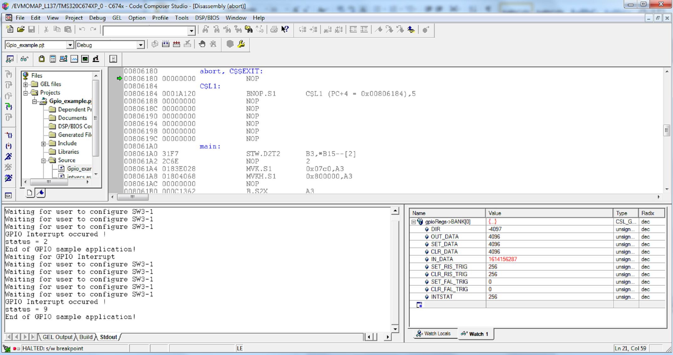
1. I cannot write a value to GPIO registers, such as gpioRegs->BANK[0].CLR_FAL_TRIG, in either the program or watch window.
2. Why SET_RIS_TRIG and CLR_RIS_TRIG have the same value? Should they cancel each other settings (i.e. no interrupt can be acknowledged)? But in fact, the interrupt was acknowledged.
3. Why "status" value becomes 6, instead of 1, when the ISR was executed? I toggled the SW3 position-1 switch only once. Status should increment by only 1 if the ISR is executed only once.
4. I cannot clear INTSTAT register in the watch window. I tried 3 approaches: 1) reload the .out file; 2)Debug->CPU reset; 3)Write 0 to INTSTAT. None of them works.
Thank you for your suggestions in advance !
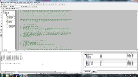
Below are my "Gpio_example.c" code and an output snapshot:
/* ============================================================================
* Copyright (c) Texas Instruments Inc 2002, 2003, 2004, 2005, 2006, 2007
*
* Use of this software is controlled by the terms and conditions found
* in the license agreement under which this software has been supplied.
* ============================================================================
*/
/** ============================================================================
* @brief A simple example to demonstrate CSL GPIO register layer usage
and interrupts in a CSL application.
*
* @file Gpio_example.c
*
* <b> Example Description </b>
* @verbatim
* This example demonstrates the use of GPIO drver/module. The sample does
* this by taking input on GPIO pin GPIO0_8(configured as input pin), via user
* switch SW3-1. This GPIO pin is configured to trigger an interrupt at the
* rising edge. The ISR handler for this interrupt, GPIO_input_isr is called,
* which sets the status variable to 1. Due to this the while loop in the main
* function breaks and blinks led DS1 which is connected to the GPIO0_12
* (configured as output pin).
* @endverbatim
*
*
* <b> Procedure to run the example </b>
* @verbatim
* 1. Open Gpio_example.pjt in CCS
* 2. Build the project
* 3. Connect to target and load the gpio_example.out
* 4. Run the program
* 5. On the console message "Waiting for user to configure SW3-1" is printed
* in a loop
* a. This message occurs until the user intervenes for generating interrupt
* 6. Toggle the user swith SW3-1
* 8. "GPIO Interrupt occured !" message is printed on the console
* a. the movement of switch position causes the GPIO interrupt
* 9. The User LED DS1 now starts blinking (turning on and off at very low freq)
* 10. This is the end of demonstration
* @endverbatim
*
* ============================================================================
**/
#include <stdio.h>
#include <c6x.h>
#include <ti/pspiom/cslr/cslr_gpio.h>
#include <ti/pspiom/cslr/cslr_syscfg_OMAPL137.h>
#include <ti/pspiom/cslr/soc_OMAPL137.h>
#include <ti/pspiom/cslr/cslr_psc_OMAPL137.h>
#include <ti/pspiom/cslr/cslr_intc.h>
/*============================================================================*/
/* GLOBAL VARIABLES */
/*============================================================================*/
/* sys config registers overlay */
CSL_SyscfgRegsOvly sysRegs = (CSL_SyscfgRegsOvly)(CSL_SYSCFG_0_REGS);
/* Psc register overlay */
CSL_PscRegsOvly psc1Regs = (CSL_PscRegsOvly)(CSL_PSC_1_REGS);
/* Gpio register overlay */
CSL_GpioRegsOvly gpioRegs = (CSL_GpioRegsOvly)(CSL_GPIO_0_REGS);
/* Interrupt Controller Register Overlay */
CSL_IntcRegsOvly intcRegs = (CSL_IntcRegsOvly)CSL_INTC_0_REGS;
/*============================================================================*/
/* EXTERNAL FUNCTION PROTOTYPES */
/*============================================================================*/
extern void intcVectorTable(void);
static void delay(Uint32 count);
volatile Int32 status;
#define GPIO0_EVENT 65
#define MAX_BLINK 4
void gpioExample(void)
{
Uint32 ledBlinkCount = 0;
volatile Uint32 temp = 0;
volatile Uint32 pscTimeoutCount = 10240u;
/* Key to be written to enable the pin mux registers for write */
sysRegs->KICK0R = 0x83e70b13;
sysRegs->KICK1R = 0x95A4F1E0;
/* mux between EMA_D8 and GPIO0_8 : enable GPIO0_8 (User Switch - "SW3-1")*/
sysRegs->PINMUX14 = ( (CSL_SYSCFG_PINMUX14_PINMUX14_27_24_GPIO0_8) << \
(CSL_SYSCFG_PINMUX14_PINMUX14_27_24_SHIFT) );
/* mux between EMA_D12 and GPIO0_12 : enable GPIO0_12 (User Led - "DS1") */
sysRegs->PINMUX15 = ( (CSL_SYSCFG_PINMUX15_PINMUX15_11_8_GPIO0_12) << \
(CSL_SYSCFG_PINMUX15_PINMUX15_11_8_SHIFT) );
/* lock the pinmux registers */
sysRegs->KICK0R = 0x00000000;
sysRegs->KICK1R = 0x00000000;
/* Bring the GPIO module out of sleep state */
/* Configure the GPIO Module to Enable state */
psc1Regs->MDCTL[CSL_PSC_GPIO] =
( (psc1Regs->MDCTL[CSL_PSC_GPIO] & 0xFFFFFFE0) | \
CSL_PSC_MDSTAT_STATE_ENABLE );
/* Kick start the Enable Command */
temp = psc1Regs->PTCMD;
temp = ( (temp & CSL_PSC_PTCMD_GO0_MASK) |
(CSL_PSC_PTCMD_GO0_SET << CSL_PSC_PTCMD_GO0_SHIFT) );
psc1Regs->PTCMD |= temp;
/*Wait for the power state transition to occur */
while ( ((psc1Regs->PTSTAT & (CSL_PSC_PTSTAT_GOSTAT0_IN_TRANSITION)) != 0)
&& (pscTimeoutCount>0) )
{
pscTimeoutCount--;
}
/* Check if PSC state transition timed out */
if(pscTimeoutCount == 0)
{
printf("GPIO PSC transition to ON state timed out\n");
return;
}
/* Wait for MODSTAT = ENABLE/DISABLE from LPSC */
pscTimeoutCount = 10240u;
while( ((psc1Regs->MDSTAT[CSL_PSC_GPIO] & (CSL_PSC_MDSTAT_STATE_MASK))
!= CSL_PSC_MDSTAT_STATE_ENABLE) && (pscTimeoutCount>0))
{
pscTimeoutCount--;
}
/* If timeout, the resource may not be functioning */
if (0 == pscTimeoutCount)
{
printf("GPIO Module Enable timed out\n");
return;
}
/* Configure GPIO0_12 (GPIO0_12_PIN) as an output */
gpioRegs->BANK[0].DIR &= ~(CSL_GPIO_DIR_DIR_IN << CSL_GPIO_DIR_DIR12_SHIFT);
/* Configure GPIO0_8 (GPIO0_8_PIN) as an input */
temp = gpioRegs->BANK[0].DIR;
temp = ( (temp & CSL_GPIO_DIR_DIR8_MASK) |
(CSL_GPIO_DIR_DIR_IN << CSL_GPIO_DIR_DIR8_SHIFT) );
gpioRegs->BANK[0].DIR |= temp;
/* Set Data high in SET_DATA register for GPIO(GPIO0_12_PIN). *
* This turns the LED off -see schematic */
temp = gpioRegs->BANK[0].SET_DATA;
temp = ( (temp & CSL_GPIO_SET_DATA_SET12_MASK) |
(CSL_GPIO_SET_DATA_SET_SET << CSL_GPIO_SET_DATA_SET12_SHIFT));
gpioRegs->BANK[0].SET_DATA |= temp;
/* Enable GPIO Bank interrupt for bank 0 */
temp = gpioRegs->BINTEN;
temp = ( (temp & CSL_GPIO_BINTEN_EN0_MASK) |
(CSL_GPIO_BINTEN_EN0_ENABLE << CSL_GPIO_BINTEN_EN0_SHIFT) );
gpioRegs->BINTEN |= temp;
/* Configure GPIO(GPIO0_8_PIN) to generate interrupt on rising edge */
temp = gpioRegs->BANK[0].SET_RIS_TRIG;
temp = ( (temp & CSL_GPIO_SET_RIS_TRIG_SETRIS8_MASK) |
(CSL_GPIO_SET_RIS_TRIG_SETRIS_ENABLE << CSL_GPIO_SET_RIS_TRIG_SETRIS8_SHIFT) );
gpioRegs->BANK[0].SET_RIS_TRIG |= temp;
temp = gpioRegs->BANK[0].CLR_FAL_TRIG;
temp = ( (temp & CSL_GPIO_CLR_FAL_TRIG_CLRFAL8_MASK) |
(0x00000001u << CSL_GPIO_CLR_FAL_TRIG_CLRFAL8_SHIFT) );
gpioRegs->BANK[0].CLR_FAL_TRIG = 256; //|= temp;
gpioRegs->BANK[0].INTSTAT = 0;
/* map GPIO bank 0 event to cpu int4 */
CSL_FINS(intcRegs->INTMUX1, INTC_INTMUX1_INTSEL4,GPIO0_EVENT);
/* set ISTP to point to the vector table address */
ISTP = (unsigned int)intcVectorTable;
/* clear all interrupts, bits 4 thru 15 */
ICR = 0xFFF0;
/* enable the bits for non maskable interrupt and CPUINT4 */
IER = 0x12;
/* enable interrupts, set GIE bit */
_enable_interrupts();
printf("Waiting for GPIO Interrupt\n");
status = 0;
while(status == 0)
{
printf("Waiting for user to configure SW3-1\n");
delay(5000);
}
printf("GPIO Interrupt occured !\n");
printf("status = %ld\n", status);
_disable_interrupts();
while (ledBlinkCount++ < MAX_BLINK)
{
/* Make the GPIO pin (GPIO0_12_PIN) conected to the LED to low. *
* This turns on the LED - see schematic */
temp = gpioRegs->BANK[0].CLR_DATA;
temp = ( (temp & CSL_GPIO_CLR_DATA_CLR12_MASK) |
(CSL_GPIO_CLR_DATA_CLR_CLR << CSL_GPIO_CLR_DATA_CLR12_SHIFT) );
gpioRegs->BANK[0].CLR_DATA |= temp;
delay(2000);
/* Make the GPIO pin (GPIO0_12_PIN) conected to the LED to high *
* This turns the off the LED - see schematic */
temp = gpioRegs->BANK[0].SET_DATA;
temp = ( (temp & CSL_GPIO_SET_DATA_SET12_MASK) |
(CSL_GPIO_SET_DATA_SET_SET << CSL_GPIO_SET_DATA_SET12_SHIFT) );
gpioRegs->BANK[0].SET_DATA |= temp;
delay(2000);
}
printf("End of GPIO sample application!\n");
}
void main (void)
{
gpioExample();
}
interrupt void GPIO_input_isr()
{
/* Let this be here now. I want to see the Heart beat :-) */
status++;
}
/*
* \brief Function to introduce a delay in to the program.
*
* \param count [IN] delay count to wait
* \return None
*
*/
static void delay(Uint32 count)
{
volatile Uint32 tempCount = 0;
volatile Uint32 dummyCount = 0;
for (tempCount = 0; tempCount < count; tempCount++)
{
for (dummyCount = 0; dummyCount < count; dummyCount++)
{
/* dummy loop to wait for some time */
}
}
}