This thread has been locked.

If you have a related question, please click the "Ask a related question" button in the top right corner. The newly created question will be automatically linked to this question.

Issue with L137 GPIO Interrupt

Other Parts Discussed in Thread: STRIKE

I am testing the BIOS PSP GPIO example code and somehow I cannot set it up to generate an interrupt on GPIO falling edge.  The example code is installed at the default directory:

C:\Program Files\Texas Instruments\pspdrivers_01_20_00\packages\ti\pspiom\examples\evmOMAPL137\gpio\src\gpioSample_io.c

The original code will generate an interrupt at rising edge (SW3-1 from 8 to 1) and it works as expected.  However, after I changed it to generate an interrupt on falling edge, it didn't work that way and still can only generates an interrupt on rising edge.  Does anybody have suggestions what I may have done wrong?  Thank you!

The following is what I modified to the original code:


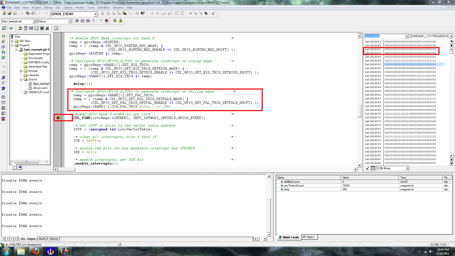
    /* Enable GPIO Bank interrupt for bank GPIO_BANK_0                        */
    Gpio_bankInterruptEnable(gpio0,GPIO_BANK_0);

    /* Configure GPIO(GPIO0_8_PIN) to generate interrupt on rising edge       */
    //Gpio_setRisingEdgeTrigger(gpio0,GPIO0_8_PIN);        Line 118, original code
    Gpio_setFallingEdgeTrigger(gpio0,GPIO0_8_PIN);          Line119, new code
   
    /* Set the interrupt handler for GPIO0_8_PIN. However we cannot register
     * interrupts for individual pins in OMAPL137, therefore  register interrupt
     * for the associated bank(BANK0) as a whole
     */
    UserIntrCmdArg.value = GPIO_BANK_0;

  • Sean,

    Can you set a breakpoint after you set the falling edge trigger and read back the GPIO falling edge trigger register to make sure that it was set correctly?

    -Tommy

  • hi, Tommy, do you know how I can read back the GPIO falling edge register value in BIOSPSP example?  I used the following format, but it seems wrong.

    volatile Int32        temp;

    ...

    temp = *gpio0.deviceInfo.baseAddress.BANK[0].SET_FAL_TRIG;

    Compiling error:  "gpioSample_io.c", line 121: error: expression must have struct or union type

    However, I was able to read back the GPIO falling edge register in the cSLR GPIO example.  I found out I could not modify/write any value to the CLR_FAL_TRIG (Please see my previous post    http://e2e.ti.com/support/dsp/omap_applications_processors/f/42/p/87064/305902.aspx#305902). 

    Each time I changed the example source code, I will recompile the entire project.  But I didn't recompile the drive, since I think no change was done directly to the driver codes.  It has been weeks for me trying to figure out a solution.  Any advice will be greatly appreciated.

  • Sean,

    See if you can read/write the register values directly from the CCS memory view window. 

    -Tommy

  • Normal 0 false false false EN-US ZH-CN X-NONE

    Hi, Tommy, I was able to read back the register via CCS memory window.  I repeated the testing with both the BIOSPSP and cSLR examples. 

    What I found with BIOSPBP was:

    I set the interrupt to be generated at a falling edge:

    1.       Trigger was configured correctly.  Both SET_FAL_TRIG0 and CLF_FAL _TRIG0 bit-8 read 1;

    2.       When I toggle SW3-1 from OFF to ON, it triggered an interrupt.  INTSTAT01 bit-8 read 1;

    3.       However, INTSTAT0 was always 1 indicating that it is a pending interrupt without served.  The ISR didn’t run and LED didn’t blink, flag read 0;

    4.       I cleared the INTSTAT0 and repeated the operations, the ISR was not called;


    I set the interrupt to be generated at rising edge:

    1.       No problem.  All registers read correctly, INTSTAT0 bit-8 red 1 and ISR was called properly;


    I don’t understand how it works, since both falling and rising edge generated an interrupt at exactly the same bit (bit-8) in INTSTAT0.  Why in one case, the interrupt was acknowledged, while the other one the ISR was not called?


    Do you have a L137 EVM on hand?  If so, could you please just give a try?  The only modification was to exchange between the following configurations on Line 119


    Gpio_setRisingEdgeTrigger(gpio0,GPIO0_8_PIN);           // rising edge interrupt

    Or

    Gpio_setFallingEdgeTrigger(gpio0,GPIO0_8_PIN);          // falling edge interrupt

  • What I found with cSLR example was:  I couldn't access to the SET_FAL_TRIG register.  In another words, I cannot configure to generate an interrupt on a falling edge.  Please see the snapshot.

  • Sean,

    I'm afraid that screenshots do not work very well with the forum.  If you could post small code snippets and address/data pairs as text, it would be easier to follow.  For example:

    Code Snippet said:

        GPIO_REGS->BANK[GP0].SET_RIS_TRIG = GP0P11;

    and

    Address = Data said:

    GPIO SET_RIS_TRIG01 (0x01E26024) = 0x00000800

    Since I can't make out your register values, I'm not sure if your code snippet is trying to demonstrate the SET capability of the falling edge trigger or not.  I do see it writing to the CLR register.  Is that intended?

    As far as GPIO operation goes, I have personally used the EVM's GPIO interrupt capabilities on multiple boards.  One thing to be careful of is that the dip switches and GPIO inputs are not debounced.  In other words, if you were to probe the switch signal on a scope as the mechanical switch is manipulated, you should expect to see multiple high/low bounces.  A simple way to "debounce" the signal is simply to wait a predetermined amount of time after an interrupt and then read the GPIO input value to determine what the user intended the value to be.

    -Tommy

  • Normal 0 false false false EN-US ZH-CN X-NONE

    Tommy, no problem, I can post the code snippets and address/data output as text.  Thanks for the reminder of the dip switch denouncing, I was aware of it.  My primary confusion is about the configuration operation to GPIO registers and how the ISR is called.


    I did a test on both “TI cSLR example code” and “TI BIOSPSP example code”.  So in the following, I’ll post the code snippets, and address/data output after the code is executed (i.e., a breakpoint just after the posted code).


    TI cSLR GPIO example:

    Code Snippet said:
    /* Configure GPIO(GPIO0_8_PIN) to generate interrupt on rising edge         */
    temp = gpioRegs->BANK[0].SET_RIS_TRIG;
    temp = ( (temp & CSL_GPIO_SET_RIS_TRIG_SETRIS8_MASK) |
                 (CSL_GPIO_SET_RIS_TRIG_SETRIS_ENABLE << CSL_GPIO_SET_RIS_TRIG_SETRIS8_SHIFT) );
    gpioRegs->BANK[0].SET_RIS_TRIG |= temp;
     
    delay(1);
     
    /* Configure GPIO(GPIO0_8_PIN) to generate interrupt on falling edge         */
    temp = gpioRegs->BANK[0].SET_FAL_TRIG;
    temp = ( (temp & CSL_GPIO_SET_FAL_TRIG_SETFAL8_MASK) |
    (CSL_GPIO_SET_FAL_TRIG_SETFAL_ENABLE << CSL_GPIO_SET_FAL_TRIG_SETFAL8_SHIFT) );
    gpioRegs->BANK[0].CLR_FAL_TRIG =256; //|= temp;


    Address = Data said:
    GPIO SET_RIS_TRIG01 (0x01E26024) = 0x00000800
    GPIO CLR_RIS_TRIG01 (0x01E26028) = 0x00000800
    GPIO SET_FAL_TRIG01 (0x01E2602C) = 0x00000000
    GPIO CLR_RIS_TRIG01 (0x01E26030) = 0x00000000


    My questions are: 

    1.        Why SET_FAL_TRIG was not set correctly?

    2.       Where are     _enable_interrupts() and _disable_interrupts() are defined?


    TI BIOSPSP GPIO example:

    Code Snippet said:
    /* Configure GPIO(GPIO0_8_PIN) to generate interrupt on rising edge       */
    //Gpio_setRisingEdgeTrigger(gpio0,GPIO0_8_PIN);
    Gpio_setFallingEdgeTrigger(gpio0,GPIO0_8_PIN);


    Address = Data said:
    GPIO SET_RIS_TRIG01 (0x01E26024) = 0x00000000
    GPIO CLR_RIS_TRIG01 (0x01E26028) = 0x00000000
    GPIO SET_FAL_TRIG01 (0x01E2602C) = 0x00000800
    GPIO CLR_RIS_TRIG01 (0x01E26030) = 0x00000800
    GPIO INTSTAT01 (0x01E26034) = 0x00000800
    flag = 0


    INTSTAT01 read 1 after SW3-1 toggled from OFF to ON.  My question is: why the GPIO ISR was not called correctly (i.e. flag still 0 instead of 1)?


  • Sean,

    Thanks for posting the snippets and data.

    Sean said:

    1. Why SET_FAL_TRIG was not set correctly?

    I suspect that this may be because your code is writing the 0x100 value to the CLR_FAL_TRIG register instead of the SET_FAL_TRIG register.

    Sean said:

    2. Where are _enable_interrupts() and _disable_interrupts() are defined?

    These are intrinsics supported by the compiler.  There is a brief usage description in the C6x Optimizing Compiler Manual: http://www.ti.com/lit/pdf/spru187

    Sean said:

    INTSTAT01 read 1 after SW3-1 toggled from OFF to ON.  My question is: why the GPIO ISR was not called correctly (i.e. flag still 0 instead of 1)?

    It's difficult to tell what happened here.  Is "flag" a variable that is set by your ISR?


  • Normal 0 false false false EN-US ZH-CN X-NONE

    Tommy, thank you for staying so late to help me figure out the problem.  You are right; it is a bug that I should set the FAL_TRIG instead of clear the register.  Sorry, I shall have done a better check before posting the code here.  Now I manage to make the cSLR code work as I expect, and thank you again for the diagnostics!


    One more question:

    GPIO User Guide says “pending GPIO interrupts are indicated with 1 logic 1 and GPIO interrupts that are not pending are indicated with a logic 0”.  My observation is even the ISR is called and completed, the INTSTAT01 bit is still 1 (i.e. the ISR itself doesn’t automatically clear the INTSTAT01 bit, showing the interrupt is still “pending”).  Do I need to clear the bit before exiting the ISR to ensure next interrupt can be triggered properly?  Such as


    Code Snippet said:
    /* clear all interrupts, bits 4 thru 15                                   */
    ICR = 0xFFF0;
    /* enable the bits for non maskable interrupt and CPUINT4                 */
    IER = 0x12;


  • Sean,

    The GPIO interrupt signal is generated at the bank level.  In other words, all 16 pins in each GPIO bank share one interrupt signal.  Since interrupts can be enabled for each pin, the ISR needs to be able to determine which pin triggered the interrupt.  That's where the INTSTAT comes in with a flag for each "pending" interrupt.

    The interrupt status is not automatically cleared because it is possible for another GPIO pin to generate a new interrupt while the software is servicing an older interrupt from the same bank.  For example, you would not want to clear the entire INTSTAT register when leaving the ISR in the following scenario:

    1. GPIO interrupts are enabled for GP0[5] and GP0[7]
    2. GP0[5] generates an interrupt
    3. Software enters GP0_BANK_ISR() and only sees the GP0[5] interrupt
    4. GP0[7] generates a new interrupt (a new interrupt pulse will be generated for GP0[7])
    5. Software clears INTSTAT flag for GP0[5]
    6. Software exits GP0_BANK_ISR() without ever seeing the GP0[7] interrupt, but will take care of it on the next interrupt

    It is up to the ISR software to clear each pending interrupt in the INTSTAT register as it is processed by writing-1-to-clear.

    I think the IFR clearing is handled by the hardware automatically when it sucessfully handles an interrupt.  You can see this by stepping through your code while monitoring the core registers in CCS.

    -Tommy

  • Thank you, Tommy. 

  • Normal 0 false false false EN-US ZH-CN X-NONE

    Hi, Tommy, I have one more question regarding the cSLR GPIO example code.  Do you remember one of my previous post reported that the ISR seemed running twice with the DIP toggle?  I was not sure if it’s because of the deboucing of  DIP or bugs in my code.  So I modified the ISR to check it out.  The following is how the ISR looks like now:

    Code Snippet said:

    interrupt void GPIO_input_isr(void)

    {

    volatile Uint32 ledBlinkCount;

    volatile Uint32 temp = 0;

    volatile Uint32 flag = 0;


    /*There is significant signal bounce at the GPIO pin connected to the User Switches (SW3). These bounces can generate spurious interrupts (at either falling or rising).  Hence check the steady state (after some delay).  However, in real applications this delay-check may be done outside ISR*/

    delay(6000);


    printf ("1st time flag = %d\n", flag);


    if ( ((gpioRegs->BANK[0].IN_DATA & 0x100u) == 0) && flag == 0)

    {

                    for (ledBlinkCount = 0; ledBlinkCount < 3; ledBlinkCount++) //blink DS1

                    {

                    /* Make the GPIO pin (GPIO0_12_PIN) conected to the LED to low. *

                    * This turns on the LED DS1 - see schematic         */

                    temp = gpioRegs->BANK[0].CLR_DATA;

                    temp = ( (temp & CSL_GPIO_CLR_DATA_CLR12_MASK) |

                    (CSL_GPIO_CLR_DATA_CLR_CLR << CSL_GPIO_CLR_DATA_CLR12_SHIFT) );

                    gpioRegs->BANK[0].CLR_DATA |= temp;


                    delay(2000);


                    /* Make the GPIO pin (GPIO0_12_PIN) conected to the LED to high *

                    * This turns the off the LED DS2 - see schematic    */

                    temp = gpioRegs->BANK[0].SET_DATA;

                                    temp = ( (temp & CSL_GPIO_SET_DATA_SET12_MASK) |

                    (CSL_GPIO_SET_DATA_SET_SET << CSL_GPIO_SET_DATA_SET12_SHIFT) );

                    gpioRegs->BANK[0].SET_DATA |= temp;


                    delay(2000);


                    printf("%d\n", ledBlinkCount);

                    }


                    /* clear corresponding INTSTAT01 interrupt bit */

                    temp = gpioRegs->BANK[0].INTSTAT;

                    temp = temp | 0x100u;

                    gpioRegs->BANK[0].INTSTAT = temp;


                    /* to avoid the ISR running twice (i.e. LED blinks twice) */

                    flag = 0x1u;

    }

    }

    and

    Stdout said:

    Waiting for user to configure SW3-1

    1st time flag = 0

    0

    1

    2

    Waiting for user to configure SW3-1

    :

    :

    :

    Waiting for user to configure SW3-1

    1st time flag = 0

    0

    1

    2

    1st time flag = 0   (<--here is my problem, why the ISR was executed twice?)

    0

    1

    2

    Waiting for user to configure SW3-1

    The above Stdout message was captured when I toggled DIP SW3-1 OFF->ON (Falling edge).  I have added a “delay(6000)”, and the ISR has been executed once.  Why was it executed again?  I also checked the memory 0x01E26034h (INTSTAT01), it toggled (0->1->0) only once (i.e. only one falling edge interrupt was generated).

    As you can see from the Stdout, this problem was not constant either.   

    Any suggestions?  Thank you.

  • Sean,

    I'm not sure if this is causing your extra interrupt, but typical read-modify-write operations should not be used on the SET and CLR registers because the read-back value reflects the programmed output value, but writing a 1 to any bit will initiate the SET or CLR function.

    For example, let's say that GP0[3:0] is configured to output the values 0b0111.  If you read back the SET or CLR registers, they will both read back 0b0111.  Let's say that now you want to clear GP0[0].  The recommended way to do this is to perform a direct write:

    gpioRegs->BANK[0].CLR_DATA = 0x1;

    This will then clear just GP0[0] and GP0[3:0] will output 0b0110.

    If you use a read-modify-write to clear GP0[0], you end up reading back 0b0111 from CLR_DATA[3:0], then binary OR it with 0b0001 (like this: 0b0111 | 0b0001), which produces 0b0111.  Now when you write this value to gpioRegs->BANK[0].CLR_DATA, you end up clearing all of the bits that used to be outputting a logic high and GP0[3:0] outputs 0b0000.

    -Tommy

  • Normal 0 false false false EN-US ZH-CN X-NONE

    Tommy, thanks for the quick response. I apologize if you have received multiple emails since I tested and updated the message for several times.

    I replaced the read-modify-write with your recommended operations, but the extra interrupt was still there.  This is what the new code looks like now:

    interrupt void GPIO_input_isr(void)
    {
        volatile Uint32 ledBlinkCount;  //to delete later
                volatile Uint32 temp = 0;
                volatile Uint32 flag = 0;
     
        /*
        There is significant signal bounce at the GPIO pin connected to the User
        Switches (SW3). These bounces can generate spurious interrupts (at either
        falling or rising). Hence check the steady state (after some delay).
        However, in real applications this delay-check may be done outside ISR
        */
                delay(6000);
               
                printf ("1st time flag = %d\n", flag);
               
                if ( ((gpioRegs->BANK[0].IN_DATA & 0x100u) == 0) && flag == 0)
                {
                for (ledBlinkCount = 0; ledBlinkCount < 3; ledBlinkCount++) //blink DS1
                {
                /* Make the GPIO pin (GPIO0_12_PIN) conected to the LED to low. *
                * This turns on the LED DS1 - see schematic         */
                //temp = gpioRegs->BANK[0].CLR_DATA;
                //temp = ( (temp & CSL_GPIO_CLR_DATA_CLR12_MASK) |
                //          (CSL_GPIO_CLR_DATA_CLR_CLR << CSL_GPIO_CLR_DATA_CLR12_SHIFT) );
                gpioRegs->BANK[0].CLR_DATA = 0x1000u;
     
                delay(2000);
     
                /* Make the GPIO pin (GPIO0_12_PIN) conected to the LED to high *
                * This turns the off the LED DS2 - see schematic    */
                //temp = gpioRegs->BANK[0].SET_DATA;
                            //temp = ( (temp & CSL_GPIO_SET_DATA_SET12_MASK) |
                //          (CSL_GPIO_SET_DATA_SET_SET << CSL_GPIO_SET_DATA_SET12_SHIFT) );
                gpioRegs->BANK[0].SET_DATA= 0x1000u;
     
                delay(2000);
     
                                        printf("ledBlinkCount  = %d\n", ledBlinkCount);
                }
                            /* clear corresponding INTSTAT01 interrupt bit */
                            temp = gpioRegs->BANK[0].INTSTAT;
                            temp = temp | 0x100u;
                gpioRegs->BANK[0].INTSTAT = temp;
     
                            /* to control/avoid the ISR running twice (i.e. LED blinks twice) */
                            flag = 0x1u;
                }
    }

    “printf ("1st time flag = %d\n", flag);” will be executed only when ISR is executed, while “printf("%d\n", ledBlinkCount);” will be executed only when a true falling edge was detected.  As shown below, the ISR was completely executed and then it was executed again IMMEDIATELY.  I also monitored the value of 0x01E26020h (IN_DATA01) and 0x01E26034h (INTSTAT01).  IN_DATA01 Bit-8 and entire INTSTAT01 register were 0 when the ISR was executed for the second time.

    Waiting for user to configure SW3-1
    Waiting for user to configure SW3-1
    1st time flag = 0
    1st time flag = 0                      (<-- printed when ISR was executed)
    ledBlinkCount  = 0                 (<-- printed when a falling edge was detected)
    ledBlinkCount  = 1
    ledBlinkCount  = 2
    1st time flag = 0                      (<-- printed when ISR was executed, immediately)
    ledBlinkCount  = 0
    ledBlinkCount  = 1
    ledBlinkCount  = 2
    Waiting for user to configure SW3-1
    Waiting for user to configure SW3-1


  • Tommy, thanks for the quick response.  I replaced the read-modify-write with your recommended operations, but it seems like the extra interrupt was still there.  This is what the new code looks like now:

    Code Snippet said:

    interrupt void GPIO_input_isr(void)
    {
        volatile Uint32 ledBlinkCount;  //to delete later
        volatile Uint32 temp = 0;
        volatile Uint32 flag = 0;

        delay(6000);
        printf ("1st time flag = %d\n", flag);
        if ( ((gpioRegs->BANK[0].IN_DATA & 0x100u) == 0) && flag == 0)
        {
                for (ledBlinkCount = 0; ledBlinkCount < 3; ledBlinkCount++) //blink DS1
            {
                /* Make the GPIO pin (GPIO0_12_PIN) conected to the LED to low. *
                gpioRegs->BANK[0].CLR_DATA = 0x1000u;
                delay(2000);

                gpioRegs->BANK[0].SET_DATA= 0x1000u;
                delay(2000);
                printf("%d\n", ledBlinkCount);
            }
        /* clear corresponding INTSTAT01 interrupt bit */
        temp = gpioRegs->BANK[0].INTSTAT;
          temp = temp | 0x100u;
        gpioRegs->BANK[0].INTSTAT = temp;

        /* to control/avoid if() executed twice */
        flag = 0x1u;
        }
    }


    “printf ("1st time flag = %d\n", flag);” will be executed only when ISR is executed, while “printf("%d\n", ledBlinkCount);” will be executed only when a true falling edge happens.  As shown below in Stdout, it seems like the ISR was completely executed and then it was executed again IMMEDIATELY.  That’s what confused me.

    Stdout said:

    Waiting for user to configure SW3-1
    Waiting for user to configure SW3-1
    1st time flag = 0
    1st time flag = 0
    0
    1
    2
    1st time flag = 0
    0
    1
    2
    Waiting for user to configure SW3-1
    Waiting for user to configure SW3-1


  • Sean,

    I didn't notice in your previous post, but it looks like you are performing a read-modify-write on the INTSTAT register as well.  This register is write-1-clear (W1C) so it is similar to the CLR register.  By doing the read-modify-write, you are clearing all of the active INTSTAT values at once.  Perhaps it is hiding the source of the second interrupt.

    -Tommy

  • Normal 0 false false false EN-US ZH-CN X-NONE

    Tommy, I changed the read-modify-write operation of INTSTAT, but the extra interrupt was still there.  One question:  assume now I have an interrupt that has already generated 1 in INTSTAT register.  Before this flag bit is cleared (to 0), there comes a second exactly same interrupt.  Will this second interrupt be ignored?  Or will it be stored so that it can be serviced after the first ISR?

  • Sean,

    Good point.  Even when the INTSTAT flag is set, subsequent GPIO activity on the pin will generate additional interrupts to the CPU so it's possible to have an additional interrupt queued up while the pin signal is bouncing in the ISR debouncing wait function.  To see if this is the case, you can disable the GPIO interrupts for that specific pin with the CLR_*_TRIG registers before the debouncing wait function and then reenable it after the wait function.

    If that works, there is still the possibility that a really fast follow-up GPIO bounce can strike between the time that the CPU branches to ISR and when you disable the interrupt.

    -Tommy

  • Tommy, you provided a good approach. I disabled the trigger at the beginning, and renabled it at the last step of the ISR. This way the extra interrupt disappeared.  Regarding the CPU capability to queue up the interrupts, is there anyway to disable this function, or is it always the case for L137?  I truly appreciate your help along my laundry list of questions. 

  • Sean,

    There's not an easy way to disable the queueing of interrupts.  This is typically a desired feature so that high-latency systems will not miss interrupt events.  You might be able to mask GPIO interrupts for a period of time at the interrupt controller level, but that can lead to problems if you are looking for interrupts from multiple pins in the same bank.  The safest thing to do would probably be to disable only a single pin interrupt at a time through the GPIO module and ignore interrupts where INTSTAT is empty.

    -Tommy

  • Tommy, do you know in which document I can find the descriptions of the queueing of interrupts?

  • Sean,

    The interrupt architecture is described in the C674x Megagmodule guide: http://www.ti.com/lit/pdf/sprufk5

    Since you are using a dedicated interrupt line, I think the DSP clears the status flag before entering your ISR.

    -Tommy

  • What is the relationship between IFR, GPIO INTSTAT01, and EVTFLAG65?  Is INTSTAT01 sort of an event-level flag, same as the EVTFLAG65, while IFR is the ultimate DSP CPU INT-level flag to trigger the processing of ISR?

  • Sean,

    INTSTAT01 is local to the GPIO module.  The GPIO module has one interrupt signal per bank.  In the case of BANK0, this signal is hooked up to event 65 in the DSP megamodule's interrupt logic.

    Event 65 is routed per the user's configuration to an actual INT signal in the DSP megamodule (INT4-INT15).  The IFR register reflects the history of the INT signals.

    -Tommy


  • Got it, thank you for your explanation, Tommy.