This thread has been locked.

If you have a related question, please click the "Ask a related question" button in the top right corner. The newly created question will be automatically linked to this question.

66AK2H14: 10G Serdes on-chip BERT testing

Part Number: 66AK2H14

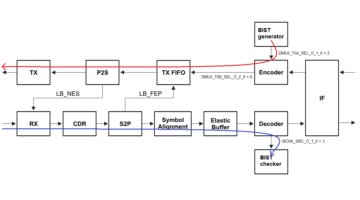
I would like to clarify the TX/RX data paths when BIST Generator and Checker are used in the Diag example in RTOS Processor SDK.

The SerDes User Guide describes some register fields to configure the TX/RX data paths. For the TX data path, DMUX_TXA_SEL_O_1_0 and DMUX_TXB_SEL_O_2_0 in Lane_000. For the RX data path, BCHK_SRC_O_1_0 in Lane_004. The registers are configured for on-chip BERT testing in the source code of the Diag example as follows.

 DMUX_TXA_SEL_O_1_0 = 2 (BIST generator data is passed to the encoder)
 DMUX_TXB_SEL_O_2_0 = 0 (Output of encoder is passed to the TX FIFO)
 BCHK_SRC_O_1_0 = 3 (BIST checker source uses output of reg1 flop bank before Interface blocks)

Serializer/Deserializer (SerDes) for KeyStone II Devices User Guide (Rev. A)
http://www.ti.com/lit/ug/spruho3a/spruho3a.pdf
18.2.1 Lane_000 - Register at 000
18.2.2 Lane_004 - Register at 004

PROCESSOR-SDK-RTOS-K2HK  06_01_00_08
http://software-dl.ti.com/processor-sdk-rtos/esd/K2HK/06_01_00_08/index_FDS.html
\pdk_k2hk_4_0_15\packages\ti\diag\serdes_diag
 \serdes_diag.h
 \test\k2h\c66\bios\serdes_diag_test.c

I understand that the TX/RX data paths when the registers are configured as above are as shown in the figure below.

Is my understanding correct?

The SerDes User Guide describes that 8b/10b encoder/decoder are used.

Are the 64/66B encoder/decoder in PCS-R used for 10G Serdes in on-chip BERT testing?

10 Gigabit Ethernet Switch Subsystem User Guide for KeyStone II Devices
http://www.ti.com/lit/ug/spruhj5/spruhj5.pdf
2.6 PCS-R
"64/66B encoding and decoding with support for all reserved codes and signal
 ordered set for fibre channel use"

All 10GbE Config registers (the starting address is 0x02F00000) are not configured in the source code of RTOS Processor SDK, so the registers remain at their reset values during on-chip BERT testing.

Can the on-chip BERT testing be performed correctly when the registers remain at their reset values?

Best regards,

Daisuke

  • Hi,

    I understand that the TX/RX data paths when the registers are configured as above are as shown in the figure below. Is my understanding correct? ========>Yes, correct.

    Are the 64/66B encoder/decoder in PCS-R used for 10G Serdes in on-chip BERT testing? =====>Not sure, are you doing a device to device test? or a loopback test? On the 10GbE user guide: Figure 1-2 3-port 10 Gigabit Ethernet Switch Sub-module Block Diagram, it shows where the PCS-R locates.

    Can the on-chip BERT testing be performed correctly when the registers remain at their reset values? =====>Yes, I used this BERT on 10GbE and it worked.

    Regards, Eric 

  • Hi Eric-san,

    Thank you for your reply.

    Our customer uses the BIST Generator and Checker to test 10G to/from FPGA. If the 64/66B encoder and decoder are used on the FPGA side, it is an error-free, otherwise an error occurs. So the 64/66B encoder and decoder will be used on K2H side.

    On the other hand, they will try to bypass the encoder and decoder by changing the register configuration on the K2H side as follows.

     DMUX_TXA_SEL_O_1_0 = 0 (Main TX data from SOC interface is passed to the encoder)
     DMUX_TXB_SEL_O_2_0 = 3 (BIST generator data is passed to the TX FIFO)
     BCHK_SRC_O_1_0 = 2 (BIST checker source uses output of RX loopback mux before Decoder and Polbits)

    Should the encoder and decoder be used to BER test 10G SerDes?

    Best regards,

    Daisuke

  • Daisuke,

    Can you draw a diagram how the K2H and FPGA is connected? 

    "If the 64/66B encoder and decoder are used on the FPGA side, it is an error-free, otherwise an error occurs" ========>Why they want to bypass 64/66B encoder and decoder?

    I'm checking with design team if this is possible.

    Regards, Eric

  • The 64/66B encoder/decoder is within the PCSR and not the SERDES.

    The SERDES does not have the ability to encode or decode 64/66B with the PRBS patterns.

    The BER test normally use PRBS31 for 8G and up to accommodate the encoder styles like 64/66B, 128/129B, etc., while below that PRBS7 is sufficient since the encoding tends to be 8B10B.

    The only encoder within the SERDES is a 8B10B encoder and decoder. But it is not ever suggested to perform a BER test encoding the data with such an encoder as it prevents the receiver from ever seeing the stress patterns within the PRBS pattern. PRBS7 pattern has a running distance of 7 bits of '0' or '1' followed by a quick toggle. Adding an encoder would limit the run to 5 bits which is the longest run within the 8B10B encoding. A second issue of encoding the PRBS pattern is that 8B10B is always aligned, that is the only 5 bit patterns are always at the same point within the encode. they cannot be shifted right or left, so the receiver is under tested using 8B10B encoded patterns.

    PRBS31 has a much longer run of zeros and ones followed by a quick toggle, encoding that would render the pattern useless for what it was intended to do, which is to test that the receiver does not drift while receiving a set of ones or zeros.

    PRBS patterns are also odd in length so as to shift the test pattern across all possible power of two boundaries, so if a design is based on a 2, 4 or 8 bit architectures they are still fully tested.

  • Hi Denis-san and Eric-san,

    Thank you for your reply.

    Our customer will bypass the encoder and decoder on both K2H side and FPGA side if the PRBS patterns is used. They will change the registers configuration to bypass the encoder and decoder on K2H side as follows.

     DMUX_TXA_SEL_O_1_0 = 0 (Main TX data from SOC interface is passed to the encoder)
     DMUX_TXB_SEL_O_2_0 = 3 (BIST generator data is passed to the TX FIFO)
     BCHK_SRC_O_1_0 = 2 (BIST checker source uses output of RX loopback mux before Decoder and Polbits)

    They will also change the registers configuration for SGMII and SRIO.

    Is my understanding correct?

    Best regards,

    Daisuke