This thread has been locked.

If you have a related question, please click the "Ask a related question" button in the top right corner. The newly created question will be automatically linked to this question.

AM3352: DDR test fails

Part Number: AM3352

Dear Champs,

My customer has used AM3352 in their product and recently found DDR test fail in below.

They want to check if this failed value can be acceptable to AM3352 or not.

Could you please confirm below values exceed JEDEC spec are acceptable to AM3352? 

Thanks and Best Regards,

SI.

  • SI, have they configured the DDR controller according the to following app note: http://www.ti.com/lit/pdf/sprack4 ?

    What version of software are they using to initialize DDR?

    Regards,

    James

  • Hi James,

    Yes. they have configured the DDR controller according the previous wiki at 4 years before, and they have used it during 4 year without any issue.

    Their Linux Processor SDK is v4.0 and they used SBL in it to initialize DDR.

    Their QA team is checking it now to avoid potential quality issue although there is no issue and found this test failure.

    Thanks and Best Regards,

    SI.

  • SI, some of that information from 4 years ago has been updated in the current app note, and even the programming sequence found in SDK 4.0 has been updated since.  I think they would have to upgrade their software and configuration to help fix the test failures.

    At a minimum they would have to redo the configuration according to the appnote to fix the tDQSS issue.  The other issue may be fixed by a simple patch it they diff with the current SDK and look for the changes associated with EMIF_SDRAM_REF_CTRL_REG register

    Regards,

    James

  • Hi James,

    Thanks for this information.

    I'll check the SW changes and will discuss with customer.

    BTW, is it possible to estimate how impact this failure on AM3352? Do you think this is critical?

    Actually my customer is concerning about the test fail of '/Reset rise to CKE rise'. They can accept 'tDQSS' test fail as they can assume it is measurement error.

    Could you please let me know your opinion how the '/Reset rise to CKE rise' is critical to AM3352? 

    Thanks and Best Regards,

    SI.
  • HI SI, I think the reset to CKE violation could potentially cause a boot failure, as you are not giving enough time for the reset to propagate through the memory. 

    I checked the SPL code, and i think this is actually easily fixed with the following code change in  arch/arm/mach-omap2/am33xx/ddr.c

    if (regs->zq_config) {

    writel(0x00003100, &emif_reg[nr]->emif_sdram_ref_ctrl);  /*add this line*/
        

    writel(regs->zq_config, &emif_reg[nr]->emif_zq_config);
    writel(regs->sdram_config, &cstat->secure_emif_sdram_config);
    writel(regs->sdram_config, &emif_reg[nr]->emif_sdram_config);

        /* Trigger initialization */
        /*writel(0x00003100, &emif_reg[nr]->emif_sdram_ref_ctrl);*/  /*comment out this line*/
        /* Wait 1ms because of L3 timeout error */
        udelay(1000);

        /* Write proper sdram_ref_cref_ctrl value */
        writel(regs->ref_ctrl, &emif_reg[nr]->emif_sdram_ref_ctrl);
        writel(regs->ref_ctrl, &emif_reg[nr]->emif_sdram_ref_ctrl_shdw);
    }

    This should give the proper reset timing for the EMIF initialization, which is kicked off by the write to emif_sdram_config.

    Regards,

    James

  • Hi James,

    Do you mean SPL  of LInux?

    Could you please explain more details which register is related with controlling '/Reset rise to CKE rise' value in above?

     Is  'EMIF4D_SDRAM_REFRESH_CTRL' of EMIF register related with '/Reset rise to CKE rise' value? 

    I found 'EMIF_SDRAM_REF_CTRL_REG' is in the SBL of TI-RTOS PDK only, and I found similar structure element 'emif_sdram_ref_ctrl' in the SPL source. I found 'emif_sdram_ref_ctrl' in the 2 files(arch/arm/omap2/am335x/ddr.c, arch/arm/omap2/emif-common.c), but could not find any difference with latest version.(between 4.0 and 6.1) and could not find what is the patch you mentioned.

    It would be very helpful if you can check it and provide more details on this.

    I attached ddr.c and emif-common.c file of SDK4.0.

    Could you please explain what is '/Reset rise to CKE rise' as I have no idea what it is?

    When I checked TRM of AM3352, I assumed 'EMIF_SDRAM_REF_CTRL_REG' is 'EMIF4D_SDRAM_REFRESH_CTRL' of EMIF register and there is only values for self-refresh of DDR memory.

    If  'EMIF_SDRAM_REF_CTRL_REG' is a register affecting on the value of  '/Reset rise to CKE rise', do you think it is ok to control it manually?

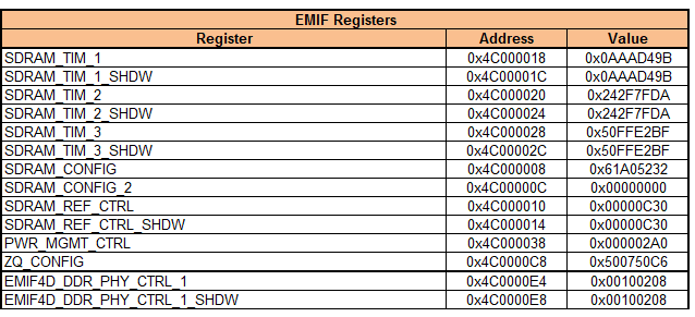
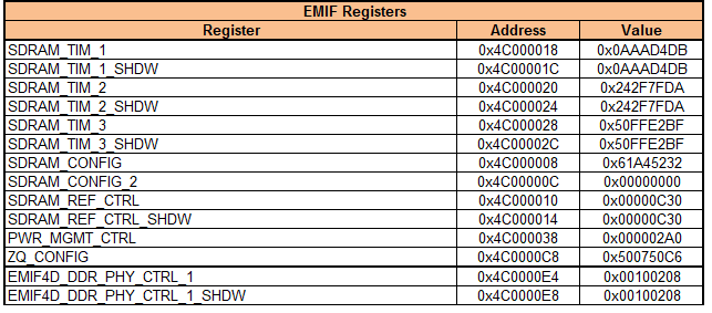
    I tried to calculated EMIF values using latest application notes(sprack4.pdf), and found there were difference in the EMIF timing values, but there was no difference in the EMIF_SDREF value.(both are '0x0000 0C30')

    So, I'm afraid there was no difference in '/Reset rise to CKE rise' even when we modified timing values of EMIF.

    The DDR3 memory is K4B1G1646I-BCMA in below.

    https://www.samsung.com/semiconductor/global.semi/file/resource/2017/11/DS_K4B1G1646I-BC_Rev1_1-0.pdf

    I got the new value as below

    The below is SPL source of Linux PSDK 4.0 for your reference.

    /*
     * DDR Configuration for AM33xx devices.
     *
     * Copyright (C) 2011 Texas Instruments Incorporated - http://www.ti.com/
     *
     * SPDX-License-Identifier:	GPL-2.0+
     */
    
    #include <asm/arch/cpu.h>
    #include <asm/arch/ddr_defs.h>
    #include <asm/arch/sys_proto.h>
    #include <asm/io.h>
    #include <asm/emif.h>
    
    /**
     * Base address for EMIF instances
     */
    static struct emif_reg_struct *emif_reg[2] = {
    				(struct emif_reg_struct *)EMIF4_0_CFG_BASE,
    				(struct emif_reg_struct *)EMIF4_1_CFG_BASE};
    
    /**
     * Base addresses for DDR PHY cmd/data regs
     */
    static struct ddr_cmd_regs *ddr_cmd_reg[2] = {
    				(struct ddr_cmd_regs *)DDR_PHY_CMD_ADDR,
    				(struct ddr_cmd_regs *)DDR_PHY_CMD_ADDR2};
    
    static struct ddr_data_regs *ddr_data_reg[2] = {
    				(struct ddr_data_regs *)DDR_PHY_DATA_ADDR,
    				(struct ddr_data_regs *)DDR_PHY_DATA_ADDR2};
    
    /**
     * Base address for ddr io control instances
     */
    static struct ddr_cmdtctrl *ioctrl_reg = {
    			(struct ddr_cmdtctrl *)DDR_CONTROL_BASE_ADDR};
    
    static inline u32 get_mr(int nr, u32 cs, u32 mr_addr)
    {
    	u32 mr;
    
    	mr_addr |= cs << EMIF_REG_CS_SHIFT;
    	writel(mr_addr, &emif_reg[nr]->emif_lpddr2_mode_reg_cfg);
    
    	mr = readl(&emif_reg[nr]->emif_lpddr2_mode_reg_data);
    	debug("get_mr: EMIF1 cs %d mr %08x val 0x%x\n", cs, mr_addr, mr);
    	if (((mr & 0x0000ff00) >>  8) == (mr & 0xff) &&
    	    ((mr & 0x00ff0000) >> 16) == (mr & 0xff) &&
    	    ((mr & 0xff000000) >> 24) == (mr & 0xff))
    		return mr & 0xff;
    	else
    		return mr;
    }
    
    static inline void set_mr(int nr, u32 cs, u32 mr_addr, u32 mr_val)
    {
    	mr_addr |= cs << EMIF_REG_CS_SHIFT;
    	writel(mr_addr, &emif_reg[nr]->emif_lpddr2_mode_reg_cfg);
    	writel(mr_val, &emif_reg[nr]->emif_lpddr2_mode_reg_data);
    }
    
    static void configure_mr(int nr, u32 cs)
    {
    	u32 mr_addr;
    
    	while (get_mr(nr, cs, LPDDR2_MR0) & LPDDR2_MR0_DAI_MASK)
    		;
    	set_mr(nr, cs, LPDDR2_MR10, 0x56);
    
    	set_mr(nr, cs, LPDDR2_MR1, 0x43);
    	set_mr(nr, cs, LPDDR2_MR2, 0x2);
    
    	mr_addr = LPDDR2_MR2 | EMIF_REG_REFRESH_EN_MASK;
    	set_mr(nr, cs, mr_addr, 0x2);
    }
    
    /*
     * Configure EMIF4D5 registers and MR registers For details about these magic
     * values please see the EMIF registers section of the TRM.
     */
    void config_sdram_emif4d5(const struct emif_regs *regs, int nr)
    {
    	writel(0xA0, &emif_reg[nr]->emif_pwr_mgmt_ctrl);
    	writel(0xA0, &emif_reg[nr]->emif_pwr_mgmt_ctrl_shdw);
    	writel(regs->zq_config, &emif_reg[nr]->emif_zq_config);
    
    	writel(regs->temp_alert_config, &emif_reg[nr]->emif_temp_alert_config);
    	writel(regs->emif_rd_wr_lvl_rmp_win,
    	       &emif_reg[nr]->emif_rd_wr_lvl_rmp_win);
    	writel(regs->emif_rd_wr_lvl_rmp_ctl,
    	       &emif_reg[nr]->emif_rd_wr_lvl_rmp_ctl);
    	writel(regs->emif_rd_wr_lvl_ctl, &emif_reg[nr]->emif_rd_wr_lvl_ctl);
    	writel(regs->emif_rd_wr_exec_thresh,
    	       &emif_reg[nr]->emif_rd_wr_exec_thresh);
    
    	/*
    	 * for most SOCs these registers won't need to be changed so only
    	 * write to these registers if someone explicitly has set the
    	 * register's value.
    	 */
    	if(regs->emif_cos_config) {
    		writel(regs->emif_prio_class_serv_map, &emif_reg[nr]->emif_prio_class_serv_map);
    		writel(regs->emif_connect_id_serv_1_map, &emif_reg[nr]->emif_connect_id_serv_1_map);
    		writel(regs->emif_connect_id_serv_2_map, &emif_reg[nr]->emif_connect_id_serv_2_map);
    		writel(regs->emif_cos_config, &emif_reg[nr]->emif_cos_config);
    	}
    
    	/*
    	 * Sequence to ensure that the PHY is in a known state prior to
    	 * startting hardware leveling.  Also acts as to latch some state from
    	 * the EMIF into the PHY.
    	 */
    	writel(0x2011, &emif_reg[nr]->emif_iodft_tlgc);
    	writel(0x2411, &emif_reg[nr]->emif_iodft_tlgc);
    	writel(0x2011, &emif_reg[nr]->emif_iodft_tlgc);
    
    	clrbits_le32(&emif_reg[nr]->emif_sdram_ref_ctrl,
    			EMIF_REG_INITREF_DIS_MASK);
    
    	writel(regs->sdram_config, &emif_reg[nr]->emif_sdram_config);
    	writel(regs->sdram_config, &cstat->secure_emif_sdram_config);
    
    	/* Wait 1ms because of L3 timeout error */
    	udelay(1000);
    
    	writel(regs->ref_ctrl, &emif_reg[nr]->emif_sdram_ref_ctrl);
    	writel(regs->ref_ctrl, &emif_reg[nr]->emif_sdram_ref_ctrl_shdw);
    
    	/* Perform hardware leveling for DDR3 */
    	if (emif_sdram_type(regs->sdram_config) == EMIF_SDRAM_TYPE_DDR3) {
    		writel(readl(&emif_reg[nr]->emif_ddr_ext_phy_ctrl_36) |
    		       0x100, &emif_reg[nr]->emif_ddr_ext_phy_ctrl_36);
    		writel(readl(&emif_reg[nr]->emif_ddr_ext_phy_ctrl_36_shdw) |
    		       0x100, &emif_reg[nr]->emif_ddr_ext_phy_ctrl_36_shdw);
    
    		writel(0x80000000, &emif_reg[nr]->emif_rd_wr_lvl_rmp_ctl);
    
    		/* Enable read leveling */
    		writel(0x80000000, &emif_reg[nr]->emif_rd_wr_lvl_ctl);
    
    		/*
    		 * Enable full read and write leveling.  Wait for read and write
    		 * leveling bit to clear RDWRLVLFULL_START bit 31
    		 */
    		while ((readl(&emif_reg[nr]->emif_rd_wr_lvl_ctl) & 0x80000000)
    		      != 0)
    			;
    
    		/* Check the timeout register to see if leveling is complete */
    		if ((readl(&emif_reg[nr]->emif_status) & 0x70) != 0)
    			puts("DDR3 H/W leveling incomplete with errors\n");
    
    	} else {
    		/* DDR2 */
    		configure_mr(nr, 0);
    		configure_mr(nr, 1);
    	}
    }
    
    /**
     * Configure SDRAM
     */
    void config_sdram(const struct emif_regs *regs, int nr)
    {
    	if (regs->zq_config) {
    		writel(regs->zq_config, &emif_reg[nr]->emif_zq_config);
    		writel(regs->sdram_config, &cstat->secure_emif_sdram_config);
    		writel(regs->sdram_config, &emif_reg[nr]->emif_sdram_config);
    
    		/* Trigger initialization */
    		writel(0x00003100, &emif_reg[nr]->emif_sdram_ref_ctrl);
    		/* Wait 1ms because of L3 timeout error */
    		udelay(1000);
    
    		/* Write proper sdram_ref_cref_ctrl value */
    		writel(regs->ref_ctrl, &emif_reg[nr]->emif_sdram_ref_ctrl);
    		writel(regs->ref_ctrl, &emif_reg[nr]->emif_sdram_ref_ctrl_shdw);
    	}
    	writel(regs->ref_ctrl, &emif_reg[nr]->emif_sdram_ref_ctrl);
    	writel(regs->ref_ctrl, &emif_reg[nr]->emif_sdram_ref_ctrl_shdw);
    	writel(regs->sdram_config, &emif_reg[nr]->emif_sdram_config);
    
    	/* Write REG_COS_COUNT_1, REG_COS_COUNT_2, and REG_PR_OLD_COUNT. */
    	if (regs->ocp_config)
    		writel(regs->ocp_config, &emif_reg[nr]->emif_l3_config);
    }
    
    /**
     * Set SDRAM timings
     */
    void set_sdram_timings(const struct emif_regs *regs, int nr)
    {
    	writel(regs->sdram_tim1, &emif_reg[nr]->emif_sdram_tim_1);
    	writel(regs->sdram_tim1, &emif_reg[nr]->emif_sdram_tim_1_shdw);
    	writel(regs->sdram_tim2, &emif_reg[nr]->emif_sdram_tim_2);
    	writel(regs->sdram_tim2, &emif_reg[nr]->emif_sdram_tim_2_shdw);
    	writel(regs->sdram_tim3, &emif_reg[nr]->emif_sdram_tim_3);
    	writel(regs->sdram_tim3, &emif_reg[nr]->emif_sdram_tim_3_shdw);
    }
    
    /*
     * Configure EXT PHY registers for software leveling
     */
    static void ext_phy_settings_swlvl(const struct emif_regs *regs, int nr)
    {
    	u32 *ext_phy_ctrl_base = 0;
    	u32 *emif_ext_phy_ctrl_base = 0;
    	__maybe_unused const u32 *ext_phy_ctrl_const_regs;
    	u32 i = 0;
    	__maybe_unused u32 size;
    
    	ext_phy_ctrl_base = (u32 *)&(regs->emif_ddr_ext_phy_ctrl_1);
    	emif_ext_phy_ctrl_base =
    			(u32 *)&(emif_reg[nr]->emif_ddr_ext_phy_ctrl_1);
    
    	/* Configure external phy control timing registers */
    	for (i = 0; i < EMIF_EXT_PHY_CTRL_TIMING_REG; i++) {
    		writel(*ext_phy_ctrl_base, emif_ext_phy_ctrl_base++);
    		/* Update shadow registers */
    		writel(*ext_phy_ctrl_base++, emif_ext_phy_ctrl_base++);
    	}
    
    #ifdef CONFIG_AM43XX
    	/*
    	 * External phy 6-24 registers do not change with ddr frequency.
    	 * These only need to be set on DDR2 on AM43xx.
    	 */
    	emif_get_ext_phy_ctrl_const_regs(&ext_phy_ctrl_const_regs, &size);
    
    	if (!size)
    		return;
    
    	for (i = 0; i < size; i++) {
    		writel(ext_phy_ctrl_const_regs[i], emif_ext_phy_ctrl_base++);
    		/* Update shadow registers */
    		writel(ext_phy_ctrl_const_regs[i], emif_ext_phy_ctrl_base++);
    	}
    #endif
    }
    
    /*
     * Configure EXT PHY registers for hardware leveling
     */
    static void ext_phy_settings_hwlvl(const struct emif_regs *regs, int nr)
    {
    	/*
    	 * Enable hardware leveling on the EMIF.  For details about these
    	 * magic values please see the EMIF registers section of the TRM.
    	 */
    	writel(0x08020080, &emif_reg[nr]->emif_ddr_ext_phy_ctrl_1);
    	writel(0x08020080, &emif_reg[nr]->emif_ddr_ext_phy_ctrl_1_shdw);
    	writel(0x00000000, &emif_reg[nr]->emif_ddr_ext_phy_ctrl_22);
    	writel(0x00000000, &emif_reg[nr]->emif_ddr_ext_phy_ctrl_22_shdw);
    	writel(0x00600020, &emif_reg[nr]->emif_ddr_ext_phy_ctrl_23);
    	writel(0x00600020, &emif_reg[nr]->emif_ddr_ext_phy_ctrl_23_shdw);
    	writel(0x40010080, &emif_reg[nr]->emif_ddr_ext_phy_ctrl_24);
    	writel(0x40010080, &emif_reg[nr]->emif_ddr_ext_phy_ctrl_24_shdw);
    	writel(0x08102040, &emif_reg[nr]->emif_ddr_ext_phy_ctrl_25);
    	writel(0x08102040, &emif_reg[nr]->emif_ddr_ext_phy_ctrl_25_shdw);
    	writel(0x00200020, &emif_reg[nr]->emif_ddr_ext_phy_ctrl_26);
    	writel(0x00200020, &emif_reg[nr]->emif_ddr_ext_phy_ctrl_26_shdw);
    	writel(0x00200020, &emif_reg[nr]->emif_ddr_ext_phy_ctrl_27);
    	writel(0x00200020, &emif_reg[nr]->emif_ddr_ext_phy_ctrl_27_shdw);
    	writel(0x00200020, &emif_reg[nr]->emif_ddr_ext_phy_ctrl_28);
    	writel(0x00200020, &emif_reg[nr]->emif_ddr_ext_phy_ctrl_28_shdw);
    	writel(0x00200020, &emif_reg[nr]->emif_ddr_ext_phy_ctrl_29);
    	writel(0x00200020, &emif_reg[nr]->emif_ddr_ext_phy_ctrl_29_shdw);
    	writel(0x00200020, &emif_reg[nr]->emif_ddr_ext_phy_ctrl_30);
    	writel(0x00200020, &emif_reg[nr]->emif_ddr_ext_phy_ctrl_30_shdw);
    	writel(0x00000000, &emif_reg[nr]->emif_ddr_ext_phy_ctrl_31);
    	writel(0x00000000, &emif_reg[nr]->emif_ddr_ext_phy_ctrl_31_shdw);
    	writel(0x00000000, &emif_reg[nr]->emif_ddr_ext_phy_ctrl_32);
    	writel(0x00000000, &emif_reg[nr]->emif_ddr_ext_phy_ctrl_32_shdw);
    	writel(0x00000000, &emif_reg[nr]->emif_ddr_ext_phy_ctrl_33);
    	writel(0x00000000, &emif_reg[nr]->emif_ddr_ext_phy_ctrl_33_shdw);
    	writel(0x00000000, &emif_reg[nr]->emif_ddr_ext_phy_ctrl_34);
    	writel(0x00000000, &emif_reg[nr]->emif_ddr_ext_phy_ctrl_34_shdw);
    	writel(0x00000000, &emif_reg[nr]->emif_ddr_ext_phy_ctrl_35);
    	writel(0x00000000, &emif_reg[nr]->emif_ddr_ext_phy_ctrl_35_shdw);
    	writel(0x000000FF, &emif_reg[nr]->emif_ddr_ext_phy_ctrl_36);
    	writel(0x000000FF, &emif_reg[nr]->emif_ddr_ext_phy_ctrl_36_shdw);
    
    	/*
    	 * Sequence to ensure that the PHY is again in a known state after
    	 * hardware leveling.
    	 */
    	writel(0x2011, &emif_reg[nr]->emif_iodft_tlgc);
    	writel(0x2411, &emif_reg[nr]->emif_iodft_tlgc);
    	writel(0x2011, &emif_reg[nr]->emif_iodft_tlgc);
    }
    
    /**
     * Configure DDR PHY
     */
    void config_ddr_phy(const struct emif_regs *regs, int nr)
    {
    	/*
    	 * Disable initialization and refreshes for now until we finish
    	 * programming EMIF regs and set time between rising edge of
    	 * DDR_RESET to rising edge of DDR_CKE to > 500us per memory spec.
    	 * We currently hardcode a value based on a max expected frequency
    	 * of 400MHz.
    	 */
    	writel(EMIF_REG_INITREF_DIS_MASK | 0x3100,
    		&emif_reg[nr]->emif_sdram_ref_ctrl);
    
    	writel(regs->emif_ddr_phy_ctlr_1,
    		&emif_reg[nr]->emif_ddr_phy_ctrl_1);
    	writel(regs->emif_ddr_phy_ctlr_1,
    		&emif_reg[nr]->emif_ddr_phy_ctrl_1_shdw);
    
    	if (get_emif_rev((u32)emif_reg[nr]) == EMIF_4D5) {
    		if (emif_sdram_type(regs->sdram_config) == EMIF_SDRAM_TYPE_DDR3)
    			ext_phy_settings_hwlvl(regs, nr);
    		else
    			ext_phy_settings_swlvl(regs, nr);
    	}
    }
    
    /**
     * Configure DDR CMD control registers
     */
    void config_cmd_ctrl(const struct cmd_control *cmd, int nr)
    {
    	if (!cmd)
    		return;
    
    	writel(cmd->cmd0csratio, &ddr_cmd_reg[nr]->cm0csratio);
    	writel(cmd->cmd0iclkout, &ddr_cmd_reg[nr]->cm0iclkout);
    
    	writel(cmd->cmd1csratio, &ddr_cmd_reg[nr]->cm1csratio);
    	writel(cmd->cmd1iclkout, &ddr_cmd_reg[nr]->cm1iclkout);
    
    	writel(cmd->cmd2csratio, &ddr_cmd_reg[nr]->cm2csratio);
    	writel(cmd->cmd2iclkout, &ddr_cmd_reg[nr]->cm2iclkout);
    }
    
    /**
     * Configure DDR DATA registers
     */
    void config_ddr_data(const struct ddr_data *data, int nr)
    {
    	int i;
    
    	if (!data)
    		return;
    
    	for (i = 0; i < DDR_DATA_REGS_NR; i++) {
    		writel(data->datardsratio0,
    			&(ddr_data_reg[nr]+i)->dt0rdsratio0);
    		writel(data->datawdsratio0,
    			&(ddr_data_reg[nr]+i)->dt0wdsratio0);
    		writel(data->datawiratio0,
    			&(ddr_data_reg[nr]+i)->dt0wiratio0);
    		writel(data->datagiratio0,
    			&(ddr_data_reg[nr]+i)->dt0giratio0);
    		writel(data->datafwsratio0,
    			&(ddr_data_reg[nr]+i)->dt0fwsratio0);
    		writel(data->datawrsratio0,
    			&(ddr_data_reg[nr]+i)->dt0wrsratio0);
    	}
    }
    
    void config_io_ctrl(const struct ctrl_ioregs *ioregs)
    {
    	if (!ioregs)
    		return;
    
    	writel(ioregs->cm0ioctl, &ioctrl_reg->cm0ioctl);
    	writel(ioregs->cm1ioctl, &ioctrl_reg->cm1ioctl);
    	writel(ioregs->cm2ioctl, &ioctrl_reg->cm2ioctl);
    	writel(ioregs->dt0ioctl, &ioctrl_reg->dt0ioctl);
    	writel(ioregs->dt1ioctl, &ioctrl_reg->dt1ioctl);
    #ifdef CONFIG_AM43XX
    	writel(ioregs->dt2ioctrl, &ioctrl_reg->dt2ioctrl);
    	writel(ioregs->dt3ioctrl, &ioctrl_reg->dt3ioctrl);
    	writel(ioregs->emif_sdram_config_ext,
    	       &ioctrl_reg->emif_sdram_config_ext);
    #endif
    }
    

    /*
     * EMIF programming
     *
     * (C) Copyright 2010
     * Texas Instruments, <www.ti.com>
     *
     * Aneesh V <aneesh@ti.com>
     *
     * SPDX-License-Identifier:	GPL-2.0+
     */
    
    #include <common.h>
    #include <asm/emif.h>
    #include <asm/arch/clock.h>
    #include <asm/arch/sys_proto.h>
    #include <asm/omap_common.h>
    #include <asm/omap_sec_common.h>
    #include <asm/utils.h>
    #include <linux/compiler.h>
    
    static int emif1_enabled = -1, emif2_enabled = -1;
    
    void set_lpmode_selfrefresh(u32 base)
    {
    	struct emif_reg_struct *emif = (struct emif_reg_struct *)base;
    	u32 reg;
    
    	reg = readl(&emif->emif_pwr_mgmt_ctrl);
    	reg &= ~EMIF_REG_LP_MODE_MASK;
    	reg |= LP_MODE_SELF_REFRESH << EMIF_REG_LP_MODE_SHIFT;
    	reg &= ~EMIF_REG_SR_TIM_MASK;
    	writel(reg, &emif->emif_pwr_mgmt_ctrl);
    
    	/* dummy read for the new SR_TIM to be loaded */
    	readl(&emif->emif_pwr_mgmt_ctrl);
    }
    
    void force_emif_self_refresh()
    {
    	set_lpmode_selfrefresh(EMIF1_BASE);
    	if (!is_dra72x())
    		set_lpmode_selfrefresh(EMIF2_BASE);
    }
    
    inline u32 emif_num(u32 base)
    {
    	if (base == EMIF1_BASE)
    		return 1;
    	else if (base == EMIF2_BASE)
    		return 2;
    	else
    		return 0;
    }
    
    static inline u32 get_mr(u32 base, u32 cs, u32 mr_addr)
    {
    	u32 mr;
    	struct emif_reg_struct *emif = (struct emif_reg_struct *)base;
    
    	mr_addr |= cs << EMIF_REG_CS_SHIFT;
    	writel(mr_addr, &emif->emif_lpddr2_mode_reg_cfg);
    	if (omap_revision() == OMAP4430_ES2_0)
    		mr = readl(&emif->emif_lpddr2_mode_reg_data_es2);
    	else
    		mr = readl(&emif->emif_lpddr2_mode_reg_data);
    	debug("get_mr: EMIF%d cs %d mr %08x val 0x%x\n", emif_num(base),
    	      cs, mr_addr, mr);
    	if (((mr & 0x0000ff00) >>  8) == (mr & 0xff) &&
    	    ((mr & 0x00ff0000) >> 16) == (mr & 0xff) &&
    	    ((mr & 0xff000000) >> 24) == (mr & 0xff))
    		return mr & 0xff;
    	else
    		return mr;
    }
    
    static inline void set_mr(u32 base, u32 cs, u32 mr_addr, u32 mr_val)
    {
    	struct emif_reg_struct *emif = (struct emif_reg_struct *)base;
    
    	mr_addr |= cs << EMIF_REG_CS_SHIFT;
    	writel(mr_addr, &emif->emif_lpddr2_mode_reg_cfg);
    	writel(mr_val, &emif->emif_lpddr2_mode_reg_data);
    }
    
    void emif_reset_phy(u32 base)
    {
    	struct emif_reg_struct *emif = (struct emif_reg_struct *)base;
    	u32 iodft;
    
    	iodft = readl(&emif->emif_iodft_tlgc);
    	iodft |= EMIF_REG_RESET_PHY_MASK;
    	writel(iodft, &emif->emif_iodft_tlgc);
    }
    
    static void do_lpddr2_init(u32 base, u32 cs)
    {
    	u32 mr_addr;
    	const struct lpddr2_mr_regs *mr_regs;
    
    	get_lpddr2_mr_regs(&mr_regs);
    	/* Wait till device auto initialization is complete */
    	while (get_mr(base, cs, LPDDR2_MR0) & LPDDR2_MR0_DAI_MASK)
    		;
    	set_mr(base, cs, LPDDR2_MR10, mr_regs->mr10);
    	/*
    	 * tZQINIT = 1 us
    	 * Enough loops assuming a maximum of 2GHz
    	 */
    
    	sdelay(2000);
    
    	set_mr(base, cs, LPDDR2_MR1, mr_regs->mr1);
    	set_mr(base, cs, LPDDR2_MR16, mr_regs->mr16);
    
    	/*
    	 * Enable refresh along with writing MR2
    	 * Encoding of RL in MR2 is (RL - 2)
    	 */
    	mr_addr = LPDDR2_MR2 | EMIF_REG_REFRESH_EN_MASK;
    	set_mr(base, cs, mr_addr, mr_regs->mr2);
    
    	if (mr_regs->mr3 > 0)
    		set_mr(base, cs, LPDDR2_MR3, mr_regs->mr3);
    }
    
    static void lpddr2_init(u32 base, const struct emif_regs *regs)
    {
    	struct emif_reg_struct *emif = (struct emif_reg_struct *)base;
    
    	/* Not NVM */
    	clrbits_le32(&emif->emif_lpddr2_nvm_config, EMIF_REG_CS1NVMEN_MASK);
    
    	/*
    	 * Keep REG_INITREF_DIS = 1 to prevent re-initialization of SDRAM
    	 * when EMIF_SDRAM_CONFIG register is written
    	 */
    	setbits_le32(&emif->emif_sdram_ref_ctrl, EMIF_REG_INITREF_DIS_MASK);
    
    	/*
    	 * Set the SDRAM_CONFIG and PHY_CTRL for the
    	 * un-locked frequency & default RL
    	 */
    	writel(regs->sdram_config_init, &emif->emif_sdram_config);
    	writel(regs->emif_ddr_phy_ctlr_1_init, &emif->emif_ddr_phy_ctrl_1);
    
    	do_ext_phy_settings(base, regs);
    
    	do_lpddr2_init(base, CS0);
    	if (regs->sdram_config & EMIF_REG_EBANK_MASK)
    		do_lpddr2_init(base, CS1);
    
    	writel(regs->sdram_config, &emif->emif_sdram_config);
    	writel(regs->emif_ddr_phy_ctlr_1, &emif->emif_ddr_phy_ctrl_1);
    
    	/* Enable refresh now */
    	clrbits_le32(&emif->emif_sdram_ref_ctrl, EMIF_REG_INITREF_DIS_MASK);
    
    	}
    
    __weak void do_ext_phy_settings(u32 base, const struct emif_regs *regs)
    {
    }
    
    void emif_update_timings(u32 base, const struct emif_regs *regs)
    {
    	struct emif_reg_struct *emif = (struct emif_reg_struct *)base;
    
    	if (!is_dra7xx())
    		writel(regs->ref_ctrl, &emif->emif_sdram_ref_ctrl_shdw);
    	else
    		writel(regs->ref_ctrl_final, &emif->emif_sdram_ref_ctrl_shdw);
    
    	writel(regs->sdram_tim1, &emif->emif_sdram_tim_1_shdw);
    	writel(regs->sdram_tim2, &emif->emif_sdram_tim_2_shdw);
    	writel(regs->sdram_tim3, &emif->emif_sdram_tim_3_shdw);
    	if (omap_revision() == OMAP4430_ES1_0) {
    		/* ES1 bug EMIF should be in force idle during freq_update */
    		writel(0, &emif->emif_pwr_mgmt_ctrl);
    	} else {
    		writel(EMIF_PWR_MGMT_CTRL, &emif->emif_pwr_mgmt_ctrl);
    		writel(EMIF_PWR_MGMT_CTRL_SHDW, &emif->emif_pwr_mgmt_ctrl_shdw);
    	}
    	writel(regs->read_idle_ctrl, &emif->emif_read_idlectrl_shdw);
    	writel(regs->zq_config, &emif->emif_zq_config);
    	writel(regs->temp_alert_config, &emif->emif_temp_alert_config);
    	writel(regs->emif_ddr_phy_ctlr_1, &emif->emif_ddr_phy_ctrl_1_shdw);
    
    	if ((omap_revision() >= OMAP5430_ES1_0) || is_dra7xx()) {
    		writel(EMIF_L3_CONFIG_VAL_SYS_10_MPU_5_LL_0,
    			&emif->emif_l3_config);
    	} else if (omap_revision() >= OMAP4460_ES1_0) {
    		writel(EMIF_L3_CONFIG_VAL_SYS_10_MPU_3_LL_0,
    			&emif->emif_l3_config);
    	} else {
    		writel(EMIF_L3_CONFIG_VAL_SYS_10_LL_0,
    			&emif->emif_l3_config);
    	}
    }
    
    #ifndef CONFIG_OMAP44XX
    static void omap5_ddr3_leveling(u32 base, const struct emif_regs *regs)
    {
    	struct emif_reg_struct *emif = (struct emif_reg_struct *)base;
    
    	/* keep sdram in self-refresh */
    	writel(((LP_MODE_SELF_REFRESH << EMIF_REG_LP_MODE_SHIFT)
    		& EMIF_REG_LP_MODE_MASK), &emif->emif_pwr_mgmt_ctrl);
    	__udelay(130);
    
    	/*
    	 * Set invert_clkout (if activated)--DDR_PHYCTRL_1
    	 * Invert clock adds an additional half cycle delay on the
    	 * command interface.  The additional half cycle, is usually
    	 * meant to enable leveling in the situation that DQS is later
    	 * than CK on the board.It also helps provide some additional
    	 * margin for leveling.
    	 */
    	writel(regs->emif_ddr_phy_ctlr_1,
    	       &emif->emif_ddr_phy_ctrl_1);
    
    	writel(regs->emif_ddr_phy_ctlr_1,
    	       &emif->emif_ddr_phy_ctrl_1_shdw);
    	__udelay(130);
    
    	writel(((LP_MODE_DISABLE << EMIF_REG_LP_MODE_SHIFT)
    	       & EMIF_REG_LP_MODE_MASK), &emif->emif_pwr_mgmt_ctrl);
    
    	/* Launch Full leveling */
    	writel(DDR3_FULL_LVL, &emif->emif_rd_wr_lvl_ctl);
    
    	/* Wait till full leveling is complete */
    	readl(&emif->emif_rd_wr_lvl_ctl);
    	      __udelay(130);
    
    	/* Read data eye leveling no of samples */
    	config_data_eye_leveling_samples(base);
    
    	/*
    	 * Launch 8 incremental WR_LVL- to compensate for
    	 * PHY limitation.
    	 */
    	writel(0x2 << EMIF_REG_WRLVLINC_INT_SHIFT,
    	       &emif->emif_rd_wr_lvl_ctl);
    
    	__udelay(130);
    
    	/* Launch Incremental leveling */
    	writel(DDR3_INC_LVL, &emif->emif_rd_wr_lvl_ctl);
    	       __udelay(130);
    }
    
    static void update_hwleveling_output(u32 base, const struct emif_regs *regs)
    {
    	struct emif_reg_struct *emif = (struct emif_reg_struct *)base;
    	u32 *emif_ext_phy_ctrl_reg, *emif_phy_status;
    	u32 reg, i, phy;
    
    	emif_phy_status = (u32 *)&emif->emif_ddr_phy_status[7];
    	phy = readl(&emif->emif_ddr_phy_ctrl_1);
    
    	/* Update PHY_REG_RDDQS_RATIO */
    	emif_ext_phy_ctrl_reg = (u32 *)&emif->emif_ddr_ext_phy_ctrl_7;
    	if (!(phy & EMIF_DDR_PHY_CTRL_1_RDLVL_MASK_MASK))
    		for (i = 0; i < PHY_RDDQS_RATIO_REGS; i++) {
    			reg = readl(emif_phy_status++);
    			writel(reg, emif_ext_phy_ctrl_reg++);
    			writel(reg, emif_ext_phy_ctrl_reg++);
    		}
    
    	/* Update PHY_REG_FIFO_WE_SLAVE_RATIO */
    	emif_ext_phy_ctrl_reg = (u32 *)&emif->emif_ddr_ext_phy_ctrl_2;
    	emif_phy_status = (u32 *)&emif->emif_ddr_phy_status[12];
    	if (!(phy & EMIF_DDR_PHY_CTRL_1_RDLVLGATE_MASK_MASK))
    		for (i = 0; i < PHY_FIFO_WE_SLAVE_RATIO_REGS; i++) {
    			reg = readl(emif_phy_status++);
    			writel(reg, emif_ext_phy_ctrl_reg++);
    			writel(reg, emif_ext_phy_ctrl_reg++);
    		}
    
    	/* Update PHY_REG_WR_DQ/DQS_SLAVE_RATIO */
    	emif_ext_phy_ctrl_reg = (u32 *)&emif->emif_ddr_ext_phy_ctrl_12;
    	emif_phy_status = (u32 *)&emif->emif_ddr_phy_status[17];
    	if (!(phy & EMIF_DDR_PHY_CTRL_1_WRLVL_MASK_MASK))
    		for (i = 0; i < PHY_REG_WR_DQ_SLAVE_RATIO_REGS; i++) {
    			reg = readl(emif_phy_status++);
    			writel(reg, emif_ext_phy_ctrl_reg++);
    			writel(reg, emif_ext_phy_ctrl_reg++);
    		}
    
    	/* Disable Leveling */
    	writel(regs->emif_ddr_phy_ctlr_1, &emif->emif_ddr_phy_ctrl_1);
    	writel(regs->emif_ddr_phy_ctlr_1, &emif->emif_ddr_phy_ctrl_1_shdw);
    	writel(0x0, &emif->emif_rd_wr_lvl_rmp_ctl);
    }
    
    static void dra7_ddr3_leveling(u32 base, const struct emif_regs *regs)
    {
    	struct emif_reg_struct *emif = (struct emif_reg_struct *)base;
    
    	/* Clear Error Status */
    	clrsetbits_le32(&emif->emif_ddr_ext_phy_ctrl_36,
    			EMIF_REG_PHY_FIFO_WE_IN_MISALINED_CLR,
    			EMIF_REG_PHY_FIFO_WE_IN_MISALINED_CLR);
    
    	clrsetbits_le32(&emif->emif_ddr_ext_phy_ctrl_36_shdw,
    			EMIF_REG_PHY_FIFO_WE_IN_MISALINED_CLR,
    			EMIF_REG_PHY_FIFO_WE_IN_MISALINED_CLR);
    
    	/* Disable refreshed before leveling */
    	clrsetbits_le32(&emif->emif_sdram_ref_ctrl, EMIF_REG_INITREF_DIS_MASK,
    			EMIF_REG_INITREF_DIS_MASK);
    
    	/* Start Full leveling */
    	writel(DDR3_FULL_LVL, &emif->emif_rd_wr_lvl_ctl);
    
    	__udelay(300);
    
    	/* Check for leveling timeout */
    	if (readl(&emif->emif_status) & EMIF_REG_LEVELING_TO_MASK) {
    		printf("Leveling timeout on EMIF%d\n", emif_num(base));
    		return;
    	}
    
    	/* Enable refreshes after leveling */
    	clrbits_le32(&emif->emif_sdram_ref_ctrl, EMIF_REG_INITREF_DIS_MASK);
    
    	debug("HW leveling success\n");
    	/*
    	 * Update slave ratios in EXT_PHY_CTRLx registers
    	 * as per HW leveling output
    	 */
    	update_hwleveling_output(base, regs);
    }
    
    static void dra7_ddr3_init(u32 base, const struct emif_regs *regs)
    {
    	struct emif_reg_struct *emif = (struct emif_reg_struct *)base;
    
    	if (warm_reset()) {
    		emif_reset_phy(base);
    		writel(0x0, &emif->emif_pwr_mgmt_ctrl);
    	}
    	do_ext_phy_settings(base, regs);
    
    	writel(regs->ref_ctrl | EMIF_REG_INITREF_DIS_MASK,
    	       &emif->emif_sdram_ref_ctrl);
    	/* Update timing registers */
    	writel(regs->sdram_tim1, &emif->emif_sdram_tim_1);
    	writel(regs->sdram_tim2, &emif->emif_sdram_tim_2);
    	writel(regs->sdram_tim3, &emif->emif_sdram_tim_3);
    
    	writel(EMIF_L3_CONFIG_VAL_SYS_10_MPU_5_LL_0, &emif->emif_l3_config);
    	writel(regs->read_idle_ctrl, &emif->emif_read_idlectrl);
    	writel(regs->zq_config, &emif->emif_zq_config);
    	writel(regs->temp_alert_config, &emif->emif_temp_alert_config);
    	writel(regs->emif_rd_wr_lvl_rmp_ctl, &emif->emif_rd_wr_lvl_rmp_ctl);
    	writel(regs->emif_rd_wr_lvl_ctl, &emif->emif_rd_wr_lvl_ctl);
    
    	writel(regs->emif_ddr_phy_ctlr_1_init, &emif->emif_ddr_phy_ctrl_1);
    	writel(regs->emif_rd_wr_exec_thresh, &emif->emif_rd_wr_exec_thresh);
    
    	writel(regs->ref_ctrl, &emif->emif_sdram_ref_ctrl);
    
    	writel(regs->sdram_config2, &emif->emif_lpddr2_nvm_config);
    	writel(regs->sdram_config_init, &emif->emif_sdram_config);
    
    	__udelay(1000);
    
    	writel(regs->ref_ctrl_final, &emif->emif_sdram_ref_ctrl);
    
    	if (regs->emif_rd_wr_lvl_rmp_ctl & EMIF_REG_RDWRLVL_EN_MASK)
    		dra7_ddr3_leveling(base, regs);
    }
    
    static void omap5_ddr3_init(u32 base, const struct emif_regs *regs)
    {
    	struct emif_reg_struct *emif = (struct emif_reg_struct *)base;
    
    	writel(regs->ref_ctrl, &emif->emif_sdram_ref_ctrl);
    	writel(regs->sdram_config_init, &emif->emif_sdram_config);
    	/*
    	 * Set SDRAM_CONFIG and PHY control registers to locked frequency
    	 * and RL =7. As the default values of the Mode Registers are not
    	 * defined, contents of mode Registers must be fully initialized.
    	 * H/W takes care of this initialization
    	 */
    	writel(regs->emif_ddr_phy_ctlr_1_init, &emif->emif_ddr_phy_ctrl_1);
    
    	/* Update timing registers */
    	writel(regs->sdram_tim1, &emif->emif_sdram_tim_1);
    	writel(regs->sdram_tim2, &emif->emif_sdram_tim_2);
    	writel(regs->sdram_tim3, &emif->emif_sdram_tim_3);
    
    	writel(regs->read_idle_ctrl, &emif->emif_read_idlectrl);
    
    	writel(regs->sdram_config2, &emif->emif_lpddr2_nvm_config);
    	writel(regs->sdram_config_init, &emif->emif_sdram_config);
    	do_ext_phy_settings(base, regs);
    
    	writel(regs->emif_rd_wr_lvl_rmp_ctl, &emif->emif_rd_wr_lvl_rmp_ctl);
    	omap5_ddr3_leveling(base, regs);
    }
    
    static void ddr3_init(u32 base, const struct emif_regs *regs)
    {
    	if (is_omap54xx())
    		omap5_ddr3_init(base, regs);
    	else
    		dra7_ddr3_init(base, regs);
    }
    #endif
    
    #ifndef CONFIG_SYS_EMIF_PRECALCULATED_TIMING_REGS
    #define print_timing_reg(reg) debug(#reg" - 0x%08x\n", (reg))
    
    /*
     * Organization and refresh requirements for LPDDR2 devices of different
     * types and densities. Derived from JESD209-2 section 2.4
     */
    const struct lpddr2_addressing addressing_table[] = {
    	/* Banks tREFIx10     rowx32,rowx16      colx32,colx16	density */
    	{BANKS4, T_REFI_15_6, {ROW_12, ROW_12}, {COL_7, COL_8} },/*64M */
    	{BANKS4, T_REFI_15_6, {ROW_12, ROW_12}, {COL_8, COL_9} },/*128M */
    	{BANKS4, T_REFI_7_8, {ROW_13, ROW_13}, {COL_8, COL_9} },/*256M */
    	{BANKS4, T_REFI_7_8, {ROW_13, ROW_13}, {COL_9, COL_10} },/*512M */
    	{BANKS8, T_REFI_7_8, {ROW_13, ROW_13}, {COL_9, COL_10} },/*1GS4 */
    	{BANKS8, T_REFI_3_9, {ROW_14, ROW_14}, {COL_9, COL_10} },/*2GS4 */
    	{BANKS8, T_REFI_3_9, {ROW_14, ROW_14}, {COL_10, COL_11} },/*4G */
    	{BANKS8, T_REFI_3_9, {ROW_15, ROW_15}, {COL_10, COL_11} },/*8G */
    	{BANKS4, T_REFI_7_8, {ROW_14, ROW_14}, {COL_9, COL_10} },/*1GS2 */
    	{BANKS4, T_REFI_3_9, {ROW_15, ROW_15}, {COL_9, COL_10} },/*2GS2 */
    };
    
    static const u32 lpddr2_density_2_size_in_mbytes[] = {
    	8,			/* 64Mb */
    	16,			/* 128Mb */
    	32,			/* 256Mb */
    	64,			/* 512Mb */
    	128,			/* 1Gb   */
    	256,			/* 2Gb   */
    	512,			/* 4Gb   */
    	1024,			/* 8Gb   */
    	2048,			/* 16Gb  */
    	4096			/* 32Gb  */
    };
    
    /*
     * Calculate the period of DDR clock from frequency value and set the
     * denominator and numerator in global variables for easy access later
     */
    static void set_ddr_clk_period(u32 freq)
    {
    	/*
    	 * period = 1/freq
    	 * period_in_ns = 10^9/freq
    	 */
    	*T_num = 1000000000;
    	*T_den = freq;
    	cancel_out(T_num, T_den, 200);
    
    }
    
    /*
     * Convert time in nano seconds to number of cycles of DDR clock
     */
    static inline u32 ns_2_cycles(u32 ns)
    {
    	return ((ns * (*T_den)) + (*T_num) - 1) / (*T_num);
    }
    
    /*
     * ns_2_cycles with the difference that the time passed is 2 times the actual
     * value(to avoid fractions). The cycles returned is for the original value of
     * the timing parameter
     */
    static inline u32 ns_x2_2_cycles(u32 ns)
    {
    	return ((ns * (*T_den)) + (*T_num) * 2 - 1) / ((*T_num) * 2);
    }
    
    /*
     * Find addressing table index based on the device's type(S2 or S4) and
     * density
     */
    s8 addressing_table_index(u8 type, u8 density, u8 width)
    {
    	u8 index;
    	if ((density > LPDDR2_DENSITY_8Gb) || (width == LPDDR2_IO_WIDTH_8))
    		return -1;
    
    	/*
    	 * Look at the way ADDR_TABLE_INDEX* values have been defined
    	 * in emif.h compared to LPDDR2_DENSITY_* values
    	 * The table is layed out in the increasing order of density
    	 * (ignoring type). The exceptions 1GS2 and 2GS2 have been placed
    	 * at the end
    	 */
    	if ((type == LPDDR2_TYPE_S2) && (density == LPDDR2_DENSITY_1Gb))
    		index = ADDR_TABLE_INDEX1GS2;
    	else if ((type == LPDDR2_TYPE_S2) && (density == LPDDR2_DENSITY_2Gb))
    		index = ADDR_TABLE_INDEX2GS2;
    	else
    		index = density;
    
    	debug("emif: addressing table index %d\n", index);
    
    	return index;
    }
    
    /*
     * Find the the right timing table from the array of timing
     * tables of the device using DDR clock frequency
     */
    static const struct lpddr2_ac_timings *get_timings_table(const struct
    			lpddr2_ac_timings const *const *device_timings,
    			u32 freq)
    {
    	u32 i, temp, freq_nearest;
    	const struct lpddr2_ac_timings *timings = 0;
    
    	emif_assert(freq <= MAX_LPDDR2_FREQ);
    	emif_assert(device_timings);
    
    	/*
    	 * Start with the maximum allowed frequency - that is always safe
    	 */
    	freq_nearest = MAX_LPDDR2_FREQ;
    	/*
    	 * Find the timings table that has the max frequency value:
    	 *   i.  Above or equal to the DDR frequency - safe
    	 *   ii. The lowest that satisfies condition (i) - optimal
    	 */
    	for (i = 0; (i < MAX_NUM_SPEEDBINS) && device_timings[i]; i++) {
    		temp = device_timings[i]->max_freq;
    		if ((temp >= freq) && (temp <= freq_nearest)) {
    			freq_nearest = temp;
    			timings = device_timings[i];
    		}
    	}
    	debug("emif: timings table: %d\n", freq_nearest);
    	return timings;
    }
    
    /*
     * Finds the value of emif_sdram_config_reg
     * All parameters are programmed based on the device on CS0.
     * If there is a device on CS1, it will be same as that on CS0 or
     * it will be NVM. We don't support NVM yet.
     * If cs1_device pointer is NULL it is assumed that there is no device
     * on CS1
     */
    static u32 get_sdram_config_reg(const struct lpddr2_device_details *cs0_device,
    				const struct lpddr2_device_details *cs1_device,
    				const struct lpddr2_addressing *addressing,
    				u8 RL)
    {
    	u32 config_reg = 0;
    
    	config_reg |=  (cs0_device->type + 4) << EMIF_REG_SDRAM_TYPE_SHIFT;
    	config_reg |=  EMIF_INTERLEAVING_POLICY_MAX_INTERLEAVING <<
    			EMIF_REG_IBANK_POS_SHIFT;
    
    	config_reg |= cs0_device->io_width << EMIF_REG_NARROW_MODE_SHIFT;
    
    	config_reg |= RL << EMIF_REG_CL_SHIFT;
    
    	config_reg |= addressing->row_sz[cs0_device->io_width] <<
    			EMIF_REG_ROWSIZE_SHIFT;
    
    	config_reg |= addressing->num_banks << EMIF_REG_IBANK_SHIFT;
    
    	config_reg |= (cs1_device ? EBANK_CS1_EN : EBANK_CS1_DIS) <<
    			EMIF_REG_EBANK_SHIFT;
    
    	config_reg |= addressing->col_sz[cs0_device->io_width] <<
    			EMIF_REG_PAGESIZE_SHIFT;
    
    	return config_reg;
    }
    
    static u32 get_sdram_ref_ctrl(u32 freq,
    			      const struct lpddr2_addressing *addressing)
    {
    	u32 ref_ctrl = 0, val = 0, freq_khz;
    	freq_khz = freq / 1000;
    	/*
    	 * refresh rate to be set is 'tREFI * freq in MHz
    	 * division by 10000 to account for khz and x10 in t_REFI_us_x10
    	 */
    	val = addressing->t_REFI_us_x10 * freq_khz / 10000;
    	ref_ctrl |= val << EMIF_REG_REFRESH_RATE_SHIFT;
    
    	return ref_ctrl;
    }
    
    static u32 get_sdram_tim_1_reg(const struct lpddr2_ac_timings *timings,
    			       const struct lpddr2_min_tck *min_tck,
    			       const struct lpddr2_addressing *addressing)
    {
    	u32 tim1 = 0, val = 0;
    	val = max(min_tck->tWTR, ns_x2_2_cycles(timings->tWTRx2)) - 1;
    	tim1 |= val << EMIF_REG_T_WTR_SHIFT;
    
    	if (addressing->num_banks == BANKS8)
    		val = (timings->tFAW * (*T_den) + 4 * (*T_num) - 1) /
    							(4 * (*T_num)) - 1;
    	else
    		val = max(min_tck->tRRD, ns_2_cycles(timings->tRRD)) - 1;
    
    	tim1 |= val << EMIF_REG_T_RRD_SHIFT;
    
    	val = ns_2_cycles(timings->tRASmin + timings->tRPab) - 1;
    	tim1 |= val << EMIF_REG_T_RC_SHIFT;
    
    	val = max(min_tck->tRAS_MIN, ns_2_cycles(timings->tRASmin)) - 1;
    	tim1 |= val << EMIF_REG_T_RAS_SHIFT;
    
    	val = max(min_tck->tWR, ns_2_cycles(timings->tWR)) - 1;
    	tim1 |= val << EMIF_REG_T_WR_SHIFT;
    
    	val = max(min_tck->tRCD, ns_2_cycles(timings->tRCD)) - 1;
    	tim1 |= val << EMIF_REG_T_RCD_SHIFT;
    
    	val = max(min_tck->tRP_AB, ns_2_cycles(timings->tRPab)) - 1;
    	tim1 |= val << EMIF_REG_T_RP_SHIFT;
    
    	return tim1;
    }
    
    static u32 get_sdram_tim_2_reg(const struct lpddr2_ac_timings *timings,
    			       const struct lpddr2_min_tck *min_tck)
    {
    	u32 tim2 = 0, val = 0;
    	val = max(min_tck->tCKE, timings->tCKE) - 1;
    	tim2 |= val << EMIF_REG_T_CKE_SHIFT;
    
    	val = max(min_tck->tRTP, ns_x2_2_cycles(timings->tRTPx2)) - 1;
    	tim2 |= val << EMIF_REG_T_RTP_SHIFT;
    
    	/*
    	 * tXSRD = tRFCab + 10 ns. XSRD and XSNR should have the
    	 * same value
    	 */
    	val = ns_2_cycles(timings->tXSR) - 1;
    	tim2 |= val << EMIF_REG_T_XSRD_SHIFT;
    	tim2 |= val << EMIF_REG_T_XSNR_SHIFT;
    
    	val = max(min_tck->tXP, ns_x2_2_cycles(timings->tXPx2)) - 1;
    	tim2 |= val << EMIF_REG_T_XP_SHIFT;
    
    	return tim2;
    }
    
    static u32 get_sdram_tim_3_reg(const struct lpddr2_ac_timings *timings,
    			       const struct lpddr2_min_tck *min_tck,
    			       const struct lpddr2_addressing *addressing)
    {
    	u32 tim3 = 0, val = 0;
    	val = min(timings->tRASmax * 10 / addressing->t_REFI_us_x10 - 1, 0xF);
    	tim3 |= val << EMIF_REG_T_RAS_MAX_SHIFT;
    
    	val = ns_2_cycles(timings->tRFCab) - 1;
    	tim3 |= val << EMIF_REG_T_RFC_SHIFT;
    
    	val = ns_x2_2_cycles(timings->tDQSCKMAXx2) - 1;
    	tim3 |= val << EMIF_REG_T_TDQSCKMAX_SHIFT;
    
    	val = ns_2_cycles(timings->tZQCS) - 1;
    	tim3 |= val << EMIF_REG_ZQ_ZQCS_SHIFT;
    
    	val = max(min_tck->tCKESR, ns_2_cycles(timings->tCKESR)) - 1;
    	tim3 |= val << EMIF_REG_T_CKESR_SHIFT;
    
    	return tim3;
    }
    
    static u32 get_zq_config_reg(const struct lpddr2_device_details *cs1_device,
    			     const struct lpddr2_addressing *addressing,
    			     u8 volt_ramp)
    {
    	u32 zq = 0, val = 0;
    	if (volt_ramp)
    		val =
    		    EMIF_ZQCS_INTERVAL_DVFS_IN_US * 10 /
    		    addressing->t_REFI_us_x10;
    	else
    		val =
    		    EMIF_ZQCS_INTERVAL_NORMAL_IN_US * 10 /
    		    addressing->t_REFI_us_x10;
    	zq |= val << EMIF_REG_ZQ_REFINTERVAL_SHIFT;
    
    	zq |= (REG_ZQ_ZQCL_MULT - 1) << EMIF_REG_ZQ_ZQCL_MULT_SHIFT;
    
    	zq |= (REG_ZQ_ZQINIT_MULT - 1) << EMIF_REG_ZQ_ZQINIT_MULT_SHIFT;
    
    	zq |= REG_ZQ_SFEXITEN_ENABLE << EMIF_REG_ZQ_SFEXITEN_SHIFT;
    
    	/*
    	 * Assuming that two chipselects have a single calibration resistor
    	 * If there are indeed two calibration resistors, then this flag should
    	 * be enabled to take advantage of dual calibration feature.
    	 * This data should ideally come from board files. But considering
    	 * that none of the boards today have calibration resistors per CS,
    	 * it would be an unnecessary overhead.
    	 */
    	zq |= REG_ZQ_DUALCALEN_DISABLE << EMIF_REG_ZQ_DUALCALEN_SHIFT;
    
    	zq |= REG_ZQ_CS0EN_ENABLE << EMIF_REG_ZQ_CS0EN_SHIFT;
    
    	zq |= (cs1_device ? 1 : 0) << EMIF_REG_ZQ_CS1EN_SHIFT;
    
    	return zq;
    }
    
    static u32 get_temp_alert_config(const struct lpddr2_device_details *cs1_device,
    				 const struct lpddr2_addressing *addressing,
    				 u8 is_derated)
    {
    	u32 alert = 0, interval;
    	interval =
    	    TEMP_ALERT_POLL_INTERVAL_MS * 10000 / addressing->t_REFI_us_x10;
    	if (is_derated)
    		interval *= 4;
    	alert |= interval << EMIF_REG_TA_REFINTERVAL_SHIFT;
    
    	alert |= TEMP_ALERT_CONFIG_DEVCT_1 << EMIF_REG_TA_DEVCNT_SHIFT;
    
    	alert |= TEMP_ALERT_CONFIG_DEVWDT_32 << EMIF_REG_TA_DEVWDT_SHIFT;
    
    	alert |= 1 << EMIF_REG_TA_SFEXITEN_SHIFT;
    
    	alert |= 1 << EMIF_REG_TA_CS0EN_SHIFT;
    
    	alert |= (cs1_device ? 1 : 0) << EMIF_REG_TA_CS1EN_SHIFT;
    
    	return alert;
    }
    
    static u32 get_read_idle_ctrl_reg(u8 volt_ramp)
    {
    	u32 idle = 0, val = 0;
    	if (volt_ramp)
    		val = ns_2_cycles(READ_IDLE_INTERVAL_DVFS) / 64 - 1;
    	else
    		/*Maximum value in normal conditions - suggested by hw team */
    		val = 0x1FF;
    	idle |= val << EMIF_REG_READ_IDLE_INTERVAL_SHIFT;
    
    	idle |= EMIF_REG_READ_IDLE_LEN_VAL << EMIF_REG_READ_IDLE_LEN_SHIFT;
    
    	return idle;
    }
    
    static u32 get_ddr_phy_ctrl_1(u32 freq, u8 RL)
    {
    	u32 phy = 0, val = 0;
    
    	phy |= (RL + 2) << EMIF_REG_READ_LATENCY_SHIFT;
    
    	if (freq <= 100000000)
    		val = EMIF_DLL_SLAVE_DLY_CTRL_100_MHZ_AND_LESS;
    	else if (freq <= 200000000)
    		val = EMIF_DLL_SLAVE_DLY_CTRL_200_MHZ;
    	else
    		val = EMIF_DLL_SLAVE_DLY_CTRL_400_MHZ;
    	phy |= val << EMIF_REG_DLL_SLAVE_DLY_CTRL_SHIFT;
    
    	/* Other fields are constant magic values. Hardcode them together */
    	phy |= EMIF_DDR_PHY_CTRL_1_BASE_VAL <<
    		EMIF_EMIF_DDR_PHY_CTRL_1_BASE_VAL_SHIFT;
    
    	return phy;
    }
    
    static u32 get_emif_mem_size(u32 base)
    {
    	u32 size_mbytes = 0, temp;
    	struct emif_device_details dev_details;
    	struct lpddr2_device_details cs0_dev_details, cs1_dev_details;
    	u32 emif_nr = emif_num(base);
    
    	emif_reset_phy(base);
    	dev_details.cs0_device_details = emif_get_device_details(emif_nr, CS0,
    						&cs0_dev_details);
    	dev_details.cs1_device_details = emif_get_device_details(emif_nr, CS1,
    						&cs1_dev_details);
    	emif_reset_phy(base);
    
    	if (dev_details.cs0_device_details) {
    		temp = dev_details.cs0_device_details->density;
    		size_mbytes += lpddr2_density_2_size_in_mbytes[temp];
    	}
    
    	if (dev_details.cs1_device_details) {
    		temp = dev_details.cs1_device_details->density;
    		size_mbytes += lpddr2_density_2_size_in_mbytes[temp];
    	}
    	/* convert to bytes */
    	return size_mbytes << 20;
    }
    
    /* Gets the encoding corresponding to a given DMM section size */
    u32 get_dmm_section_size_map(u32 section_size)
    {
    	/*
    	 * Section size mapping:
    	 * 0x0: 16-MiB section
    	 * 0x1: 32-MiB section
    	 * 0x2: 64-MiB section
    	 * 0x3: 128-MiB section
    	 * 0x4: 256-MiB section
    	 * 0x5: 512-MiB section
    	 * 0x6: 1-GiB section
    	 * 0x7: 2-GiB section
    	 */
    	section_size >>= 24; /* divide by 16 MB */
    	return log_2_n_round_down(section_size);
    }
    
    static void emif_calculate_regs(
    		const struct emif_device_details *emif_dev_details,
    		u32 freq, struct emif_regs *regs)
    {
    	u32 temp, sys_freq;
    	const struct lpddr2_addressing *addressing;
    	const struct lpddr2_ac_timings *timings;
    	const struct lpddr2_min_tck *min_tck;
    	const struct lpddr2_device_details *cs0_dev_details =
    					emif_dev_details->cs0_device_details;
    	const struct lpddr2_device_details *cs1_dev_details =
    					emif_dev_details->cs1_device_details;
    	const struct lpddr2_device_timings *cs0_dev_timings =
    					emif_dev_details->cs0_device_timings;
    
    	emif_assert(emif_dev_details);
    	emif_assert(regs);
    	/*
    	 * You can not have a device on CS1 without one on CS0
    	 * So configuring EMIF without a device on CS0 doesn't
    	 * make sense
    	 */
    	emif_assert(cs0_dev_details);
    	emif_assert(cs0_dev_details->type != LPDDR2_TYPE_NVM);
    	/*
    	 * If there is a device on CS1 it should be same type as CS0
    	 * (or NVM. But NVM is not supported in this driver yet)
    	 */
    	emif_assert((cs1_dev_details == NULL) ||
    		    (cs1_dev_details->type == LPDDR2_TYPE_NVM) ||
    		    (cs0_dev_details->type == cs1_dev_details->type));
    	emif_assert(freq <= MAX_LPDDR2_FREQ);
    
    	set_ddr_clk_period(freq);
    
    	/*
    	 * The device on CS0 is used for all timing calculations
    	 * There is only one set of registers for timings per EMIF. So, if the
    	 * second CS(CS1) has a device, it should have the same timings as the
    	 * device on CS0
    	 */
    	timings = get_timings_table(cs0_dev_timings->ac_timings, freq);
    	emif_assert(timings);
    	min_tck = cs0_dev_timings->min_tck;
    
    	temp = addressing_table_index(cs0_dev_details->type,
    				      cs0_dev_details->density,
    				      cs0_dev_details->io_width);
    
    	emif_assert((temp >= 0));
    	addressing = &(addressing_table[temp]);
    	emif_assert(addressing);
    
    	sys_freq = get_sys_clk_freq();
    
    	regs->sdram_config_init = get_sdram_config_reg(cs0_dev_details,
    							cs1_dev_details,
    							addressing, RL_BOOT);
    
    	regs->sdram_config = get_sdram_config_reg(cs0_dev_details,
    						cs1_dev_details,
    						addressing, RL_FINAL);
    
    	regs->ref_ctrl = get_sdram_ref_ctrl(freq, addressing);
    
    	regs->sdram_tim1 = get_sdram_tim_1_reg(timings, min_tck, addressing);
    
    	regs->sdram_tim2 = get_sdram_tim_2_reg(timings, min_tck);
    
    	regs->sdram_tim3 = get_sdram_tim_3_reg(timings, min_tck, addressing);
    
    	regs->read_idle_ctrl = get_read_idle_ctrl_reg(LPDDR2_VOLTAGE_STABLE);
    
    	regs->temp_alert_config =
    	    get_temp_alert_config(cs1_dev_details, addressing, 0);
    
    	regs->zq_config = get_zq_config_reg(cs1_dev_details, addressing,
    					    LPDDR2_VOLTAGE_STABLE);
    
    	regs->emif_ddr_phy_ctlr_1_init =
    			get_ddr_phy_ctrl_1(sys_freq / 2, RL_BOOT);
    
    	regs->emif_ddr_phy_ctlr_1 =
    			get_ddr_phy_ctrl_1(freq, RL_FINAL);
    
    	regs->freq = freq;
    
    	print_timing_reg(regs->sdram_config_init);
    	print_timing_reg(regs->sdram_config);
    	print_timing_reg(regs->ref_ctrl);
    	print_timing_reg(regs->sdram_tim1);
    	print_timing_reg(regs->sdram_tim2);
    	print_timing_reg(regs->sdram_tim3);
    	print_timing_reg(regs->read_idle_ctrl);
    	print_timing_reg(regs->temp_alert_config);
    	print_timing_reg(regs->zq_config);
    	print_timing_reg(regs->emif_ddr_phy_ctlr_1);
    	print_timing_reg(regs->emif_ddr_phy_ctlr_1_init);
    }
    #endif /* CONFIG_SYS_EMIF_PRECALCULATED_TIMING_REGS */
    
    #ifdef CONFIG_SYS_AUTOMATIC_SDRAM_DETECTION
    const char *get_lpddr2_type(u8 type_id)
    {
    	switch (type_id) {
    	case LPDDR2_TYPE_S4:
    		return "LPDDR2-S4";
    	case LPDDR2_TYPE_S2:
    		return "LPDDR2-S2";
    	default:
    		return NULL;
    	}
    }
    
    const char *get_lpddr2_io_width(u8 width_id)
    {
    	switch (width_id) {
    	case LPDDR2_IO_WIDTH_8:
    		return "x8";
    	case LPDDR2_IO_WIDTH_16:
    		return "x16";
    	case LPDDR2_IO_WIDTH_32:
    		return "x32";
    	default:
    		return NULL;
    	}
    }
    
    const char *get_lpddr2_manufacturer(u32 manufacturer)
    {
    	switch (manufacturer) {
    	case LPDDR2_MANUFACTURER_SAMSUNG:
    		return "Samsung";
    	case LPDDR2_MANUFACTURER_QIMONDA:
    		return "Qimonda";
    	case LPDDR2_MANUFACTURER_ELPIDA:
    		return "Elpida";
    	case LPDDR2_MANUFACTURER_ETRON:
    		return "Etron";
    	case LPDDR2_MANUFACTURER_NANYA:
    		return "Nanya";
    	case LPDDR2_MANUFACTURER_HYNIX:
    		return "Hynix";
    	case LPDDR2_MANUFACTURER_MOSEL:
    		return "Mosel";
    	case LPDDR2_MANUFACTURER_WINBOND:
    		return "Winbond";
    	case LPDDR2_MANUFACTURER_ESMT:
    		return "ESMT";
    	case LPDDR2_MANUFACTURER_SPANSION:
    		return "Spansion";
    	case LPDDR2_MANUFACTURER_SST:
    		return "SST";
    	case LPDDR2_MANUFACTURER_ZMOS:
    		return "ZMOS";
    	case LPDDR2_MANUFACTURER_INTEL:
    		return "Intel";
    	case LPDDR2_MANUFACTURER_NUMONYX:
    		return "Numonyx";
    	case LPDDR2_MANUFACTURER_MICRON:
    		return "Micron";
    	default:
    		return NULL;
    	}
    }
    
    static void display_sdram_details(u32 emif_nr, u32 cs,
    				  struct lpddr2_device_details *device)
    {
    	const char *mfg_str;
    	const char *type_str;
    	char density_str[10];
    	u32 density;
    
    	debug("EMIF%d CS%d\t", emif_nr, cs);
    
    	if (!device) {
    		debug("None\n");
    		return;
    	}
    
    	mfg_str = get_lpddr2_manufacturer(device->manufacturer);
    	type_str = get_lpddr2_type(device->type);
    
    	density = lpddr2_density_2_size_in_mbytes[device->density];
    	if ((density / 1024 * 1024) == density) {
    		density /= 1024;
    		sprintf(density_str, "%d GB", density);
    	} else
    		sprintf(density_str, "%d MB", density);
    	if (mfg_str && type_str)
    		debug("%s\t\t%s\t%s\n", mfg_str, type_str, density_str);
    }
    
    static u8 is_lpddr2_sdram_present(u32 base, u32 cs,
    				  struct lpddr2_device_details *lpddr2_device)
    {
    	u32 mr = 0, temp;
    
    	mr = get_mr(base, cs, LPDDR2_MR0);
    	if (mr > 0xFF) {
    		/* Mode register value bigger than 8 bit */
    		return 0;
    	}
    
    	temp = (mr & LPDDR2_MR0_DI_MASK) >> LPDDR2_MR0_DI_SHIFT;
    	if (temp) {
    		/* Not SDRAM */
    		return 0;
    	}
    	temp = (mr & LPDDR2_MR0_DNVI_MASK) >> LPDDR2_MR0_DNVI_SHIFT;
    
    	if (temp) {
    		/* DNV supported - But DNV is only supported for NVM */
    		return 0;
    	}
    
    	mr = get_mr(base, cs, LPDDR2_MR4);
    	if (mr > 0xFF) {
    		/* Mode register value bigger than 8 bit */
    		return 0;
    	}
    
    	mr = get_mr(base, cs, LPDDR2_MR5);
    	if (mr > 0xFF) {
    		/* Mode register value bigger than 8 bit */
    		return 0;
    	}
    
    	if (!get_lpddr2_manufacturer(mr)) {
    		/* Manufacturer not identified */
    		return 0;
    	}
    	lpddr2_device->manufacturer = mr;
    
    	mr = get_mr(base, cs, LPDDR2_MR6);
    	if (mr >= 0xFF) {
    		/* Mode register value bigger than 8 bit */
    		return 0;
    	}
    
    	mr = get_mr(base, cs, LPDDR2_MR7);
    	if (mr >= 0xFF) {
    		/* Mode register value bigger than 8 bit */
    		return 0;
    	}
    
    	mr = get_mr(base, cs, LPDDR2_MR8);
    	if (mr >= 0xFF) {
    		/* Mode register value bigger than 8 bit */
    		return 0;
    	}
    
    	temp = (mr & MR8_TYPE_MASK) >> MR8_TYPE_SHIFT;
    	if (!get_lpddr2_type(temp)) {
    		/* Not SDRAM */
    		return 0;
    	}
    	lpddr2_device->type = temp;
    
    	temp = (mr & MR8_DENSITY_MASK) >> MR8_DENSITY_SHIFT;
    	if (temp > LPDDR2_DENSITY_32Gb) {
    		/* Density not supported */
    		return 0;
    	}
    	lpddr2_device->density = temp;
    
    	temp = (mr & MR8_IO_WIDTH_MASK) >> MR8_IO_WIDTH_SHIFT;
    	if (!get_lpddr2_io_width(temp)) {
    		/* IO width unsupported value */
    		return 0;
    	}
    	lpddr2_device->io_width = temp;
    
    	/*
    	 * If all the above tests pass we should
    	 * have a device on this chip-select
    	 */
    	return 1;
    }
    
    struct lpddr2_device_details *emif_get_device_details(u32 emif_nr, u8 cs,
    			struct lpddr2_device_details *lpddr2_dev_details)
    {
    	u32 phy;
    	u32 base = (emif_nr == 1) ? EMIF1_BASE : EMIF2_BASE;
    
    	struct emif_reg_struct *emif = (struct emif_reg_struct *)base;
    
    	if (!lpddr2_dev_details)
    		return NULL;
    
    	/* Do the minimum init for mode register accesses */
    	if (!(running_from_sdram() || warm_reset())) {
    		phy = get_ddr_phy_ctrl_1(get_sys_clk_freq() / 2, RL_BOOT);
    		writel(phy, &emif->emif_ddr_phy_ctrl_1);
    	}
    
    	if (!(is_lpddr2_sdram_present(base, cs, lpddr2_dev_details)))
    		return NULL;
    
    	display_sdram_details(emif_num(base), cs, lpddr2_dev_details);
    
    	return lpddr2_dev_details;
    }
    #endif /* CONFIG_SYS_AUTOMATIC_SDRAM_DETECTION */
    
    static void do_sdram_init(u32 base)
    {
    	const struct emif_regs *regs;
    	u32 in_sdram, emif_nr;
    
    	debug(">>do_sdram_init() %x\n", base);
    
    	in_sdram = running_from_sdram();
    	emif_nr = (base == EMIF1_BASE) ? 1 : 2;
    
    #ifdef CONFIG_SYS_EMIF_PRECALCULATED_TIMING_REGS
    	emif_get_reg_dump(emif_nr, &regs);
    	if (!regs) {
    		debug("EMIF: reg dump not provided\n");
    		return;
    	}
    #else
    	/*
    	 * The user has not provided the register values. We need to
    	 * calculate it based on the timings and the DDR frequency
    	 */
    	struct emif_device_details dev_details;
    	struct emif_regs calculated_regs;
    
    	/*
    	 * Get device details:
    	 * - Discovered if CONFIG_SYS_AUTOMATIC_SDRAM_DETECTION is set
    	 * - Obtained from user otherwise
    	 */
    	struct lpddr2_device_details cs0_dev_details, cs1_dev_details;
    	emif_reset_phy(base);
    	dev_details.cs0_device_details = emif_get_device_details(emif_nr, CS0,
    						&cs0_dev_details);
    	dev_details.cs1_device_details = emif_get_device_details(emif_nr, CS1,
    						&cs1_dev_details);
    	emif_reset_phy(base);
    
    	/* Return if no devices on this EMIF */
    	if (!dev_details.cs0_device_details &&
    	    !dev_details.cs1_device_details) {
    		return;
    	}
    
    	/*
    	 * Get device timings:
    	 * - Default timings specified by JESD209-2 if
    	 *   CONFIG_SYS_DEFAULT_LPDDR2_TIMINGS is set
    	 * - Obtained from user otherwise
    	 */
    	emif_get_device_timings(emif_nr, &dev_details.cs0_device_timings,
    				&dev_details.cs1_device_timings);
    
    	/* Calculate the register values */
    	emif_calculate_regs(&dev_details, omap_ddr_clk(), &calculated_regs);
    	regs = &calculated_regs;
    #endif /* CONFIG_SYS_EMIF_PRECALCULATED_TIMING_REGS */
    
    	/*
    	 * Initializing the DDR device can not happen from SDRAM.
    	 * Changing the timing registers in EMIF can happen(going from one
    	 * OPP to another)
    	 */
    	if (!in_sdram && (!warm_reset() || is_dra7xx())) {
    		if (emif_sdram_type(regs->sdram_config) ==
    		    EMIF_SDRAM_TYPE_LPDDR2)
    			lpddr2_init(base, regs);
    #ifndef CONFIG_OMAP44XX
    		else
    			ddr3_init(base, regs);
    #endif
    	}
    #ifdef CONFIG_OMAP54X
    	if (warm_reset() && (emif_sdram_type(regs->sdram_config) ==
    	    EMIF_SDRAM_TYPE_DDR3) && !is_dra7xx()) {
    		set_lpmode_selfrefresh(base);
    		emif_reset_phy(base);
    		omap5_ddr3_leveling(base, regs);
    	}
    #endif
    
    	/* Write to the shadow registers */
    	emif_update_timings(base, regs);
    
    	debug("<<do_sdram_init() %x\n", base);
    }
    
    void emif_post_init_config(u32 base)
    {
    	struct emif_reg_struct *emif = (struct emif_reg_struct *)base;
    	u32 omap_rev = omap_revision();
    
    	/* reset phy on ES2.0 */
    	if (omap_rev == OMAP4430_ES2_0)
    		emif_reset_phy(base);
    
    	/* Put EMIF back in smart idle on ES1.0 */
    	if (omap_rev == OMAP4430_ES1_0)
    		writel(0x80000000, &emif->emif_pwr_mgmt_ctrl);
    }
    
    void dmm_init(u32 base)
    {
    	const struct dmm_lisa_map_regs *lisa_map_regs;
    	u32 i, section, valid;
    
    #ifdef CONFIG_SYS_EMIF_PRECALCULATED_TIMING_REGS
    	emif_get_dmm_regs(&lisa_map_regs);
    #else
    	u32 emif1_size, emif2_size, mapped_size, section_map = 0;
    	u32 section_cnt, sys_addr;
    	struct dmm_lisa_map_regs lis_map_regs_calculated = {0};
    
    	mapped_size = 0;
    	section_cnt = 3;
    	sys_addr = CONFIG_SYS_SDRAM_BASE;
    	emif1_size = get_emif_mem_size(EMIF1_BASE);
    	emif2_size = get_emif_mem_size(EMIF2_BASE);
    	debug("emif1_size 0x%x emif2_size 0x%x\n", emif1_size, emif2_size);
    
    	if (!emif1_size && !emif2_size)
    		return;
    
    	/* symmetric interleaved section */
    	if (emif1_size && emif2_size) {
    		mapped_size = min(emif1_size, emif2_size);
    		section_map = DMM_LISA_MAP_INTERLEAVED_BASE_VAL;
    		section_map |= 0 << EMIF_SDRC_ADDR_SHIFT;
    		/* only MSB */
    		section_map |= (sys_addr >> 24) <<
    				EMIF_SYS_ADDR_SHIFT;
    		section_map |= get_dmm_section_size_map(mapped_size * 2)
    				<< EMIF_SYS_SIZE_SHIFT;
    		lis_map_regs_calculated.dmm_lisa_map_3 = section_map;
    		emif1_size -= mapped_size;
    		emif2_size -= mapped_size;
    		sys_addr += (mapped_size * 2);
    		section_cnt--;
    	}
    
    	/*
    	 * Single EMIF section(we can have a maximum of 1 single EMIF
    	 * section- either EMIF1 or EMIF2 or none, but not both)
    	 */
    	if (emif1_size) {
    		section_map = DMM_LISA_MAP_EMIF1_ONLY_BASE_VAL;
    		section_map |= get_dmm_section_size_map(emif1_size)
    				<< EMIF_SYS_SIZE_SHIFT;
    		/* only MSB */
    		section_map |= (mapped_size >> 24) <<
    				EMIF_SDRC_ADDR_SHIFT;
    		/* only MSB */
    		section_map |= (sys_addr >> 24) << EMIF_SYS_ADDR_SHIFT;
    		section_cnt--;
    	}
    	if (emif2_size) {
    		section_map = DMM_LISA_MAP_EMIF2_ONLY_BASE_VAL;
    		section_map |= get_dmm_section_size_map(emif2_size) <<
    				EMIF_SYS_SIZE_SHIFT;
    		/* only MSB */
    		section_map |= mapped_size >> 24 << EMIF_SDRC_ADDR_SHIFT;
    		/* only MSB */
    		section_map |= sys_addr >> 24 << EMIF_SYS_ADDR_SHIFT;
    		section_cnt--;
    	}
    
    	if (section_cnt == 2) {
    		/* Only 1 section - either symmetric or single EMIF */
    		lis_map_regs_calculated.dmm_lisa_map_3 = section_map;
    		lis_map_regs_calculated.dmm_lisa_map_2 = 0;
    		lis_map_regs_calculated.dmm_lisa_map_1 = 0;
    	} else {
    		/* 2 sections - 1 symmetric, 1 single EMIF */
    		lis_map_regs_calculated.dmm_lisa_map_2 = section_map;
    		lis_map_regs_calculated.dmm_lisa_map_1 = 0;
    	}
    
    	/* TRAP for invalid TILER mappings in section 0 */
    	lis_map_regs_calculated.dmm_lisa_map_0 = DMM_LISA_MAP_0_INVAL_ADDR_TRAP;
    
    	if (omap_revision() >= OMAP4460_ES1_0)
    		lis_map_regs_calculated.is_ma_present = 1;
    
    	lisa_map_regs = &lis_map_regs_calculated;
    #endif
    	struct dmm_lisa_map_regs *hw_lisa_map_regs =
    	    (struct dmm_lisa_map_regs *)base;
    
    	writel(0, &hw_lisa_map_regs->dmm_lisa_map_3);
    	writel(0, &hw_lisa_map_regs->dmm_lisa_map_2);
    	writel(0, &hw_lisa_map_regs->dmm_lisa_map_1);
    	writel(0, &hw_lisa_map_regs->dmm_lisa_map_0);
    
    	writel(lisa_map_regs->dmm_lisa_map_3,
    		&hw_lisa_map_regs->dmm_lisa_map_3);
    	writel(lisa_map_regs->dmm_lisa_map_2,
    		&hw_lisa_map_regs->dmm_lisa_map_2);
    	writel(lisa_map_regs->dmm_lisa_map_1,
    		&hw_lisa_map_regs->dmm_lisa_map_1);
    	writel(lisa_map_regs->dmm_lisa_map_0,
    		&hw_lisa_map_regs->dmm_lisa_map_0);
    
    	if (lisa_map_regs->is_ma_present) {
    		hw_lisa_map_regs =
    		    (struct dmm_lisa_map_regs *)MA_BASE;
    
    		writel(lisa_map_regs->dmm_lisa_map_3,
    			&hw_lisa_map_regs->dmm_lisa_map_3);
    		writel(lisa_map_regs->dmm_lisa_map_2,
    			&hw_lisa_map_regs->dmm_lisa_map_2);
    		writel(lisa_map_regs->dmm_lisa_map_1,
    			&hw_lisa_map_regs->dmm_lisa_map_1);
    		writel(lisa_map_regs->dmm_lisa_map_0,
    			&hw_lisa_map_regs->dmm_lisa_map_0);
    
    		setbits_le32(MA_PRIORITY, MA_HIMEM_INTERLEAVE_UN_MASK);
    	}
    
    	/*
    	 * EMIF should be configured only when
    	 * memory is mapped on it. Using emif1_enabled
    	 * and emif2_enabled variables for this.
    	 */
    	emif1_enabled = 0;
    	emif2_enabled = 0;
    	for (i = 0; i < 4; i++) {
    		section	= __raw_readl(DMM_BASE + i*4);
    		valid = (section & EMIF_SDRC_MAP_MASK) >>
    			(EMIF_SDRC_MAP_SHIFT);
    		if (valid == 3) {
    			emif1_enabled = 1;
    			emif2_enabled = 1;
    			break;
    		}
    
    		if (valid == 1)
    			emif1_enabled = 1;
    
    		if (valid == 2)
    			emif2_enabled = 1;
    	}
    }
    
    static void do_bug0039_workaround(u32 base)
    {
    	u32 val, i, clkctrl;
    	struct emif_reg_struct *emif_base = (struct emif_reg_struct *)base;
    	const struct read_write_regs *bug_00339_regs;
    	u32 iterations;
    	u32 *phy_status_base = &emif_base->emif_ddr_phy_status[0];
    	u32 *phy_ctrl_base = &emif_base->emif_ddr_ext_phy_ctrl_1;
    
    	if (is_dra7xx())
    		phy_status_base++;
    
    	bug_00339_regs = get_bug_regs(&iterations);
    
    	/* Put EMIF in to idle */
    	clkctrl = __raw_readl((*prcm)->cm_memif_clkstctrl);
    	__raw_writel(0x0, (*prcm)->cm_memif_clkstctrl);
    
    	/* Copy the phy status registers in to phy ctrl shadow registers */
    	for (i = 0; i < iterations; i++) {
    		val = __raw_readl(phy_status_base +
    				  bug_00339_regs[i].read_reg - 1);
    
    		__raw_writel(val, phy_ctrl_base +
    			     ((bug_00339_regs[i].write_reg - 1) << 1));
    
    		__raw_writel(val, phy_ctrl_base +
    			     (bug_00339_regs[i].write_reg << 1) - 1);
    	}
    
    	/* Disable leveling */
    	writel(0x0, &emif_base->emif_rd_wr_lvl_rmp_ctl);
    
    	__raw_writel(clkctrl,  (*prcm)->cm_memif_clkstctrl);
    }
    
    /*
     * SDRAM initialization:
     * SDRAM initialization has two parts:
     * 1. Configuring the SDRAM device
     * 2. Update the AC timings related parameters in the EMIF module
     * (1) should be done only once and should not be done while we are
     * running from SDRAM.
     * (2) can and should be done more than once if OPP changes.
     * Particularly, this may be needed when we boot without SPL and
     * and using Configuration Header(CH). ROM code supports only at 50% OPP
     * at boot (low power boot). So u-boot has to switch to OPP100 and update
     * the frequency. So,
     * Doing (1) and (2) makes sense - first time initialization
     * Doing (2) and not (1) makes sense - OPP change (when using CH)
     * Doing (1) and not (2) doen't make sense
     * See do_sdram_init() for the details
     */
    void sdram_init(void)
    {
    	u32 in_sdram, size_prog, size_detect;
    	struct emif_reg_struct *emif = (struct emif_reg_struct *)EMIF1_BASE;
    	u32 sdram_type = emif_sdram_type(emif->emif_sdram_config);
    
    	debug(">>sdram_init()\n");
    
    	if (omap_hw_init_context() == OMAP_INIT_CONTEXT_UBOOT_AFTER_SPL)
    		return;
    
    	in_sdram = running_from_sdram();
    	debug("in_sdram = %d\n", in_sdram);
    
    	if (!in_sdram) {
    		if ((sdram_type == EMIF_SDRAM_TYPE_LPDDR2) && !warm_reset())
    			bypass_dpll((*prcm)->cm_clkmode_dpll_core);
    		else if (sdram_type == EMIF_SDRAM_TYPE_DDR3)
    			writel(CM_DLL_CTRL_NO_OVERRIDE, (*prcm)->cm_dll_ctrl);
    	}
    
    	if (!in_sdram)
    		dmm_init(DMM_BASE);
    
    	if (emif1_enabled)
    		do_sdram_init(EMIF1_BASE);
    
    	if (emif2_enabled)
    		do_sdram_init(EMIF2_BASE);
    
    	if (!(in_sdram || warm_reset())) {
    		if (emif1_enabled)
    			emif_post_init_config(EMIF1_BASE);
    		if (emif2_enabled)
    			emif_post_init_config(EMIF2_BASE);
    	}
    
    	/* for the shadow registers to take effect */
    	if (sdram_type == EMIF_SDRAM_TYPE_LPDDR2)
    		freq_update_core();
    
    	/* Do some testing after the init */
    	if (!in_sdram) {
    		size_prog = omap_sdram_size();
    		size_prog = log_2_n_round_down(size_prog);
    		size_prog = (1 << size_prog);
    
    		size_detect = get_ram_size((long *)CONFIG_SYS_SDRAM_BASE,
    						size_prog);
    		/* Compare with the size programmed */
    		if (size_detect != size_prog) {
    			printf("SDRAM: identified size not same as expected"
    				" size identified: %x expected: %x\n",
    				size_detect,
    				size_prog);
    		} else
    			debug("get_ram_size() successful");
    	}
    
    #if defined(CONFIG_TI_SECURE_DEVICE)
    	/*
    	 * On HS devices, do static EMIF firewall configuration
    	 * but only do it if not already running in SDRAM
    	 */
    	if (!in_sdram)
    		if (0 != secure_emif_reserve())
    			hang();
    
    	/* On HS devices, ensure static EMIF firewall APIs are locked */
    	if (0 != secure_emif_firewall_lock())
    		hang();
    #endif
    
    	if (sdram_type == EMIF_SDRAM_TYPE_DDR3 &&
    	    (!in_sdram && !warm_reset()) && (!is_dra7xx())) {
    		if (emif1_enabled)
    			do_bug0039_workaround(EMIF1_BASE);
    		if (emif2_enabled)
    			do_bug0039_workaround(EMIF2_BASE);
    	}
    
    	debug("<<sdram_init()\n");
    }
    

    8233.ddr_defs.h  

    Thanks and Best Regards,

    SI.

  • SI, the usage of reg_refresh_rate in the  ref_ctrl register  is described in section 7.3.3.6.2 in the TRM.  It serves double duty, first to specify the delay time between reset and CKE during initialization, then to specifiy the actual refresh time during normal operation.  The change i made above (which is in lines 166-179 of the ddr.c file you sent) ensures the first criteria, which specifies the 500us delay needed.  After the initialization is kicked offnwith the write to sdram_config (line 169), there is another write in the code which sets reg_refresh_rate to the refresh rate for normal operation (0xC30)

    Please try this change to see if the test passes for that parameter

    Regards,

    James


  • Hi James,

    Thanks to your modification in ddr.c, it seemed it was improved in '/Reset rise to CKE rise'.

    Now they want to focus on 'tDQSS' timing as the max value is -583.7.

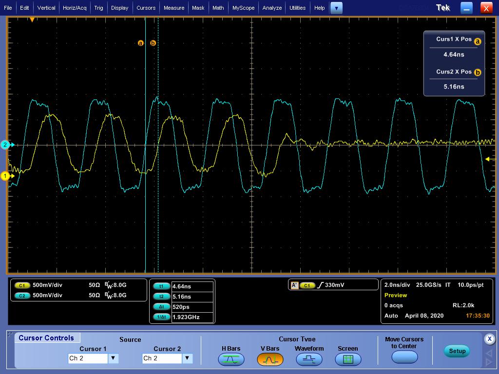
    I re-calculated EMIFs using latest app.note you mentioned, but they could not find any improvement when they checked it using oscilloscope with differential probe and they are doubting if it will be improved in the real test.

    May I ask your opinion if it is reasonable to understand there is no improvement based on oscilloscope measurement or should they do SI integrity test?

    As you see, the time interval between 'a' and 'b' is almost same - 520ps.

    1. Oscilloscope shot using differential probe with previous EMIFs

    2. Oscilloscope shot using differential probe with new EMIFs 

    I found exact their memory part name is 

    K4B1G1646I-BCNB

    The calculated new EMIF values using new  are

    Thanks and Best Regards,

    SI.

  • SI, it is the PHY registers that are important here.  Can you ensure that you are also using the updated PHY register settings in the code?

    If you look at the uboot tab in the spreadsheet, it will show which structures need to be updated based on the inputs to the spreadsheet.  Please post both the old and new structures so I can help compare.  And ensure the new structures are used in the call to config_ddr()

    REgards,

    James

  • Hi James,

    I found they did not applied PHY register settings and waiting their result again.

    In the meantime, I would like to check you can expect if there is any side effects for your code modification in the ddr.c file for 'Reset to CKE' time change.

    After this change in the ddr.c, they found the 'Reset to CKE' timing was changed to '532us' from '132us' in their oscilloscope shot.

    Their QA team now requested to check if there is side effect can be expected in this code change, and I think there should be no issue based on your explanation in the above, but I would like to check with you.

    Please let me know you opinion on this.

    Thanks and Best Regards,

    SI.

  • SI, there should be no side effect, this is just a one time setting to ensure the correct Reset to CKE timing.  They just need to make sure that during normal operation, the SDRAM_REF_CTRL = 0xC30.  Based on the code they showed, this should be the case, but they should double check. This will ensure the same operation as before the change.

    REgards,

    James

  • Hi James,

    Thanks for your response, and tDQSS timing issue was also resolved after applying new PHY values.

    BTW, Is this modification in ddr.c applied in the Linux SDK?

    I debugged below issue for other customer and resolved it after modifying  ddr.c as above.

    https://e2e.ti.com/support/processors/f/791/t/895362

    The situation was that memory access failed in the SPL although there is no issue to access using GEL file.

    The SPL was hang in the memcpy() function after ddr configuration done, but memory can be accessed after loading GEL file.

    After modifying in ddr.c file as you mentioned, the hang was removed in the SPL and there was no issue to access memory.

    Does this modification in ddr.c help to ensure the correct Reset to CKE timing in most DDR3 memories?

    if this modification in ddr.c is just to ensure the correct Reset to CKE timing without any side effect, I'm wondering why this modification will not be applied in the SDK.

    Their DDR3L memory is MT41K512M16VRN-107 IT:P..

    Thanks and Best Regards,

    SI.