This thread has been locked.

If you have a related question, please click the "Ask a related question" button in the top right corner. The newly created question will be automatically linked to this question.

TCIEVMK2X: BMC Power Issue: The signal SOC_POWER_GOOD has failed to assert

Part Number: TCIEVMK2X

Hello community,

We are using XTCIEVMK2X EVMs for our project. The version of the EVMs we use are v3.0. Accordingly, default BMC versions were 1.0.2.5 and UCD versions were 104_A02, 78_A02 and 52_A03.

We searched SOC_POWER_GOOD in Technical Documents and here in e2e.ti, It seems that some SOC_POWER_GOOD problems can be resolved with UCD Update. 

First of all, we tried UCD Update, But bmc_tool.py script always failed(i2c error). So we searched bmc_tool.py i2c error, It seems that some i2c errors can be resolved with BMC Update.

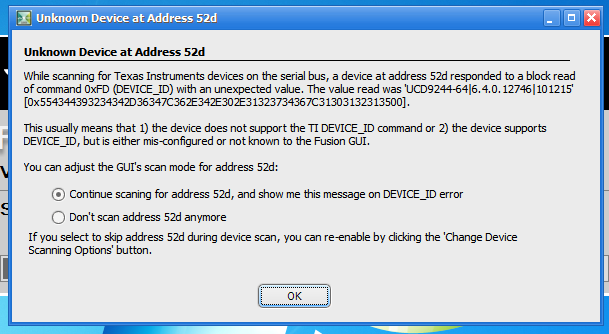
So, we tried BMC Update according to BMC_In-Field_Update, BMC has updated from 1.0.2.5 to 1.0.2.6. With 1.0.2.6 version BMCs, bmc_tool.py has succeed to update UCDs without error. But, when UCD versions have been got with bmc_tool.py, results seems corrupted like below. What is the reason for this corruption? If UCDs updates completed without error but with this corruption, can we say updates completed successfully?

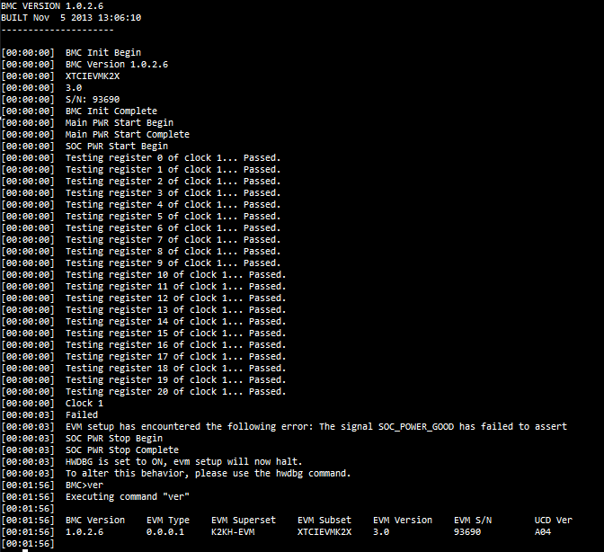
After updates, BMC outputs here;

1.0.2.6 version BMC firmware and 104_A02-78_A02-52_A03 versions UCD firmwares are the most current versions we can find. Is there any newer versions for any of them? 

We haven't been working for a while due to "SOC_POWER_GOOD " error on the cards. How can we overcome this problem?

Thank you,

Best Regards,

Srt

  • Hi community,

    Power problem still continues.

    We searched alternative ways to overcome Power issues when we can't get result with "bmc_tool.py". 

    First of all, we tried to reconfigure UCD Power chips with Fusion Digital Power Studio v3.0.42,  but Errors occured for all chips like this "Unknown Device at Address 52d&78d&104d".

    We tried Fusion Digital Power Designer v7.2.1(for an alternative to Fusion Digital Power Studio v3.0.42). With this program, There was no "Unknown Device" errors, unlike previous one. when we tried "Import to Device" options for all devices(52, 78, 104),  Only one of them completed without error(Only 104 successfully completed). "WRITE VERIFICATION READ BACK FAILED" errors occured for other two devices.

    Here is all outputs belongs to 3 Devices:

    Write Log:
    
    Turn all rails off via PAGE = 0xFF
    Starting write of 349 parameters ...
    Wrote VOUT_MODE [0x20,Rail #1] EXP -12 [0x14] to RAM
    Wrote VOUT_MODE [0x20,Rail #2] EXP -14 [0x12] to RAM
    Wrote VOUT_MODE [0x20,Rail #3] EXP -13 [0x13] to RAM
    Wrote VOUT_MODE [0x20,Rail #4] EXP -13 [0x13] to RAM
    Wrote VOUT_MODE [0x20,Rail #5] EXP -13 [0x13] to RAM
    Wrote VOUT_MODE [0x20,Rail #6] EXP -14 [0x12] to RAM
    Wrote VOUT_MODE [0x20,Rail #7] EXP -14 [0x12] to RAM
    Wrote VOUT_MODE [0x20,Rail #8] EXP -11 [0x15] to RAM
    Wrote VOUT_MODE [0x20,Rail #9] EXP -13 [0x13] to RAM
    Wrote VOUT_MODE [0x20,Rail #10] EXP 0 [0x00] to RAM
    Wrote MONITOR_CONFIG [MFR 05,0xD5] Pin 1 MON1: Rail #4, Type Voltage; Pin 2 MON2: Rail #5, Type Voltage; Pin 38 MON3: Rail #8, Type Voltage, HW Comparator, AVS); Pin 39 MON4: Rail #1, Type Voltage, HW Comparator, AVS); Pin 40 MON5: Rail #3, Type Voltage, HW Comparator, AVS); Pin 41 MON6: Rail #2, Type Voltage, HW Comparator, AVS); Pin 42 MON7: Rail #6, Type Voltage; Pin 45 MON8: Rail #7, Type Voltage; Pin 46 MON9: Rail #9, Type Voltage; Pin 48 MON10: Rail #10, Type Temperature; Pin 37 MON11: Not Assigned [0x2324878082812526284900] to RAM
    Wrote GPI_CONFIG [MFR 41,0xF9] Inputs: Pin 22 GPI1_PWM1 ActiveHigh Input,Pin 23 GPI2_PWM2 ActiveHigh Input [0x454D0000000000000000000000] to RAM
    Wrote SEQ_CONFIG [MFR 38,0xF6,Rail #1] Rail On Dep: <None> | GPI On Dep: S | Rail Off Dep: Rail #2 | GPI Off Dep: <None> | Fault Dep: <None> | Enable: Pin 7 GPIO4 ActiveHigh ActivelyDrivenOutput; Seq On Timeout: 0 / Wait Indefinitely; Seq Off Timeout: 0 / Wait Indefinitely [0x960100000000000000020000] to RAM
    Wrote SEQ_CONFIG [MFR 38,0xF6,Rail #2] Rail On Dep: Rail #1 | GPI On Dep: <None> | Rail Off Dep: Rail #3 | GPI Off Dep: <None> | Fault Dep: <None> | Enable: Pin 21 GPIO14 ActiveHigh ActivelyDrivenOutput; Seq On Timeout: 0 / Wait Indefinitely; Seq Off Timeout: 0 / Wait Indefinitely [0x560000000000000100040000] to RAM
    Wrote SEQ_CONFIG [MFR 38,0xF6,Rail #3] Rail On Dep: Rail #2 | GPI On Dep: <None> | Rail Off Dep: Rail #4 | GPI Off Dep: <None> | Fault Dep: <None> | Enable: Pin 18 GPIO13 ActiveHigh ActivelyDrivenOutput; Seq On Timeout: 0 / Wait Indefinitely; Seq Off Timeout: 0 / Wait Indefinitely [0x9E0000000000000200080000] to RAM
    Wrote SEQ_CONFIG [MFR 38,0xF6,Rail #4] Rail On Dep: <None> | GPI On Dep: T | Rail Off Dep: Rail #5 | GPI Off Dep: <None> | Fault Dep: <None> | Enable: Unassigned; Seq On Timeout: 0 / Wait Indefinitely; Seq Off Timeout: 0 / Wait Indefinitely [0x000200000000000000100000] to RAM
    Wrote SEQ_CONFIG [MFR 38,0xF6,Rail #5] Rail On Dep: Rail #4 | GPI On Dep: <None> | Rail Off Dep: Rail #6,7 | GPI Off Dep: <None> | Fault Dep: <None> | Enable: Unassigned; Seq On Timeout: 0 / Wait Indefinitely; Seq Off Timeout: 0 / Wait Indefinitely [0x000000000000000800600000] to RAM
    Wrote SEQ_CONFIG [MFR 38,0xF6,Rail #6] Rail On Dep: Rail #5 | GPI On Dep: <None> | Rail Off Dep: Rail #9 | GPI Off Dep: <None> | Fault Dep: <None> | Enable: Pin 26 GPIO17 ActiveHigh ActivelyDrivenOutput; Seq On Timeout: 0 / Wait Indefinitely; Seq Off Timeout: 0 / Wait Indefinitely [0xB60000000000001001000000] to RAM
    Wrote SEQ_CONFIG [MFR 38,0xF6,Rail #7] Rail On Dep: Rail #5 | GPI On Dep: <None> | Rail Off Dep: Rail #8 | GPI Off Dep: <None> | Fault Dep: <None> | Enable: Unassigned; Seq On Timeout: 0 / Wait Indefinitely; Seq Off Timeout: 0 / Wait Indefinitely [0x5C0000000000001000800000] to RAM
    Wrote SEQ_CONFIG [MFR 38,0xF6,Rail #8] Rail On Dep: Rail #6,7 | GPI On Dep: <None> | Rail Off Dep: Rail #9 | GPI Off Dep: <None> | Fault Dep: <None> | Enable: Pin 6 GPIO3 ActiveHigh ActivelyDrivenOutput; Seq On Timeout: 0 / Wait Indefinitely; Seq Off Timeout: 0 / Wait Indefinitely [0x8E0000000000006001000000] to RAM
    Wrote SEQ_CONFIG [MFR 38,0xF6,Rail #9] Rail On Dep: Rail #8 | GPI On Dep: <None> | Rail Off Dep: <None> | GPI Off Dep: <None> | Fault Dep: <None> | Enable: Unassigned; Seq On Timeout: 0 / Wait Indefinitely; Seq Off Timeout: 0 / Wait Indefinitely [0x040000000000008000000000] to RAM
    Wrote SEQ_CONFIG [MFR 38,0xF6,Rail #10] Rail On Dep: <None> | GPI On Dep: <None> | Rail Off Dep: <None> | GPI Off Dep: <None> | Fault Dep: <None> | Enable: Unassigned; Seq On Timeout: 0 / Wait Indefinitely; Seq Off Timeout: 0 / Wait Indefinitely [0x040000000000000000000000] to RAM
    Wrote GPO_CONFIG_1 [MFR 40,0xF8] Pin 4 GPIO1 ActiveHigh ActivelyDrivenOutput; INPUT_S � INPUT_T � RAIL2 � RAIL3 [POWER_GOOD] [0x7E0005000000060300000000000000000000000000] to RAM
    Wrote GPO_CONFIG_2 [MFR 40,0xF8] Pin 24 GPIO15 ActiveHigh ActivelyDrivenOutput; INPUT_S � RAIL2 � RAIL3 [POWER_GOOD] [0xA60005008000060100000000000000000000000000] to RAM
    Wrote GPO_CONFIG_3 [MFR 40,0xF8] Pin 5 GPIO2 ActiveHigh ActivelyDrivenOutput; INPUT_S � INPUT_T � OUTPUT_X � OUTPUT_X � RAIL2 � RAIL3 � RAIL4 [POWER_GOOD] [0x8600050000000E0303000000000000000000000000] to RAM
    Wrote GPO_CONFIG_4 [MFR 40,0xF8] Pin 25 GPIO16 ActiveHigh ActivelyDrivenOutput; INPUT_S � INPUT_T � OUTPUT_X � OUTPUT_X � OUTPUT_X � RAIL2 � RAIL3 � RAIL4 � RAIL5 � RAIL6 � RAIL7 [POWER_GOOD] [0xAE00050000007E0307000000000000000000000000] to RAM
    Wrote GPO_CONFIG_5 [MFR 40,0xF8] Unassigned; No Mask [0x000000000000000000000000000000000000000000] to RAM
    Wrote GPO_CONFIG_6 [MFR 40,0xF8] Unassigned; No Mask [0x000000000000000000000000000000000000000000] to RAM
    Wrote GPO_CONFIG_7 [MFR 40,0xF8] Unassigned; No Mask [0x000000000000000000000000000000000000000000] to RAM
    Wrote GPO_CONFIG_8 [MFR 40,0xF8] Unassigned; No Mask [0x000000000000000000000000000000000000000000] to RAM
    Wrote GPO_CONFIG_9 [MFR 40,0xF8] Unassigned; No Mask [0x000000000000000000000000000000000000000000] to RAM
    Wrote GPO_CONFIG_10 [MFR 40,0xF8] Unassigned; No Mask [0x000000000000000000000000000000000000000000] to RAM
    Wrote PWM_CONFIG_0 [MFR 17,0xE1] Pin_ID = 0; Duty Cycle: 0.0 %; Frequency: 0 Hz; Phase: 0.0 deg [0x8800000000008000] to RAM
    Wrote PWM_CONFIG_1 [MFR 17,0xE1] Pin_ID = 1; Duty Cycle: 0.0 %; Frequency: 0 Hz; Phase: 0.0 deg [0x8800000000008000] to RAM
    Wrote PWM_CONFIG_2 [MFR 17,0xE1] Pin_ID = 2; Duty Cycle: 0.0 %; Frequency: 0 Hz; Phase: 0.0 deg [0x8800000000008000] to RAM
    Wrote PWM_CONFIG_3 [MFR 17,0xE1] Pin_ID = 3; Duty Cycle: 0.0 %; Frequency: 0 Hz; Phase: 0.0 deg [0x8800000000008000] to RAM
    Wrote PWM_CONFIG_4 [MFR 17,0xE1] Pin_ID = 4; Duty Cycle: 90.0 %; Frequency: 15.26 kHz; Phase: 0.0 deg [0xEAD000003B9B8000] to RAM
    Wrote PWM_CONFIG_5 [MFR 17,0xE1] Pin_ID = 5; Duty Cycle: 0.0 %; Frequency: 0 Hz; Phase: 0.0 deg [0x8800000000008000] to RAM
    Wrote PWM_CONFIG_6 [MFR 17,0xE1] Pin_ID = 6; Duty Cycle: 0.0 %; Frequency: 0 Hz; Phase: 0.0 deg [0x8800000000008000] to RAM
    Wrote PWM_CONFIG_7 [MFR 17,0xE1] Pin_ID = 7; Duty Cycle: 0.0 %; Frequency: 0 Hz; Phase: 0.0 deg [0x8800000000008000] to RAM
    Wrote PWM_CONFIG_8 [MFR 17,0xE1] Pin_ID = 8; Duty Cycle: 0.0 %; Frequency: 0 Hz; Phase: 0.0 deg [0x8800000000000000] to RAM
    Wrote PWM_CONFIG_9 [MFR 17,0xE1] Pin_ID = 9; Duty Cycle: 0.0 %; Frequency: 0 Hz; Phase: 0.0 deg [0x8800000000000000] to RAM
    Wrote MARGIN_CONFIG [MFR 37,0xF5,Rail #1] Mode: Disabled; Increase Duty Cycle decreases Voltage; Ignore Faults: False; PWM Pin: ID 0, # 10 FPWM1_GPIO5 [0x00] to RAM
    Wrote MARGIN_CONFIG [MFR 37,0xF5,Rail #2] Mode: Disabled; Increase Duty Cycle decreases Voltage; Ignore Faults: False; PWM Pin: ID 0, # 10 FPWM1_GPIO5 [0x00] to RAM
    Wrote MARGIN_CONFIG [MFR 37,0xF5,Rail #3] Mode: Disabled; Increase Duty Cycle decreases Voltage; Ignore Faults: False; PWM Pin: ID 0, # 10 FPWM1_GPIO5 [0x00] to RAM
    Wrote MARGIN_CONFIG [MFR 37,0xF5,Rail #4] Mode: Disabled; Increase Duty Cycle decreases Voltage; Ignore Faults: False; PWM Pin: ID 0, # 10 FPWM1_GPIO5 [0x00] to RAM
    Wrote MARGIN_CONFIG [MFR 37,0xF5,Rail #5] Mode: Disabled; Increase Duty Cycle decreases Voltage; Ignore Faults: False; PWM Pin: ID 0, # 10 FPWM1_GPIO5 [0x00] to RAM
    Wrote MARGIN_CONFIG [MFR 37,0xF5,Rail #6] Mode: Disabled; Increase Duty Cycle decreases Voltage; Ignore Faults: False; PWM Pin: ID 0, # 10 FPWM1_GPIO5 [0x00] to RAM
    Wrote MARGIN_CONFIG [MFR 37,0xF5,Rail #7] Mode: Disabled; Increase Duty Cycle decreases Voltage; Ignore Faults: False; PWM Pin: ID 0, # 10 FPWM1_GPIO5 [0x00] to RAM
    Wrote MARGIN_CONFIG [MFR 37,0xF5,Rail #8] Mode: Disabled; Increase Duty Cycle decreases Voltage; Ignore Faults: False; PWM Pin: ID 0, # 10 FPWM1_GPIO5 [0x00] to RAM
    Wrote MARGIN_CONFIG [MFR 37,0xF5,Rail #9] Mode: Disabled; Increase Duty Cycle decreases Voltage; Ignore Faults: False; PWM Pin: ID 0, # 10 FPWM1_GPIO5 [0x00] to RAM
    Wrote MARGIN_CONFIG [MFR 37,0xF5,Rail #10] Mode: Disabled; Increase Duty Cycle decreases Voltage; Ignore Faults: False; PWM Pin: ID 0, # 10 FPWM1_GPIO5 [0x00] to RAM
    Wrote GPIO_CONFIG_0 [MFR 43,0xFB] Enable: False; Out_Enable: False; Out_Value: False; Status: False [0x00] to RAM
    Wrote GPIO_CONFIG_1 [MFR 43,0xFB] Enable: False; Out_Enable: False; Out_Value: False; Status: False [0x00] to RAM
    Wrote GPIO_CONFIG_2 [MFR 43,0xFB] Enable: False; Out_Enable: False; Out_Value: False; Status: False [0x00] to RAM
    Wrote GPIO_CONFIG_3 [MFR 43,0xFB] Enable: False; Out_Enable: False; Out_Value: False; Status: False [0x00] to RAM
    Wrote GPIO_CONFIG_4 [MFR 43,0xFB] Enable: False; Out_Enable: False; Out_Value: False; Status: True [0x08] to RAM
    Wrote GPIO_CONFIG_5 [MFR 43,0xFB] Enable: False; Out_Enable: False; Out_Value: False; Status: False [0x00] to RAM
    Wrote GPIO_CONFIG_6 [MFR 43,0xFB] Enable: False; Out_Enable: False; Out_Value: False; Status: False [0x00] to RAM
    Wrote GPIO_CONFIG_7 [MFR 43,0xFB] Enable: False; Out_Enable: False; Out_Value: False; Status: False [0x00] to RAM
    Wrote GPIO_CONFIG_8 [MFR 43,0xFB] Enable: False; Out_Enable: False; Out_Value: False; Status: True [0x08] to RAM
    Wrote GPIO_CONFIG_9 [MFR 43,0xFB] Enable: False; Out_Enable: False; Out_Value: False; Status: True [0x08] to RAM
    Wrote GPIO_CONFIG_10 [MFR 43,0xFB] Enable: False; Out_Enable: False; Out_Value: False; Status: True [0x08] to RAM
    Wrote GPIO_CONFIG_11 [MFR 43,0xFB] Enable: False; Out_Enable: False; Out_Value: False; Status: True [0x08] to RAM
    Wrote GPIO_CONFIG_12 [MFR 43,0xFB] Enable: False; Out_Enable: False; Out_Value: False; Status: True [0x08] to RAM
    Wrote GPIO_CONFIG_13 [MFR 43,0xFB] Enable: False; Out_Enable: False; Out_Value: False; Status: True [0x08] to RAM
    Wrote GPIO_CONFIG_14 [MFR 43,0xFB] Enable: False; Out_Enable: False; Out_Value: False; Status: True [0x08] to RAM
    Wrote GPIO_CONFIG_15 [MFR 43,0xFB] Enable: False; Out_Enable: False; Out_Value: False; Status: True [0x08] to RAM
    Wrote GPIO_CONFIG_16 [MFR 43,0xFB] Enable: False; Out_Enable: False; Out_Value: False; Status: True [0x08] to RAM
    Wrote GPIO_CONFIG_17 [MFR 43,0xFB] Enable: False; Out_Enable: False; Out_Value: False; Status: True [0x08] to RAM
    Wrote GPIO_CONFIG_18 [MFR 43,0xFB] Enable: False; Out_Enable: False; Out_Value: False; Status: True [0x08] to RAM
    Wrote GPIO_CONFIG_19 [MFR 43,0xFB] Enable: False; Out_Enable: False; Out_Value: False; Status: True [0x08] to RAM
    Wrote GPIO_CONFIG_20 [MFR 43,0xFB] Enable: False; Out_Enable: False; Out_Value: False; Status: True [0x08] to RAM
    Wrote GPIO_CONFIG_21 [MFR 43,0xFB] Enable: False; Out_Enable: False; Out_Value: False; Status: True [0x08] to RAM
    Wrote GPIO_CONFIG_22 [MFR 43,0xFB] Enable: False; Out_Enable: False; Out_Value: False; Status: True [0x08] to RAM
    Wrote LOGGED_FAULT_DETAIL_ENABLES [MFR 31,0xEF] Common: LOG_NOT_EMPTY,SYSTEM_WATCHDOG_TIMEOUT,RESEQUENCE_ERROR,WATCHDOG_TIMEOUT,RESERVED4,RESERVED5,RESERVED6,RESERVED7; GPI: #1,2,3,4,5,6,7,8; Rail #1: VOUT_OV,VOUT_UV,TON_MAX,IOUT_OC,IOUT_UC,TEMPERATURE_OT,SEQ_ON_TIMEOUT,SEQ_OFF_TIMEOUT; Rail #2: VOUT_OV,VOUT_UV,TON_MAX,IOUT_OC,IOUT_UC,TEMPERATURE_OT,SEQ_ON_TIMEOUT,SEQ_OFF_TIMEOUT; Rail #3: VOUT_OV,VOUT_UV,TON_MAX,IOUT_OC,IOUT_UC,TEMPERATURE_OT,SEQ_ON_TIMEOUT,SEQ_OFF_TIMEOUT; Rail #4: VOUT_OV,VOUT_UV,TON_MAX,IOUT_OC,IOUT_UC,TEMPERATURE_OT,SEQ_ON_TIMEOUT,SEQ_OFF_TIMEOUT; Rail #5: VOUT_OV,VOUT_UV,TON_MAX,IOUT_OC,IOUT_UC,TEMPERATURE_OT,SEQ_ON_TIMEOUT,SEQ_OFF_TIMEOUT; Rail #6: VOUT_OV,VOUT_UV,TON_MAX,IOUT_OC,IOUT_UC,TEMPERATURE_OT,SEQ_ON_TIMEOUT,SEQ_OFF_TIMEOUT; Rail #7: VOUT_OV,VOUT_UV,TON_MAX,IOUT_OC,IOUT_UC,TEMPERATURE_OT,SEQ_ON_TIMEOUT,SEQ_OFF_TIMEOUT; Rail #8: VOUT_OV,VOUT_UV,TON_MAX,IOUT_OC,IOUT_UC,TEMPERATURE_OT,SEQ_ON_TIMEOUT,SEQ_OFF_TIMEOUT; Rail #9: VOUT_OV,VOUT_UV,TON_MAX,IOUT_OC,IOUT_UC,TEMPERATURE_OT,SEQ_ON_TIMEOUT,SEQ_OFF_TIMEOUT; Rail #10: VOUT_OV,VOUT_UV,TON_MAX,IOUT_OC,IOUT_UC,TEMPERATURE_OT,SEQ_ON_TIMEOUT,SEQ_OFF_TIMEOUT [0xFFFFFFFFFFFFFFFFFFFFFFFF] to RAM
    Wrote MFR_DATE [0x9D] 130813 [0x313330383133] to RAM
    Wrote MFR_ID [0x99] MFR_ID [0x4D46525F4944] to RAM
    Wrote MFR_LOCATION [0x9C] TAIWAN [0x54414957414E] to RAM
    Wrote MFR_MODEL [0x9A] DSPM8305E [0x4453504D3833303545] to RAM
    Wrote MFR_REVISION [0x9B] 104_A04 [0x3130345F413034] to RAM
    Wrote MFR_SERIAL [0x9E] 000000 [0x303030303030] to RAM
    Wrote MISC_CONFIG [MFR 44,0xFC] Time Between Resequences: 0 msec; Resequence Abort: no; Max Resequences: 1; FIFO Mode: Disabled; Brownout Enable: no [0x0000] to RAM
    Wrote PIN_SELECTED_RAIL_STATES [MFR 13,0xDD] State 0: Enabled=No, Turn Off Mode=ImmediateOff, Rails States= Rail #1 Off, Rail #2 Off, Rail #3 Off, Rail #4 Off, Rail #5 Off, Rail #6 Off, Rail #7 Off, Rail #8 Off, Rail #9 Off, Rail #10 Off; State 1: Enabled=No, Turn Off Mode=ImmediateOff, Rails States= Rail #1 Off, Rail #2 Off, Rail #3 Off, Rail #4 Off, Rail #5 Off, Rail #6 Off, Rail #7 Off, Rail #8 Off, Rail #9 Off, Rail #10 Off; State 2: Enabled=No, Turn Off Mode=ImmediateOff, Rails States= Rail #1 Off, Rail #2 Off, Rail #3 Off, Rail #4 Off, Rail #5 Off, Rail #6 Off, Rail #7 Off, Rail #8 Off, Rail #9 Off, Rail #10 Off; State 3: Enabled=No, Turn Off Mode=ImmediateOff, Rails States= Rail #1 Off, Rail #2 Off, Rail #3 Off, Rail #4 Off, Rail #5 Off, Rail #6 Off, Rail #7 Off, Rail #8 Off, Rail #9 Off, Rail #10 Off; State 4: Enabled=No, Turn Off Mode=ImmediateOff, Rails States= Rail #1 Off, Rail #2 Off, Rail #3 Off, Rail #4 Off, Rail #5 Off, Rail #6 Off, Rail #7 Off, Rail #8 Off, Rail #9 Off, Rail #10 Off; State 5: Enabled=No, Turn Off Mode=ImmediateOff, Rails States= Rail #1 Off, Rail #2 Off, Rail #3 Off, Rail #4 Off, Rail #5 Off, Rail #6 Off, Rail #7 Off, Rail #8 Off, Rail #9 Off, Rail #10 Off; State 6: Enabled=No, Turn Off Mode=ImmediateOff, Rails States= Rail #1 Off, Rail #2 Off, Rail #3 Off, Rail #4 Off, Rail #5 Off, Rail #6 Off, Rail #7 Off, Rail #8 Off, Rail #9 Off, Rail #10 Off; State 7: Enabled=No, Turn Off Mode=ImmediateOff, Rails States= Rail #1 Off, Rail #2 Off, Rail #3 Off, Rail #4 Off, Rail #5 Off, Rail #6 Off, Rail #7 Off, Rail #8 Off, Rail #9 Off, Rail #10 Off [0x000000000000000000000000000000000000] to RAM
    Wrote RESET_COUNT [MFR 12,0xDC] 0  [0x0000] to RAM
    Wrote RUN_TIME_CLOCK_TRIM [MFR 08,0xD8] 0.00 % [0x8800] to RAM
    Wrote SECURITY_BIT_MASK [MFR 34,0xF2] No commands write protected [0x0000000000000000000000000000000000000000000000000000000000000000] to RAM
    Wrote SYSTEM_RESET_CONFIG [MFR 02,0xD2] Disabled [0x000000000000000000] to RAM
    Wrote SYSTEM_WATCHDOG_CONFIG [MFR 03,0xD3] Disabled [0x00000000] to RAM
    Wrote FAULT_RESPONSES [MFR 25,0xE9,Rail #1] Retry Time: 10 msec| Max Volt Glitch Time: 0.0 msec| Max Other Glitch Time: 0 msec| VOUT_OV: Resequence: Disabled; Glitch filter: Disabled; Response: Shut down immediately; Restart: Restart up to 1 times| VOUT_UV: Resequence: Disabled; Glitch filter: Disabled; Response: Shut down immediately; Restart: Restart up to 1 times| IOUT_OC: Resequence: Disabled; Glitch filter: Disabled; Response: Ignore; Restart: N/A| IOUT_UC: Resequence: Disabled; Glitch filter: Disabled; Response: Ignore; Restart: N/A| OT: Resequence: Disabled; Glitch filter: Disabled; Response: Ignore; Restart: N/A| TON_MAX: Resequence: Disabled; Glitch filter: Disabled; Response: Ignore; Restart: N/A [0x8181000000000A0000] to RAM
    Wrote IOUT_CAL_GAIN [0x38,Rail #1] 10.0 m? [0xD280] to RAM
    Wrote IOUT_CAL_OFFSET [0x39,Rail #1] 0.000000 A [0x8000] to RAM
    Wrote IOUT_OC_FAULT_LIMIT [0x46,Rail #1] 0.000 A [0x8000] to RAM
    Wrote IOUT_OC_WARN_LIMIT [0x4A,Rail #1] 0.000 A [0x8000] to RAM
    Wrote IOUT_UC_FAULT_LIMIT [0x4B,Rail #1] 0.000 A [0x8000] to RAM
    Wrote OT_FAULT_LIMIT [0x4F,Rail #1] 255 �C [0xF3FC] to RAM
    Wrote OT_WARN_LIMIT [0x51,Rail #1] 255 �C [0xF3FC] to RAM
    Wrote POWER_GOOD_OFF [0x5F,Rail #1] 2.805 V [0x2CE1] to RAM
    Wrote POWER_GOOD_ON [0x5E,Rail #1] 2.970 V [0x2F85] to RAM
    Wrote TEMPERATURE_CAL_GAIN [MFR 20,0xE4,Rail #1] 100.0 �C/V [0xEB20] to RAM
    Wrote TEMPERATURE_CAL_OFFSET [MFR 21,0xE5,Rail #1] 0.00 �C [0x8000] to RAM
    Wrote TOFF_DELAY [0x64,Rail #1] 5.0 ms [0xCA80] to RAM
    Wrote TOFF_MAX_WARN_LIMIT [0x66,Rail #1] <No Limit> [0x7FFF] to RAM
    Wrote TON_DELAY [0x60,Rail #1] 5.0 ms [0xCA80] to RAM
    Wrote TON_MAX_FAULT_LIMIT [0x62,Rail #1] <No Limit> [0x8000] to RAM
    Wrote VOUT_CAL_MONITOR [MFR 01,0xD1,Rail #1] 0.000 V [0x0000] to RAM
    Wrote VOUT_COMMAND [0x21,Rail #1] 3.300 V [0x34CC] to RAM
    Wrote VOUT_MARGIN_HIGH [0x25,Rail #1] 3.465 V [0x3770] to RAM
    Wrote VOUT_MARGIN_LOW [0x26,Rail #1] 3.135 V [0x3228] to RAM
    Wrote VOUT_OV_FAULT_LIMIT [0x40,Rail #1] 3.795 V [0x3CB8] to RAM
    Wrote VOUT_OV_WARN_LIMIT [0x42,Rail #1] 3.630 V [0x3A14] to RAM
    Wrote VOUT_SCALE_MONITOR [0x2A,Rail #1] 0.600  [0xB266] to RAM
    Wrote VOUT_UV_FAULT_LIMIT [0x44,Rail #1] 2.805 V [0x2CE1] to RAM
    Wrote VOUT_UV_WARN_LIMIT [0x43,Rail #1] 2.970 V [0x2F85] to RAM
    Wrote FAULT_RESPONSES [MFR 25,0xE9,Rail #2] Retry Time: 10 msec| Max Volt Glitch Time: 0.0 msec| Max Other Glitch Time: 0 msec| VOUT_OV: Resequence: Disabled; Glitch filter: Disabled; Response: Shut down immediately; Restart: Restart up to 1 times| VOUT_UV: Resequence: Disabled; Glitch filter: Disabled; Response: Shut down immediately; Restart: Restart up to 1 times| IOUT_OC: Resequence: Disabled; Glitch filter: Disabled; Response: Ignore; Restart: N/A| IOUT_UC: Resequence: Disabled; Glitch filter: Disabled; Response: Ignore; Restart: N/A| OT: Resequence: Disabled; Glitch filter: Disabled; Response: Ignore; Restart: N/A| TON_MAX: Resequence: Disabled; Glitch filter: Disabled; Response: Ignore; Restart: N/A [0x8181000000000A0000] to RAM
    Wrote IOUT_CAL_GAIN [0x38,Rail #2] 10.0 m? [0xD280] to RAM
    Wrote IOUT_CAL_OFFSET [0x39,Rail #2] 0.000000 A [0x8000] to RAM
    Wrote IOUT_OC_FAULT_LIMIT [0x46,Rail #2] 0.000 A [0x8000] to RAM
    Wrote IOUT_OC_WARN_LIMIT [0x4A,Rail #2] 0.000 A [0x8000] to RAM
    Wrote IOUT_UC_FAULT_LIMIT [0x4B,Rail #2] 0.000 A [0x8000] to RAM
    Wrote OT_FAULT_LIMIT [0x4F,Rail #2] 255 �C [0xF3FC] to RAM
    Wrote OT_WARN_LIMIT [0x51,Rail #2] 255 �C [0xF3FC] to RAM
    Wrote POWER_GOOD_OFF [0x5F,Rail #2] 1.020 V [0x4147] to RAM
    Wrote POWER_GOOD_ON [0x5E,Rail #2] 1.080 V [0x451E] to RAM
    Wrote TEMPERATURE_CAL_GAIN [MFR 20,0xE4,Rail #2] 100.0 �C/V [0xEB20] to RAM
    Wrote TEMPERATURE_CAL_OFFSET [MFR 21,0xE5,Rail #2] 0.00 �C [0x8000] to RAM
    Wrote TOFF_DELAY [0x64,Rail #2] 5.0 ms [0xCA80] to RAM
    Wrote TOFF_MAX_WARN_LIMIT [0x66,Rail #2] <No Limit> [0x7FFF] to RAM
    Wrote TON_DELAY [0x60,Rail #2] 5.0 ms [0xCA80] to RAM
    Wrote TON_MAX_FAULT_LIMIT [0x62,Rail #2] <No Limit> [0x8000] to RAM
    Wrote VOUT_CAL_MONITOR [MFR 01,0xD1,Rail #2] 0.000 V [0x0000] to RAM
    Wrote VOUT_COMMAND [0x21,Rail #2] 1.200 V [0x4CCC] to RAM
    Wrote VOUT_MARGIN_HIGH [0x25,Rail #2] 1.260 V [0x50A3] to RAM
    Wrote VOUT_MARGIN_LOW [0x26,Rail #2] 1.140 V [0x48F5] to RAM
    Wrote VOUT_OV_FAULT_LIMIT [0x40,Rail #2] 1.380 V [0x5851] to RAM
    Wrote VOUT_OV_WARN_LIMIT [0x42,Rail #2] 1.320 V [0x547A] to RAM
    Wrote VOUT_SCALE_MONITOR [0x2A,Rail #2] 1.000  [0xBA00] to RAM
    Wrote VOUT_UV_FAULT_LIMIT [0x44,Rail #2] 1.020 V [0x4147] to RAM
    Wrote VOUT_UV_WARN_LIMIT [0x43,Rail #2] 1.080 V [0x451E] to RAM
    Wrote FAULT_RESPONSES [MFR 25,0xE9,Rail #3] Retry Time: 10 msec| Max Volt Glitch Time: 0.0 msec| Max Other Glitch Time: 0 msec| VOUT_OV: Resequence: Disabled; Glitch filter: Disabled; Response: Shut down immediately; Restart: Restart up to 1 times| VOUT_UV: Resequence: Disabled; Glitch filter: Disabled; Response: Shut down immediately; Restart: Restart up to 1 times| IOUT_OC: Resequence: Disabled; Glitch filter: Disabled; Response: Ignore; Restart: N/A| IOUT_UC: Resequence: Disabled; Glitch filter: Disabled; Response: Ignore; Restart: N/A| OT: Resequence: Disabled; Glitch filter: Disabled; Response: Ignore; Restart: N/A| TON_MAX: Resequence: Disabled; Glitch filter: Disabled; Response: Ignore; Restart: N/A [0x8181000000000A0000] to RAM
    Wrote IOUT_CAL_GAIN [0x38,Rail #3] 10.0 m? [0xD280] to RAM
    Wrote IOUT_CAL_OFFSET [0x39,Rail #3] 0.000000 A [0x8000] to RAM
    Wrote IOUT_OC_FAULT_LIMIT [0x46,Rail #3] 0.000 A [0x8000] to RAM
    Wrote IOUT_OC_WARN_LIMIT [0x4A,Rail #3] 0.000 A [0x8000] to RAM
    Wrote IOUT_UC_FAULT_LIMIT [0x4B,Rail #3] 0.000 A [0x8000] to RAM
    Wrote OT_FAULT_LIMIT [0x4F,Rail #3] 255 �C [0xF3FC] to RAM
    Wrote OT_WARN_LIMIT [0x51,Rail #3] 255 �C [0xF3FC] to RAM
    Wrote POWER_GOOD_OFF [0x5F,Rail #3] 2.125 V [0x4400] to RAM
    Wrote POWER_GOOD_ON [0x5E,Rail #3] 2.250 V [0x4800] to RAM
    Wrote TEMPERATURE_CAL_GAIN [MFR 20,0xE4,Rail #3] 100.0 �C/V [0xEB20] to RAM
    Wrote TEMPERATURE_CAL_OFFSET [MFR 21,0xE5,Rail #3] 0.00 �C [0x8000] to RAM
    Wrote TOFF_DELAY [0x64,Rail #3] 20.0 ms [0xDA80] to RAM
    Wrote TOFF_MAX_WARN_LIMIT [0x66,Rail #3] <No Limit> [0x7FFF] to RAM
    Wrote TON_DELAY [0x60,Rail #3] 5.0 ms [0xCA80] to RAM
    Wrote TON_MAX_FAULT_LIMIT [0x62,Rail #3] <No Limit> [0x8000] to RAM
    Wrote VOUT_CAL_MONITOR [MFR 01,0xD1,Rail #3] 0.000 V [0x0000] to RAM
    Wrote VOUT_COMMAND [0x21,Rail #3] 2.500 V [0x5000] to RAM
    Wrote VOUT_MARGIN_HIGH [0x25,Rail #3] 2.625 V [0x5400] to RAM
    Wrote VOUT_MARGIN_LOW [0x26,Rail #3] 2.375 V [0x4C00] to RAM
    Wrote VOUT_OV_FAULT_LIMIT [0x40,Rail #3] 2.875 V [0x5C00] to RAM
    Wrote VOUT_OV_WARN_LIMIT [0x42,Rail #3] 2.750 V [0x5800] to RAM
    Wrote VOUT_SCALE_MONITOR [0x2A,Rail #3] 0.800  [0xB333] to RAM
    Wrote VOUT_UV_FAULT_LIMIT [0x44,Rail #3] 2.125 V [0x4400] to RAM
    Wrote VOUT_UV_WARN_LIMIT [0x43,Rail #3] 2.250 V [0x4800] to RAM
    Wrote FAULT_RESPONSES [MFR 25,0xE9,Rail #4] Retry Time: 10 msec| Max Volt Glitch Time: 0.0 msec| Max Other Glitch Time: 0 msec| VOUT_OV: Resequence: Disabled; Glitch filter: Disabled; Response: Shut down immediately; Restart: Restart up to 1 times| VOUT_UV: Resequence: Disabled; Glitch filter: Disabled; Response: Shut down immediately; Restart: Restart up to 1 times| IOUT_OC: Resequence: Disabled; Glitch filter: Disabled; Response: Ignore; Restart: N/A| IOUT_UC: Resequence: Disabled; Glitch filter: Disabled; Response: Ignore; Restart: N/A| OT: Resequence: Disabled; Glitch filter: Disabled; Response: Ignore; Restart: N/A| TON_MAX: Resequence: Disabled; Glitch filter: Disabled; Response: Ignore; Restart: N/A [0x8181000000000A0000] to RAM
    Wrote IOUT_CAL_GAIN [0x38,Rail #4] 10.0 m? [0xD280] to RAM
    Wrote IOUT_CAL_OFFSET [0x39,Rail #4] 0.000000 A [0x8000] to RAM
    Wrote IOUT_OC_FAULT_LIMIT [0x46,Rail #4] 0.000 A [0x8000] to RAM
    Wrote IOUT_OC_WARN_LIMIT [0x4A,Rail #4] 0.000 A [0x8000] to RAM
    Wrote IOUT_UC_FAULT_LIMIT [0x4B,Rail #4] 0.000 A [0x8000] to RAM
    Wrote OT_FAULT_LIMIT [0x4F,Rail #4] 255 �C [0xF3FC] to RAM
    Wrote OT_WARN_LIMIT [0x51,Rail #4] 255 �C [0xF3FC] to RAM
    Wrote POWER_GOOD_OFF [0x5F,Rail #4] 1.700 V [0x3666] to RAM
    Wrote POWER_GOOD_ON [0x5E,Rail #4] 1.800 V [0x3999] to RAM
    Wrote TEMPERATURE_CAL_GAIN [MFR 20,0xE4,Rail #4] 100.0 �C/V [0xEB20] to RAM
    Wrote TEMPERATURE_CAL_OFFSET [MFR 21,0xE5,Rail #4] 0.00 �C [0x8000] to RAM
    Wrote TOFF_DELAY [0x64,Rail #4] 20.0 ms [0xDA80] to RAM
    Wrote TOFF_MAX_WARN_LIMIT [0x66,Rail #4] <No Limit> [0x7FFF] to RAM
    Wrote TON_DELAY [0x60,Rail #4] 42.0 ms [0xE2A0] to RAM
    Wrote TON_MAX_FAULT_LIMIT [0x62,Rail #4] <No Limit> [0x8000] to RAM
    Wrote VOUT_CAL_MONITOR [MFR 01,0xD1,Rail #4] 0.000 V [0x0000] to RAM
    Wrote VOUT_COMMAND [0x21,Rail #4] 2.000 V [0x4000] to RAM
    Wrote VOUT_MARGIN_HIGH [0x25,Rail #4] 2.100 V [0x4333] to RAM
    Wrote VOUT_MARGIN_LOW [0x26,Rail #4] 1.900 V [0x3CCC] to RAM
    Wrote VOUT_OV_FAULT_LIMIT [0x40,Rail #4] 2.300 V [0x4999] to RAM
    Wrote VOUT_OV_WARN_LIMIT [0x42,Rail #4] 2.200 V [0x4666] to RAM
    Wrote VOUT_SCALE_MONITOR [0x2A,Rail #4] 1.000  [0xBA00] to RAM
    Wrote VOUT_UV_FAULT_LIMIT [0x44,Rail #4] 1.700 V [0x3666] to RAM
    Wrote VOUT_UV_WARN_LIMIT [0x43,Rail #4] 1.800 V [0x3999] to RAM
    Wrote FAULT_RESPONSES [MFR 25,0xE9,Rail #5] Retry Time: 10 msec| Max Volt Glitch Time: 0.0 msec| Max Other Glitch Time: 0 msec| VOUT_OV: Resequence: Disabled; Glitch filter: Disabled; Response: Shut down immediately; Restart: Restart up to 1 times| VOUT_UV: Resequence: Disabled; Glitch filter: Disabled; Response: Shut down immediately; Restart: Restart up to 1 times| IOUT_OC: Resequence: Disabled; Glitch filter: Disabled; Response: Ignore; Restart: N/A| IOUT_UC: Resequence: Disabled; Glitch filter: Disabled; Response: Ignore; Restart: N/A| OT: Resequence: Disabled; Glitch filter: Disabled; Response: Ignore; Restart: N/A| TON_MAX: Resequence: Disabled; Glitch filter: Disabled; Response: Ignore; Restart: N/A [0x8181000000000A0000] to RAM
    Wrote IOUT_CAL_GAIN [0x38,Rail #5] 10.0 m? [0xD280] to RAM
    Wrote IOUT_CAL_OFFSET [0x39,Rail #5] 0.000000 A [0x8000] to RAM
    Wrote IOUT_OC_FAULT_LIMIT [0x46,Rail #5] 0.000 A [0x8000] to RAM
    Wrote IOUT_OC_WARN_LIMIT [0x4A,Rail #5] 0.000 A [0x8000] to RAM
    Wrote IOUT_UC_FAULT_LIMIT [0x4B,Rail #5] 0.000 A [0x8000] to RAM
    Wrote OT_FAULT_LIMIT [0x4F,Rail #5] 255 �C [0xF3FC] to RAM
    Wrote OT_WARN_LIMIT [0x51,Rail #5] 255 �C [0xF3FC] to RAM
    Wrote POWER_GOOD_OFF [0x5F,Rail #5] 1.700 V [0x3666] to RAM
    Wrote POWER_GOOD_ON [0x5E,Rail #5] 1.800 V [0x3999] to RAM
    Wrote TEMPERATURE_CAL_GAIN [MFR 20,0xE4,Rail #5] 100.0 �C/V [0xEB20] to RAM
    Wrote TEMPERATURE_CAL_OFFSET [MFR 21,0xE5,Rail #5] 0.00 �C [0x8000] to RAM
    Wrote TOFF_DELAY [0x64,Rail #5] 5.0 ms [0xCA80] to RAM
    Wrote TOFF_MAX_WARN_LIMIT [0x66,Rail #5] <No Limit> [0x7FFF] to RAM
    Wrote TON_DELAY [0x60,Rail #5] 40.0 ms [0xE280] to RAM
    Wrote TON_MAX_FAULT_LIMIT [0x62,Rail #5] <No Limit> [0x8000] to RAM
    Wrote VOUT_CAL_MONITOR [MFR 01,0xD1,Rail #5] 0.000 V [0x0000] to RAM
    Wrote VOUT_COMMAND [0x21,Rail #5] 2.000 V [0x4000] to RAM
    Wrote VOUT_MARGIN_HIGH [0x25,Rail #5] 2.100 V [0x4333] to RAM
    Wrote VOUT_MARGIN_LOW [0x26,Rail #5] 1.900 V [0x3CCC] to RAM
    Wrote VOUT_OV_FAULT_LIMIT [0x40,Rail #5] 2.300 V [0x4999] to RAM
    Wrote VOUT_OV_WARN_LIMIT [0x42,Rail #5] 2.200 V [0x4666] to RAM
    Wrote VOUT_SCALE_MONITOR [0x2A,Rail #5] 1.000  [0xBA00] to RAM
    Wrote VOUT_UV_FAULT_LIMIT [0x44,Rail #5] 1.700 V [0x3666] to RAM
    Wrote VOUT_UV_WARN_LIMIT [0x43,Rail #5] 1.800 V [0x3999] to RAM
    Wrote FAULT_RESPONSES [MFR 25,0xE9,Rail #6] Retry Time: 10 msec| Max Volt Glitch Time: 0.0 msec| Max Other Glitch Time: 0 msec| VOUT_OV: Resequence: Disabled; Glitch filter: Disabled; Response: Shut down immediately; Restart: Restart up to 1 times| VOUT_UV: Resequence: Disabled; Glitch filter: Disabled; Response: Shut down immediately; Restart: Restart up to 1 times| IOUT_OC: Resequence: Disabled; Glitch filter: Disabled; Response: Ignore; Restart: N/A| IOUT_UC: Resequence: Disabled; Glitch filter: Disabled; Response: Ignore; Restart: N/A| OT: Resequence: Disabled; Glitch filter: Disabled; Response: Ignore; Restart: N/A| TON_MAX: Resequence: Disabled; Glitch filter: Disabled; Response: Ignore; Restart: N/A [0x8181000000000A0000] to RAM
    Wrote IOUT_CAL_GAIN [0x38,Rail #6] 10.0 m? [0xD280] to RAM
    Wrote IOUT_CAL_OFFSET [0x39,Rail #6] 0.000000 A [0x8000] to RAM
    Wrote IOUT_OC_FAULT_LIMIT [0x46,Rail #6] 0.000 A [0x8000] to RAM
    Wrote IOUT_OC_WARN_LIMIT [0x4A,Rail #6] 0.000 A [0x8000] to RAM
    Wrote IOUT_UC_FAULT_LIMIT [0x4B,Rail #6] 0.000 A [0x8000] to RAM
    Wrote OT_FAULT_LIMIT [0x4F,Rail #6] 255 �C [0xF3FC] to RAM
    Wrote OT_WARN_LIMIT [0x51,Rail #6] 255 �C [0xF3FC] to RAM
    Wrote POWER_GOOD_OFF [0x5F,Rail #6] 0.638 V [0x28D4] to RAM
    Wrote POWER_GOOD_ON [0x5E,Rail #6] 0.675 V [0x2B33] to RAM
    Wrote TEMPERATURE_CAL_GAIN [MFR 20,0xE4,Rail #6] 100.0 �C/V [0xEB20] to RAM
    Wrote TEMPERATURE_CAL_OFFSET [MFR 21,0xE5,Rail #6] 0.00 �C [0x8000] to RAM
    Wrote TOFF_DELAY [0x64,Rail #6] 5.0 ms [0xCA80] to RAM
    Wrote TOFF_MAX_WARN_LIMIT [0x66,Rail #6] <No Limit> [0x7FFF] to RAM
    Wrote TON_DELAY [0x60,Rail #6] 5.0 ms [0xCA80] to RAM
    Wrote TON_MAX_FAULT_LIMIT [0x62,Rail #6] <No Limit> [0x8000] to RAM
    Wrote VOUT_CAL_MONITOR [MFR 01,0xD1,Rail #6] 0.000 V [0x0000] to RAM
    Wrote VOUT_COMMAND [0x21,Rail #6] 0.750 V [0x3000] to RAM
    Wrote VOUT_MARGIN_HIGH [0x25,Rail #6] 0.788 V [0x326E] to RAM
    Wrote VOUT_MARGIN_LOW [0x26,Rail #6] 0.712 V [0x2D91] to RAM
    Wrote VOUT_OV_FAULT_LIMIT [0x40,Rail #6] 0.862 V [0x372B] to RAM
    Wrote VOUT_OV_WARN_LIMIT [0x42,Rail #6] 0.825 V [0x34CC] to RAM
    Wrote VOUT_SCALE_MONITOR [0x2A,Rail #6] 1.000  [0xBA00] to RAM
    Wrote VOUT_UV_FAULT_LIMIT [0x44,Rail #6] 0.638 V [0x28D4] to RAM
    Wrote VOUT_UV_WARN_LIMIT [0x43,Rail #6] 0.675 V [0x2B33] to RAM
    Wrote FAULT_RESPONSES [MFR 25,0xE9,Rail #7] Retry Time: 10 msec| Max Volt Glitch Time: 0.0 msec| Max Other Glitch Time: 0 msec| VOUT_OV: Resequence: Disabled; Glitch filter: Disabled; Response: Shut down immediately; Restart: Restart up to 1 times| VOUT_UV: Resequence: Disabled; Glitch filter: Disabled; Response: Shut down immediately; Restart: Restart up to 1 times| IOUT_OC: Resequence: Disabled; Glitch filter: Disabled; Response: Ignore; Restart: N/A| IOUT_UC: Resequence: Disabled; Glitch filter: Disabled; Response: Ignore; Restart: N/A| OT: Resequence: Disabled; Glitch filter: Disabled; Response: Ignore; Restart: N/A| TON_MAX: Resequence: Disabled; Glitch filter: Disabled; Response: Ignore; Restart: N/A [0x8181000000000A0000] to RAM
    Wrote IOUT_CAL_GAIN [0x38,Rail #7] 10.0 m? [0xD280] to RAM
    Wrote IOUT_CAL_OFFSET [0x39,Rail #7] 0.000000 A [0x8000] to RAM
    Wrote IOUT_OC_FAULT_LIMIT [0x46,Rail #7] 0.000 A [0x8000] to RAM
    Wrote IOUT_OC_WARN_LIMIT [0x4A,Rail #7] 0.000 A [0x8000] to RAM
    Wrote IOUT_UC_FAULT_LIMIT [0x4B,Rail #7] 0.000 A [0x8000] to RAM
    Wrote OT_FAULT_LIMIT [0x4F,Rail #7] 255 �C [0xF3FC] to RAM
    Wrote OT_WARN_LIMIT [0x51,Rail #7] 255 �C [0xF3FC] to RAM
    Wrote POWER_GOOD_OFF [0x5F,Rail #7] 0.638 V [0x28D4] to RAM
    Wrote POWER_GOOD_ON [0x5E,Rail #7] 0.675 V [0x2B33] to RAM
    Wrote TEMPERATURE_CAL_GAIN [MFR 20,0xE4,Rail #7] 100.0 �C/V [0xEB20] to RAM
    Wrote TEMPERATURE_CAL_OFFSET [MFR 21,0xE5,Rail #7] 0.00 �C [0x8000] to RAM
    Wrote TOFF_DELAY [0x64,Rail #7] 5.0 ms [0xCA80] to RAM
    Wrote TOFF_MAX_WARN_LIMIT [0x66,Rail #7] <No Limit> [0x7FFF] to RAM
    Wrote TON_DELAY [0x60,Rail #7] 5.0 ms [0xCA80] to RAM
    Wrote TON_MAX_FAULT_LIMIT [0x62,Rail #7] <No Limit> [0x8000] to RAM
    Wrote VOUT_CAL_MONITOR [MFR 01,0xD1,Rail #7] 0.000 V [0x0000] to RAM
    Wrote VOUT_COMMAND [0x21,Rail #7] 0.750 V [0x3000] to RAM
    Wrote VOUT_MARGIN_HIGH [0x25,Rail #7] 0.788 V [0x326E] to RAM
    Wrote VOUT_MARGIN_LOW [0x26,Rail #7] 0.712 V [0x2D91] to RAM
    Wrote VOUT_OV_FAULT_LIMIT [0x40,Rail #7] 0.862 V [0x372B] to RAM
    Wrote VOUT_OV_WARN_LIMIT [0x42,Rail #7] 0.825 V [0x34CC] to RAM
    Wrote VOUT_SCALE_MONITOR [0x2A,Rail #7] 1.000  [0xBA00] to RAM
    Wrote VOUT_UV_FAULT_LIMIT [0x44,Rail #7] 0.638 V [0x28D4] to RAM
    Wrote VOUT_UV_WARN_LIMIT [0x43,Rail #7] 0.675 V [0x2B33] to RAM
    Wrote FAULT_RESPONSES [MFR 25,0xE9,Rail #8] Retry Time: 10 msec| Max Volt Glitch Time: 0.0 msec| Max Other Glitch Time: 0 msec| VOUT_OV: Resequence: Disabled; Glitch filter: Disabled; Response: Shut down immediately; Restart: Restart up to 1 times| VOUT_UV: Resequence: Disabled; Glitch filter: Disabled; Response: Shut down immediately; Restart: Restart up to 1 times| IOUT_OC: Resequence: Disabled; Glitch filter: Disabled; Response: Ignore; Restart: N/A| IOUT_UC: Resequence: Disabled; Glitch filter: Disabled; Response: Ignore; Restart: N/A| OT: Resequence: Disabled; Glitch filter: Disabled; Response: Ignore; Restart: N/A| TON_MAX: Resequence: Disabled; Glitch filter: Disabled; Response: Ignore; Restart: N/A [0x8181000000000A0000] to RAM
    Wrote IOUT_CAL_GAIN [0x38,Rail #8] 10.0 m? [0xD280] to RAM
    Wrote IOUT_CAL_OFFSET [0x39,Rail #8] 0.000000 A [0x8000] to RAM
    Wrote IOUT_OC_FAULT_LIMIT [0x46,Rail #8] 0.000 A [0x8000] to RAM
    Wrote IOUT_OC_WARN_LIMIT [0x4A,Rail #8] 0.000 A [0x8000] to RAM
    Wrote IOUT_UC_FAULT_LIMIT [0x4B,Rail #8] 0.000 A [0x8000] to RAM
    Wrote OT_FAULT_LIMIT [0x4F,Rail #8] 255 �C [0xF3FC] to RAM
    Wrote OT_WARN_LIMIT [0x51,Rail #8] 255 �C [0xF3FC] to RAM
    Wrote POWER_GOOD_OFF [0x5F,Rail #8] 4.250 V [0x2200] to RAM
    Wrote POWER_GOOD_ON [0x5E,Rail #8] 4.500 V [0x2400] to RAM
    Wrote TEMPERATURE_CAL_GAIN [MFR 20,0xE4,Rail #8] 100.0 �C/V [0xEB20] to RAM
    Wrote TEMPERATURE_CAL_OFFSET [MFR 21,0xE5,Rail #8] 0.00 �C [0x8000] to RAM
    Wrote TOFF_DELAY [0x64,Rail #8] 5.0 ms [0xCA80] to RAM
    Wrote TOFF_MAX_WARN_LIMIT [0x66,Rail #8] <No Limit> [0x7FFF] to RAM
    Wrote TON_DELAY [0x60,Rail #8] 5.0 ms [0xCA80] to RAM
    Wrote TON_MAX_FAULT_LIMIT [0x62,Rail #8] <No Limit> [0x8000] to RAM
    Wrote VOUT_CAL_MONITOR [MFR 01,0xD1,Rail #8] 0.000 V [0x0000] to RAM
    Wrote VOUT_COMMAND [0x21,Rail #8] 5.000 V [0x2800] to RAM
    Wrote VOUT_MARGIN_HIGH [0x25,Rail #8] 5.250 V [0x2A00] to RAM
    Wrote VOUT_MARGIN_LOW [0x26,Rail #8] 4.750 V [0x2600] to RAM
    Wrote VOUT_OV_FAULT_LIMIT [0x40,Rail #8] 6.500 V [0x3400] to RAM
    Wrote VOUT_OV_WARN_LIMIT [0x42,Rail #8] 5.500 V [0x2C00] to RAM
    Wrote VOUT_SCALE_MONITOR [0x2A,Rail #8] 0.400  [0xAB33] to RAM
    Wrote VOUT_UV_FAULT_LIMIT [0x44,Rail #8] 3.500 V [0x1C00] to RAM
    Wrote VOUT_UV_WARN_LIMIT [0x43,Rail #8] 4.500 V [0x2400] to RAM
    Wrote FAULT_RESPONSES [MFR 25,0xE9,Rail #9] Retry Time: 10 msec| Max Volt Glitch Time: 0.0 msec| Max Other Glitch Time: 0 msec| VOUT_OV: Resequence: Disabled; Glitch filter: Disabled; Response: Shut down immediately; Restart: Restart up to 1 times| VOUT_UV: Resequence: Disabled; Glitch filter: Disabled; Response: Shut down immediately; Restart: Restart up to 1 times| IOUT_OC: Resequence: Disabled; Glitch filter: Disabled; Response: Ignore; Restart: N/A| IOUT_UC: Resequence: Disabled; Glitch filter: Disabled; Response: Ignore; Restart: N/A| OT: Resequence: Disabled; Glitch filter: Disabled; Response: Ignore; Restart: N/A| TON_MAX: Resequence: Disabled; Glitch filter: Disabled; Response: Ignore; Restart: N/A [0x8181000000000A0000] to RAM
    Wrote IOUT_CAL_GAIN [0x38,Rail #9] 10.0 m? [0xD280] to RAM
    Wrote IOUT_CAL_OFFSET [0x39,Rail #9] 0.000000 A [0x8000] to RAM
    Wrote IOUT_OC_FAULT_LIMIT [0x46,Rail #9] 0.000 A [0x8000] to RAM
    Wrote IOUT_OC_WARN_LIMIT [0x4A,Rail #9] 0.000 A [0x8000] to RAM
    Wrote IOUT_UC_FAULT_LIMIT [0x4B,Rail #9] 0.000 A [0x8000] to RAM
    Wrote OT_FAULT_LIMIT [0x4F,Rail #9] 255 �C [0xF3FC] to RAM
    Wrote OT_WARN_LIMIT [0x51,Rail #9] 255 �C [0xF3FC] to RAM
    Wrote POWER_GOOD_OFF [0x5F,Rail #9] 1.530 V [0x30F5] to RAM
    Wrote POWER_GOOD_ON [0x5E,Rail #9] 1.620 V [0x33D7] to RAM
    Wrote TEMPERATURE_CAL_GAIN [MFR 20,0xE4,Rail #9] 100.0 �C/V [0xEB20] to RAM
    Wrote TEMPERATURE_CAL_OFFSET [MFR 21,0xE5,Rail #9] 0.00 �C [0x8000] to RAM
    Wrote TOFF_DELAY [0x64,Rail #9] 0.0 ms [0x8000] to RAM
    Wrote TOFF_MAX_WARN_LIMIT [0x66,Rail #9] <No Limit> [0x7FFF] to RAM
    Wrote TON_DELAY [0x60,Rail #9] 37.0 ms [0xE250] to RAM
    Wrote TON_MAX_FAULT_LIMIT [0x62,Rail #9] <No Limit> [0x8000] to RAM
    Wrote VOUT_CAL_MONITOR [MFR 01,0xD1,Rail #9] 0.000 V [0x0000] to RAM
    Wrote VOUT_COMMAND [0x21,Rail #9] 1.800 V [0x3999] to RAM
    Wrote VOUT_MARGIN_HIGH [0x25,Rail #9] 1.890 V [0x3C7A] to RAM
    Wrote VOUT_MARGIN_LOW [0x26,Rail #9] 1.710 V [0x36B8] to RAM
    Wrote VOUT_OV_FAULT_LIMIT [0x40,Rail #9] 2.070 V [0x423D] to RAM
    Wrote VOUT_OV_WARN_LIMIT [0x42,Rail #9] 1.980 V [0x3F5C] to RAM
    Wrote VOUT_SCALE_MONITOR [0x2A,Rail #9] 1.000  [0xBA00] to RAM
    Wrote VOUT_UV_FAULT_LIMIT [0x44,Rail #9] 1.530 V [0x30F5] to RAM
    Wrote VOUT_UV_WARN_LIMIT [0x43,Rail #9] 1.620 V [0x33D7] to RAM
    Wrote FAULT_RESPONSES [MFR 25,0xE9,Rail #10] Retry Time: 0 msec| Max Volt Glitch Time: 0.0 msec| Max Other Glitch Time: 0 msec| VOUT_OV: Resequence: Disabled; Glitch filter: Disabled; Response: Ignore; Restart: N/A| VOUT_UV: Resequence: Disabled; Glitch filter: Disabled; Response: Ignore; Restart: N/A| IOUT_OC: Resequence: Disabled; Glitch filter: Disabled; Response: Ignore; Restart: N/A| IOUT_UC: Resequence: Disabled; Glitch filter: Disabled; Response: Ignore; Restart: N/A| OT: Resequence: Disabled; Glitch filter: Disabled; Response: Ignore; Restart: N/A| TON_MAX: Resequence: Disabled; Glitch filter: Disabled; Response: Ignore; Restart: N/A [0x000000000000000000] to RAM
    Wrote IOUT_CAL_GAIN [0x38,Rail #10] 10.0 m? [0xD280] to RAM
    Wrote IOUT_CAL_OFFSET [0x39,Rail #10] 0.000000 A [0x8000] to RAM
    Wrote IOUT_OC_FAULT_LIMIT [0x46,Rail #10] 0.000 A [0x8000] to RAM
    Wrote IOUT_OC_WARN_LIMIT [0x4A,Rail #10] 0.000 A [0x8000] to RAM
    Wrote IOUT_UC_FAULT_LIMIT [0x4B,Rail #10] 0.000 A [0x8000] to RAM
    Wrote OT_FAULT_LIMIT [0x4F,Rail #10] 60 �C [0xE3C0] to RAM
    Wrote OT_WARN_LIMIT [0x51,Rail #10] 50 �C [0xE320] to RAM
    Wrote POWER_GOOD_OFF [0x5F,Rail #10] 0.000 V [0x0000] to RAM
    Wrote POWER_GOOD_ON [0x5E,Rail #10] 0.000 V [0x0000] to RAM
    Wrote TEMPERATURE_CAL_GAIN [MFR 20,0xE4,Rail #10] 50.0 �C/V [0xE320] to RAM
    Wrote TEMPERATURE_CAL_OFFSET [MFR 21,0xE5,Rail #10] 0.00 �C [0x8000] to RAM
    Wrote TOFF_DELAY [0x64,Rail #10] 0.0 ms [0x8000] to RAM
    Wrote TOFF_MAX_WARN_LIMIT [0x66,Rail #10] <No Limit> [0x7FFF] to RAM
    Wrote TON_DELAY [0x60,Rail #10] 0.0 ms [0x8000] to RAM
    Wrote TON_MAX_FAULT_LIMIT [0x62,Rail #10] <No Limit> [0x8000] to RAM
    Wrote VOUT_CAL_MONITOR [MFR 01,0xD1,Rail #10] 0.000 V [0x0000] to RAM
    Wrote VOUT_COMMAND [0x21,Rail #10] 0.000 V [0x0000] to RAM
    Wrote VOUT_MARGIN_HIGH [0x25,Rail #10] 0.000 V [0x0000] to RAM
    Wrote VOUT_MARGIN_LOW [0x26,Rail #10] 0.000 V [0x0000] to RAM
    Wrote VOUT_OV_FAULT_LIMIT [0x40,Rail #10] 0.000 V [0x0000] to RAM
    Wrote VOUT_OV_WARN_LIMIT [0x42,Rail #10] 0.000 V [0x0000] to RAM
    Wrote VOUT_SCALE_MONITOR [0x2A,Rail #10] 1.000  [0xBA00] to RAM
    Wrote VOUT_UV_FAULT_LIMIT [0x44,Rail #10] 0.000 V [0x0000] to RAM
    Wrote VOUT_UV_WARN_LIMIT [0x43,Rail #10] 0.000 V [0x0000] to RAM
    Wrote ON_OFF_CONFIG [0x02,Rail #1] Mode: Always Converting [0x02] to RAM
    Wrote ON_OFF_CONFIG [0x02,Rail #2] Mode: Always Converting [0x02] to RAM
    Wrote ON_OFF_CONFIG [0x02,Rail #3] Mode: Always Converting [0x02] to RAM
    Wrote ON_OFF_CONFIG [0x02,Rail #4] Mode: Always Converting [0x00] to RAM
    Wrote ON_OFF_CONFIG [0x02,Rail #5] Mode: Always Converting [0x00] to RAM
    Wrote ON_OFF_CONFIG [0x02,Rail #6] Mode: Always Converting [0x00] to RAM
    Wrote ON_OFF_CONFIG [0x02,Rail #7] Mode: Always Converting [0x00] to RAM
    Wrote ON_OFF_CONFIG [0x02,Rail #8] Mode: Always Converting [0x00] to RAM
    Wrote ON_OFF_CONFIG [0x02,Rail #9] Mode: Always Converting [0x00] to RAM
    Wrote ON_OFF_CONFIG [0x02,Rail #10] Mode: Always Converting [0x00] to RAM
    Wait minimum of 1000 ms before executing Store_Default...
    Pausing 1,000.00 ms
    Saving device configuration (RAM) to flash memory ...
    Pausing 1,500.00 ms for STORE_DEFAULT_ALL hold time
    STORE_DEFAULT complete with success; 1513 msec elapsed (max wait time = 2000 ms)
    STORE_DEFAULT is completed in 1513 ms, less than max wait time 2000 ms.
    Clearing data flash logs ...
    Pausing 1,000.00 ms for LOGGED_PAGE_PEAKS flash write
    Pausing 1,000.00 ms for LOGGED_PAGE_PEAKS flash write
    Pausing 1,000.00 ms for LOGGED_PAGE_PEAKS flash write
    Pausing 1,000.00 ms for LOGGED_PAGE_PEAKS flash write
    Pausing 1,000.00 ms for LOGGED_PAGE_PEAKS flash write
    Pausing 1,000.00 ms for LOGGED_PAGE_PEAKS flash write
    Pausing 1,000.00 ms for LOGGED_PAGE_PEAKS flash write
    Pausing 1,000.00 ms for LOGGED_PAGE_PEAKS flash write
    Pausing 1,000.00 ms for LOGGED_PAGE_PEAKS flash write
    Pausing 1,000.00 ms for LOGGED_PAGE_PEAKS flash write
    Pausing 1,000.00 ms for LOGGED_COMMON_PEAKS flash write
    Pausing 1,000.00 ms for LOGGED_FAULTS flash write
    Done!
    
    Error Log:


    Message
    IOUT_OC_FAULT_LIMIT [0x46,Rail #1]: the current encoded and the import encoded values are the same (0x0xCBE6) but the decoded values are different (7.797 vs 7.8). It might due to rounding, raw data is decoded differently in different firmwares, decoded depends on other register values, or else. The import encoded value (0x0xCBE6) will NOT be imported.
    IOUT_OC_WARN_LIMIT [0x4A,Rail #1]: the current encoded and the import encoded values are the same (0x0xCB26) but the decoded values are different (6.297 vs 6.3). It might due to rounding, raw data is decoded differently in different firmwares, decoded depends on other register values, or else. The import encoded value (0x0xCB26) will NOT be imported.
    IOUT_UC_FAULT_LIMIT [0x4B,Rail #1]: the current encoded and the import encoded values are the same (0x0xBC08) but the decoded values are different (-1.984 vs -1.98). It might due to rounding, raw data is decoded differently in different firmwares, decoded depends on other register values, or else. The import encoded value (0x0xBC08) will NOT be imported.
    SMBALERT_MASK_CML [0x1B,Rail #1]: unable to read the current value from the device: USB ADAPTER FIRMWARE DOES NOT SUPPORT PROCESS CALL TRANSACTIONS USED BY THIS COMMAND; CONTACT TI
    SMBALERT_MASK_INPUT [0x1B,Rail #1]: unable to read the current value from the device: USB ADAPTER FIRMWARE DOES NOT SUPPORT PROCESS CALL TRANSACTIONS USED BY THIS COMMAND; CONTACT TI
    SMBALERT_MASK_IOUT [0x1B,Rail #1]: unable to read the current value from the device: USB ADAPTER FIRMWARE DOES NOT SUPPORT PROCESS CALL TRANSACTIONS USED BY THIS COMMAND; CONTACT TI
    SMBALERT_MASK_MFR_SPECIFIC [0x1B,Rail #1]: unable to read the current value from the device: USB ADAPTER FIRMWARE DOES NOT SUPPORT PROCESS CALL TRANSACTIONS USED BY THIS COMMAND; CONTACT TI
    SMBALERT_MASK_OTHER [0x1B,Rail #1]: unable to read the current value from the device: USB ADAPTER FIRMWARE DOES NOT SUPPORT PROCESS CALL TRANSACTIONS USED BY THIS COMMAND; CONTACT TI
    SMBALERT_MASK_TEMPERATURE [0x1B,Rail #1]: unable to read the current value from the device: USB ADAPTER FIRMWARE DOES NOT SUPPORT PROCESS CALL TRANSACTIONS USED BY THIS COMMAND; CONTACT TI
    SMBALERT_MASK_VOUT [0x1B,Rail #1]: unable to read the current value from the device: USB ADAPTER FIRMWARE DOES NOT SUPPORT PROCESS CALL TRANSACTIONS USED BY THIS COMMAND; CONTACT TI
    IOUT_OC_WARN_LIMIT [0x4A,Rail #2]: the current encoded and the import encoded values are the same (0x0xD348) but the decoded values are different (13.125 vs 13.13). It might due to rounding, raw data is decoded differently in different firmwares, decoded depends on other register values, or else. The import encoded value (0x0xD348) will NOT be imported.
    IOUT_UC_FAULT_LIMIT [0x4B,Rail #2]: the current encoded and the import encoded values are the same (0x0xCDF0) but the decoded values are different (-4.125 vs -4.13). It might due to rounding, raw data is decoded differently in different firmwares, decoded depends on other register values, or else. The import encoded value (0x0xCDF0) will NOT be imported.
    SMBALERT_MASK_CML [0x1B,Rail #2]: unable to read the current value from the device: USB ADAPTER FIRMWARE DOES NOT SUPPORT PROCESS CALL TRANSACTIONS USED BY THIS COMMAND; CONTACT TI
    SMBALERT_MASK_INPUT [0x1B,Rail #2]: unable to read the current value from the device: USB ADAPTER FIRMWARE DOES NOT SUPPORT PROCESS CALL TRANSACTIONS USED BY THIS COMMAND; CONTACT TI
    SMBALERT_MASK_IOUT [0x1B,Rail #2]: unable to read the current value from the device: USB ADAPTER FIRMWARE DOES NOT SUPPORT PROCESS CALL TRANSACTIONS USED BY THIS COMMAND; CONTACT TI
    SMBALERT_MASK_MFR_SPECIFIC [0x1B,Rail #2]: unable to read the current value from the device: USB ADAPTER FIRMWARE DOES NOT SUPPORT PROCESS CALL TRANSACTIONS USED BY THIS COMMAND; CONTACT TI
    SMBALERT_MASK_OTHER [0x1B,Rail #2]: unable to read the current value from the device: USB ADAPTER FIRMWARE DOES NOT SUPPORT PROCESS CALL TRANSACTIONS USED BY THIS COMMAND; CONTACT TI
    SMBALERT_MASK_TEMPERATURE [0x1B,Rail #2]: unable to read the current value from the device: USB ADAPTER FIRMWARE DOES NOT SUPPORT PROCESS CALL TRANSACTIONS USED BY THIS COMMAND; CONTACT TI
    SMBALERT_MASK_VOUT [0x1B,Rail #2]: unable to read the current value from the device: USB ADAPTER FIRMWARE DOES NOT SUPPORT PROCESS CALL TRANSACTIONS USED BY THIS COMMAND; CONTACT TI
    IOUT_OC_FAULT_LIMIT [0x46,Rail #3]: the current encoded and the import encoded values are the same (0x0xCB1A) but the decoded values are different (6.203 vs 6.2). It might due to rounding, raw data is decoded differently in different firmwares, decoded depends on other register values, or else. The import encoded value (0x0xCB1A) will NOT be imported.
    IOUT_OC_WARN_LIMIT [0x4A,Rail #3]: the current encoded and the import encoded values are the same (0x0xCA9A) but the decoded values are different (5.203 vs 5.2). It might due to rounding, raw data is decoded differently in different firmwares, decoded depends on other register values, or else. The import encoded value (0x0xCA9A) will NOT be imported.
    IOUT_UC_FAULT_LIMIT [0x4B,Rail #3]: the current encoded and the import encoded values are the same (0x0xBD60) but the decoded values are different (-1.313 vs -1.31). It might due to rounding, raw data is decoded differently in different firmwares, decoded depends on other register values, or else. The import encoded value (0x0xBD60) will NOT be imported.
    SMBALERT_MASK_CML [0x1B,Rail #3]: unable to read the current value from the device: USB ADAPTER FIRMWARE DOES NOT SUPPORT PROCESS CALL TRANSACTIONS USED BY THIS COMMAND; CONTACT TI
    SMBALERT_MASK_INPUT [0x1B,Rail #3]: unable to read the current value from the device: USB ADAPTER FIRMWARE DOES NOT SUPPORT PROCESS CALL TRANSACTIONS USED BY THIS COMMAND; CONTACT TI
    SMBALERT_MASK_IOUT [0x1B,Rail #3]: unable to read the current value from the device: USB ADAPTER FIRMWARE DOES NOT SUPPORT PROCESS CALL TRANSACTIONS USED BY THIS COMMAND; CONTACT TI
    SMBALERT_MASK_MFR_SPECIFIC [0x1B,Rail #3]: unable to read the current value from the device: USB ADAPTER FIRMWARE DOES NOT SUPPORT PROCESS CALL TRANSACTIONS USED BY THIS COMMAND; CONTACT TI
    SMBALERT_MASK_OTHER [0x1B,Rail #3]: unable to read the current value from the device: USB ADAPTER FIRMWARE DOES NOT SUPPORT PROCESS CALL TRANSACTIONS USED BY THIS COMMAND; CONTACT TI
    SMBALERT_MASK_TEMPERATURE [0x1B,Rail #3]: unable to read the current value from the device: USB ADAPTER FIRMWARE DOES NOT SUPPORT PROCESS CALL TRANSACTIONS USED BY THIS COMMAND; CONTACT TI
    SMBALERT_MASK_VOUT [0x1B,Rail #3]: unable to read the current value from the device: USB ADAPTER FIRMWARE DOES NOT SUPPORT PROCESS CALL TRANSACTIONS USED BY THIS COMMAND; CONTACT TI
    IOUT_OC_FAULT_LIMIT [0x46,Rail #4]: the current encoded and the import encoded values are the same (0x0xD29A) but the decoded values are different (10.406 vs 10.41). It might due to rounding, raw data is decoded differently in different firmwares, decoded depends on other register values, or else. The import encoded value (0x0xD29A) will NOT be imported.
    IOUT_OC_WARN_LIMIT [0x4A,Rail #4]: the current encoded and the import encoded values are the same (0x0xD21A) but the decoded values are different (8.406 vs 8.41). It might due to rounding, raw data is decoded differently in different firmwares, decoded depends on other register values, or else. The import encoded value (0x0xD21A) will NOT be imported.
    IOUT_UC_FAULT_LIMIT [0x4B,Rail #4]: the current encoded and the import encoded values are the same (0x0xC55C) but the decoded values are different (-2.641 vs -2.64). It might due to rounding, raw data is decoded differently in different firmwares, decoded depends on other register values, or else. The import encoded value (0x0xC55C) will NOT be imported.
    SMBALERT_MASK_CML [0x1B,Rail #4]: unable to read the current value from the device: USB ADAPTER FIRMWARE DOES NOT SUPPORT PROCESS CALL TRANSACTIONS USED BY THIS COMMAND; CONTACT TI
    SMBALERT_MASK_INPUT [0x1B,Rail #4]: unable to read the current value from the device: USB ADAPTER FIRMWARE DOES NOT SUPPORT PROCESS CALL TRANSACTIONS USED BY THIS COMMAND; CONTACT TI
    SMBALERT_MASK_IOUT [0x1B,Rail #4]: unable to read the current value from the device: USB ADAPTER FIRMWARE DOES NOT SUPPORT PROCESS CALL TRANSACTIONS USED BY THIS COMMAND; CONTACT TI
    SMBALERT_MASK_MFR_SPECIFIC [0x1B,Rail #4]: unable to read the current value from the device: USB ADAPTER FIRMWARE DOES NOT SUPPORT PROCESS CALL TRANSACTIONS USED BY THIS COMMAND; CONTACT TI
    SMBALERT_MASK_OTHER [0x1B,Rail #4]: unable to read the current value from the device: USB ADAPTER FIRMWARE DOES NOT SUPPORT PROCESS CALL TRANSACTIONS USED BY THIS COMMAND; CONTACT TI
    SMBALERT_MASK_TEMPERATURE [0x1B,Rail #4]: unable to read the current value from the device: USB ADAPTER FIRMWARE DOES NOT SUPPORT PROCESS CALL TRANSACTIONS USED BY THIS COMMAND; CONTACT TI
    SMBALERT_MASK_VOUT [0x1B,Rail #4]: unable to read the current value from the device: USB ADAPTER FIRMWARE DOES NOT SUPPORT PROCESS CALL TRANSACTIONS USED BY THIS COMMAND; CONTACT TI


    Write Log:
    
    Stopping power conversion on all rails ...
    Pausing 500.00 ms
    Wrote PHASE_INFO [MFR 02,0xD2] Rail #1: 1 Phase: 1A; Rail #2: 1 Phase: 2A; Rail #3: 1 Phase: 3A; Rail #4: 1 Phase: 4A [0x01041040] to RAM
    Wrote FREQUENCY_SWITCH [0x33,Rail #1] 500.0 kHz [0xFBE8] to RAM
    Wrote FREQUENCY_SWITCH [0x33,Rail #2] 500.0 kHz [0xFBE8] to RAM
    Wrote FREQUENCY_SWITCH [0x33,Rail #3] 500.0 kHz [0xFBE8] to RAM
    Wrote FREQUENCY_SWITCH [0x33,Rail #4] 500.0 kHz [0xFBE8] to RAM
    Saving device configuration (RAM) to flash memory ...
    Wait 2000 ms after executing Store_Default...
    Pausing 2,000.00 ms for STORE_DEFAULT_ALL hold time
    STORE_DEFAULT_ALL: 2012 msec elapsed since command is executed
    Reseting device, and waiting for it to come back online (wait 5000 ms)...
    Pausing 500.00 ms for SOFT_RESET hold time
    Verifying PHASE_INFO after reset ...
    PHASE_INFO AOK; writing other device parameters ...
    Starting write of 270 other parameters ...
    Wrote VID_CONFIG [0xBB,Rail #1] Format: Ignore, Vout Low: 0.000V, Vout High: 0.000V, Lockout Interval: 0 msec [0x000000000000000000] to RAM
    Wrote VID_CONFIG [0xBB,Rail #2] Format: Ignore, Vout Low: 0.000V, Vout High: 0.000V, Lockout Interval: 0 msec [0x000000000000000000] to RAM
    Wrote VID_CONFIG [0xBB,Rail #3] Format: Ignore, Vout Low: 0.000V, Vout High: 0.000V, Lockout Interval: 0 msec [0x000000000000000000] to RAM
    Wrote VID_CONFIG [0xBB,Rail #4] Format: Ignore, Vout Low: 0.000V, Vout High: 0.000V, Lockout Interval: 0 msec [0x000000000000000000] to RAM
    Wrote MFR_DATE [0x9D] 111215 [0x313131323135] to RAM
    Wrote MFR_ID [0x99] MFR_ID [0x4D46525F4944] to RAM
    Wrote MFR_LOCATION [0x9C] TAIWAN [0x54414957414E] to RAM
    Wrote MFR_MODEL [0x9A] DSPM-8305E [0x4453504D2D3833303545] to RAM
    Wrote MFR_REVISION [0x9B] 52_A05 [0x35325F413035] to RAM
    Wrote MFR_SERIAL [0x9E] 000000 [0x303030303030] to RAM
    Wrote SECURITY_BIT_MASK [MFR 36,0xF4] No commands write protected [0x0000000000000000000000000000000000000000000000000000000000000000] to RAM
    Wrote SYNC_CONFIG [0xB9] Sync Output Source: None; Rail #1: Trigger Source=None, Delay=0%; Rail #2: Trigger Source=DPWM1, Delay=25%; Rail #3: Trigger Source=DPWM2, Delay=25%; Rail #4: Trigger Source=DPWM3, Delay=25% [0x000000014002400340] to RAM
    Wrote USER_DATA_00 [0xB0] User_Data_00 [0x557365725F446174615F3030] to RAM
    Wrote VIN_OFF [0x36] 5.000 V [0xCA80] to RAM
    Wrote VIN_ON [0x35] 6.000 V [0xCB00] to RAM
    Wrote VIN_OV_FAULT_LIMIT [0x55] 14.297 V [0xD393] to RAM
    Wrote VIN_OV_FAULT_RESPONSE [0x56] Response=2,Restart=0,Delay=0 [0x80] to RAM
    Wrote VIN_OV_WARN_LIMIT [0x57] 13.000 V [0xD340] to RAM
    Wrote VIN_SCALE [MFR 03,0xD3] 0.131  [0xA219] to RAM
    Wrote VIN_UV_FAULT_LIMIT [0x59] 0.000 V [0x8000] to RAM
    Wrote VIN_UV_FAULT_RESPONSE [0x5A] Response=0,Restart=0,Delay=0 [0x00] to RAM
    Wrote VIN_UV_WARN_LIMIT [0x58] 7.797 V [0xCBE6] to RAM
    Wrote VOUT_MAX [0x24,Rail #1] 1.900 V [0x1E66] to RAM
    Wrote ON_OFF_CONFIG [0x02,Rail #1] Mode: CONTROL Pin Only; Control: Active High, Use TOFF_DELAY/TOFF_FALL [0x16] to RAM
    Wrote CLA_GAINS_BANK_0 [Rail #1] B1=[1.98242 -3.37109 1.40820] A1=[1.00000 -1.22852 0.22852] B2=[1.00000 0.00000] A2=[1.00000 0.00000] AFE_Gain=4 Limits=[-5.00,-4.00,3.00,4.00] Gains=[1.00,1.00,1.00,1.00,1.00] [Scaler = 2 B1=[0x03F7 0x0942 0x02D1] A1=[0xFF00 0x0275 0x0F8B] B2=[0x0100 0x0000] A2=[0xFF00 0x0000] AFE_Gain=4 Limits=[-5.00,-4.00,3.00,4.00] Gains=[4,4,4,4,4]] to RAM
    Wrote CLA_GAINS_BANK_1 [Rail #1] B1=[1.98242 -3.37109 1.40820] A1=[1.00000 -1.22852 0.22852] B2=[1.00000 0.00000] A2=[1.00000 0.00000] AFE_Gain=4 Limits=[-5.00,-4.00,3.00,4.00] Gains=[2.00,1.75,1.00,1.75,2.00] [Scaler = 2 B1=[0x03F7 0x0942 0x02D1] A1=[0xFF00 0x0275 0x0F8B] B2=[0x0100 0x0000] A2=[0xFF00 0x0000] AFE_Gain=4 Limits=[-5.00,-4.00,3.00,4.00] Gains=[8,7,4,7,8]] to RAM
    Wrote CLA_GAINS_BANK_2 [Rail #1] B1=[0.00000 0.00000 0.00000] A1=[1.00000 -1.00000 0.00000] B2=[1.00000 0.00000] A2=[1.00000 0.00000] AFE_Gain=1 Limits=[-5.00,-3.00,3.00,5.00] Gains=[1.00,1.00,1.00,1.00,1.00] [Scaler = 3 B1=[0x0000 0x0000 0x0000] A1=[0xFF00 0x0100 0x0000] B2=[0x0100 0x0000] A2=[0xFF00 0x0000] AFE_Gain=1 Limits=[-5.00,-3.00,3.00,5.00] Gains=[4,4,4,4,4]] to RAM
    Wrote DRIVER_CONFIG [MFR 06,0xD6,Rail #1] DPWM Shutdown Action: TriState, Fault Pin On Restart Mode: IgnoreFaultPin, Interrupt Pin Polarity: ActiveHigh [0x01] to RAM
    Wrote DRIVER_MIN_PULSE [MFR 15,0xDF,Rail #1] 20 ns [0xDA80] to RAM
    Wrote EADC_SAMPLE_TRIGGER [MFR 07,0xD7,Rail #1] 224 ns [0xF380] to RAM
    Wrote FAST_OC_FAULT_LIMIT [MFR 39,0xF7,Rail #1] 9.00 A/Phase [0xD240] to RAM
    Wrote IOUT_OC_FAULT_LIMIT [0x46,Rail #1] 7.80 A [0xCBE6] to RAM
    Wrote IOUT_OC_FAULT_RESPONSE [0x47,Rail #1] Response=2,Restart=0,Delay=0 [0x80] to RAM
    Wrote IOUT_OC_LV_FAULT_LIMIT [0x48,Rail #1] 1.305 V [0x14E1] to RAM
    Wrote IOUT_OC_LV_FAULT_RESPONSE [0x49,Rail #1] Response=2,Restart=0,Delay=0 [0x80] to RAM
    Wrote IOUT_OC_WARN_LIMIT [0x4A,Rail #1] 6.30 A [0xCB26] to RAM
    Wrote IOUT_UC_FAULT_LIMIT [0x4B,Rail #1] -1.98 A [0xBC08] to RAM
    Wrote IOUT_UC_FAULT_RESPONSE [0x4C,Rail #1] Response=0,Restart=0,Delay=0 [0x00] to RAM
    Wrote LIGHT_LOAD_CONFIG [MFR 29,0xED,Rail #1] CLA Gain Control: NormalLoad; Phase Control: NormalLoad; Num Light Load Phases: 1 [0x00] to RAM
    Wrote LIGHT_LOAD_LIMIT_HIGH [MFR 27,0xEB,Rail #1] 0.00 A [0x8000] to RAM
    Wrote LIGHT_LOAD_LIMIT_LOW [MFR 38,0xF6,Rail #1] 0.00 A [0x8000] to RAM
    Wrote MAX_DUTY [0x32,Rail #1] 99.0 % [0xEB18] to RAM
    Wrote OT_FAULT_LIMIT [0x4F,Rail #1] 150 �C [0xF258] to RAM
    Wrote OT_FAULT_RESPONSE [0x50,Rail #1] Response=0,Restart=0,Delay=0 [0x00] to RAM
    Wrote OT_WARN_LIMIT [0x51,Rail #1] 100 �C [0xEB20] to RAM
    Wrote PHASE_DROP_CAL [MFR 42,0xFA,Rail #1] 1.000  [0xBA00] to RAM
    Wrote PHASE_ENABLE [MFR 14,0xDE,Rail #1] Phases Enabled: #1 [0x01] to RAM
    Wrote POWER_GOOD_OFF [0x5F,Rail #1] 1.753 V [0x1C0C] to RAM
    Wrote POWER_GOOD_ON [0x5E,Rail #1] 1.800 V [0x1CCC] to RAM
    Wrote THERMAL_COEFF [MFR 13,0xDD,Rail #1] 0.394 %/�C [0xAB27] to RAM
    Wrote TOFF_DELAY [0x64,Rail #1] 0.0 ms [0x8000] to RAM
    Wrote TOFF_FALL [0x65,Rail #1] 6.0 ms [0xCB00] to RAM
    Wrote TOFF_MAX_WARN_LIMIT [0x66,Rail #1] <No Limit> [0x8000] to RAM
    Wrote TON_DELAY [0x60,Rail #1] 0.0 ms [0x8000] to RAM
    Wrote TON_MAX_FAULT_LIMIT [0x62,Rail #1] <No Limit> [0x8000] to RAM
    Wrote TON_MAX_FAULT_RESPONSE [0x63,Rail #1] Response=0,Restart=0,Delay=0 [0x00] to RAM
    Wrote TON_RISE [0x61,Rail #1] 6.0 ms [0xCB00] to RAM
    Wrote TRACKING_MODE [MFR 22,0xE6,Rail #1] Off [0xFF] to RAM
    Wrote TRACKING_SCALE_MONITOR [MFR 23,0xE7,Rail #1] 1.000  [0xBA00] to RAM
    Wrote VOUT_CAL_MONITOR [MFR 01,0xD1,Rail #1] -0.030 V [0xFF86] to RAM
    Wrote VOUT_CAL_OFFSET [0x23,Rail #1] 0.030 V [0x007A] to RAM
    Wrote VOUT_COMMAND [0x21,Rail #1] 1.800 V [0x1CCC] to RAM
    Wrote VOUT_MARGIN_HIGH [0x25,Rail #1] 1.823 V [0x1D2B] to RAM
    Wrote VOUT_MARGIN_LOW [0x26,Rail #1] 1.782 V [0x1C83] to RAM
    Wrote VOUT_OV_FAULT_LIMIT [0x40,Rail #1] 2.340 V [0x2570] to RAM
    Wrote VOUT_OV_FAULT_RESPONSE [0x41,Rail #1] Response=0,Restart=0,Delay=0 [0x00] to RAM
    Wrote VOUT_OV_WARN_LIMIT [0x42,Rail #1] 1.841 V [0x1D74] to RAM
    Wrote VOUT_SCALE_LOOP [0x29,Rail #1] 0.800  [0xB333] to RAM
    Wrote VOUT_SCALE_MONITOR [0x2A,Rail #1] 0.800  [0xB333] to RAM
    Wrote VOUT_TRANSITION_RATE [0x27,Rail #1] 0.282 mV/�s [0xAA42] to RAM
    Wrote VOUT_UV_FAULT_LIMIT [0x44,Rail #1] 1.600 V [0x1999] to RAM
    Wrote VOUT_UV_FAULT_RESPONSE [0x45,Rail #1] Response=0,Restart=0,Delay=0 [0x00] to RAM
    Wrote VOUT_UV_WARN_LIMIT [0x43,Rail #1] 1.764 V [0x1C39] to RAM
    Wrote IOUT_CAL_GAIN_1 [0x38,Rail #1] 99.00 m? [0xEB18] to RAM
    Wrote IOUT_CAL_OFFSET_1 [0x39,Rail #1] -4.00 A [0xCE00] to RAM
    Wrote TEMPERATURE_CAL_GAIN_1 [MFR 20,0xE4,Rail #1] 100.0 �C/V [0xEB20] to RAM
    Wrote TEMPERATURE_CAL_OFFSET_1 [MFR 21,0xE5,Rail #1] -50.00 �C [0xE4E0] to RAM
    Wrote VOUT_MAX [0x24,Rail #2] 1.772 V [0x1C59] to RAM
    Wrote ON_OFF_CONFIG [0x02,Rail #2] Mode: CONTROL Pin Only; Control: Active High, Use TOFF_DELAY/TOFF_FALL [0x16] to RAM
    Wrote CLA_GAINS_BANK_0 [Rail #2] B1=[0.51172 -0.95020 0.44043] A1=[1.00000 -1.22852 0.22852] B2=[1.00000 0.00000] A2=[1.00000 0.00000] AFE_Gain=4 Limits=[-5.00,-4.00,3.00,4.00] Gains=[1.00,1.00,1.00,1.00,1.00] [Scaler = 1 B1=[0x020C 0x0C33 0x01C3] A1=[0xFF00 0x04EA 0x0F16] B2=[0x0100 0x0000] A2=[0xFF00 0x0000] AFE_Gain=4 Limits=[-5.00,-4.00,3.00,4.00] Gains=[4,4,4,4,4]] to RAM
    Wrote CLA_GAINS_BANK_1 [Rail #2] B1=[0.51172 -0.95020 0.44043] A1=[1.00000 -1.22852 0.22852] B2=[1.00000 0.00000] A2=[1.00000 0.00000] AFE_Gain=4 Limits=[-5.00,-4.00,3.00,4.00] Gains=[2.00,1.75,1.00,1.75,2.00] [Scaler = 1 B1=[0x020C 0x0C33 0x01C3] A1=[0xFF00 0x04EA 0x0F16] B2=[0x0100 0x0000] A2=[0xFF00 0x0000] AFE_Gain=4 Limits=[-5.00,-4.00,3.00,4.00] Gains=[8,7,4,7,8]] to RAM
    Wrote CLA_GAINS_BANK_2 [Rail #2] B1=[0.00000 0.00000 0.00000] A1=[1.00000 -1.00000 0.00000] B2=[1.00000 0.00000] A2=[1.00000 0.00000] AFE_Gain=1 Limits=[-5.00,-3.00,3.00,5.00] Gains=[1.00,1.00,1.00,1.00,1.00] [Scaler = 3 B1=[0x0000 0x0000 0x0000] A1=[0xFF00 0x0100 0x0000] B2=[0x0100 0x0000] A2=[0xFF00 0x0000] AFE_Gain=1 Limits=[-5.00,-3.00,3.00,5.00] Gains=[4,4,4,4,4]] to RAM
    Wrote DRIVER_CONFIG [MFR 06,0xD6,Rail #2] DPWM Shutdown Action: TriState, Fault Pin On Restart Mode: IgnoreFaultPin, Interrupt Pin Polarity: ActiveHigh [0x01] to RAM
    Wrote DRIVER_MIN_PULSE [MFR 15,0xDF,Rail #2] 30 ns [0xDBC0] to RAM
    Wrote EADC_SAMPLE_TRIGGER [MFR 07,0xD7,Rail #2] 224 ns [0xF380] to RAM
    Wrote FAST_OC_FAULT_LIMIT [MFR 39,0xF7,Rail #2] 18.75 A/Phase [0xDA58] to RAM
    Wrote IOUT_OC_FAULT_LIMIT [0x46,Rail #2] 16.25 A [0xDA08] to RAM
    Wrote IOUT_OC_FAULT_RESPONSE [0x47,Rail #2] Response=2,Restart=0,Delay=0 [0x80] to RAM
    Wrote IOUT_OC_LV_FAULT_LIMIT [0x48,Rail #2] 1.305 V [0x14E1] to RAM
    Wrote IOUT_OC_LV_FAULT_RESPONSE [0x49,Rail #2] Response=2,Restart=0,Delay=0 [0x80] to RAM
    Wrote IOUT_OC_WARN_LIMIT [0x4A,Rail #2] 13.13 A [0xD348] to RAM
    Wrote IOUT_UC_FAULT_LIMIT [0x4B,Rail #2] -4.13 A [0xCDF0] to RAM
    Wrote IOUT_UC_FAULT_RESPONSE [0x4C,Rail #2] Response=0,Restart=0,Delay=0 [0x00] to RAM
    Wrote LIGHT_LOAD_CONFIG [MFR 29,0xED,Rail #2] CLA Gain Control: NormalLoad; Phase Control: NormalLoad; Num Light Load Phases: 1 [0x00] to RAM
    Wrote LIGHT_LOAD_LIMIT_HIGH [MFR 27,0xEB,Rail #2] 0.00 A [0x8000] to RAM
    Wrote LIGHT_LOAD_LIMIT_LOW [MFR 38,0xF6,Rail #2] 0.00 A [0x8000] to RAM
    Wrote MAX_DUTY [0x32,Rail #2] 99.0 % [0xEB18] to RAM
    Wrote OT_FAULT_LIMIT [0x4F,Rail #2] 150 �C [0xF258] to RAM
    Wrote OT_FAULT_RESPONSE [0x50,Rail #2] Response=2,Restart=0,Delay=0 [0x80] to RAM
    Wrote OT_WARN_LIMIT [0x51,Rail #2] 100 �C [0xEB20] to RAM
    Wrote PHASE_DROP_CAL [MFR 42,0xFA,Rail #2] 1.000  [0xBA00] to RAM
    Wrote PHASE_ENABLE [MFR 14,0xDE,Rail #2] Phases Enabled: #1 [0x01] to RAM
    Wrote POWER_GOOD_OFF [0x5F,Rail #2] 1.275 V [0x1466] to RAM
    Wrote POWER_GOOD_ON [0x5E,Rail #2] 1.350 V [0x1599] to RAM
    Wrote THERMAL_COEFF [MFR 13,0xDD,Rail #2] 0.394 %/�C [0xAB27] to RAM
    Wrote TOFF_DELAY [0x64,Rail #2] 0.0 ms [0x8000] to RAM
    Wrote TOFF_FALL [0x65,Rail #2] 6.0 ms [0xCB00] to RAM
    Wrote TOFF_MAX_WARN_LIMIT [0x66,Rail #2] <No Limit> [0x8000] to RAM
    Wrote TON_DELAY [0x60,Rail #2] 10.0 ms [0xD280] to RAM
    Wrote TON_MAX_FAULT_LIMIT [0x62,Rail #2] 30.0 ms [0xDBC0] to RAM
    Wrote TON_MAX_FAULT_RESPONSE [0x63,Rail #2] Response=0,Restart=0,Delay=0 [0x00] to RAM
    Wrote TON_RISE [0x61,Rail #2] 6.0 ms [0xCB00] to RAM
    Wrote TRACKING_MODE [MFR 22,0xE6,Rail #2] Off [0x80] to RAM
    Wrote TRACKING_SCALE_MONITOR [MFR 23,0xE7,Rail #2] 1.000  [0xBA00] to RAM
    Wrote VOUT_CAL_MONITOR [MFR 01,0xD1,Rail #2] -0.160 V [0xFD71] to RAM
    Wrote VOUT_CAL_OFFSET [0x23,Rail #2] 0.200 V [0x0333] to RAM
    Wrote VOUT_COMMAND [0x21,Rail #2] 1.500 V [0x1800] to RAM
    Wrote VOUT_MARGIN_HIGH [0x25,Rail #2] 1.575 V [0x1933] to RAM
    Wrote VOUT_MARGIN_LOW [0x26,Rail #2] 1.425 V [0x16CC] to RAM
    Wrote VOUT_OV_FAULT_LIMIT [0x40,Rail #2] 1.725 V [0x1B99] to RAM
    Wrote VOUT_OV_FAULT_RESPONSE [0x41,Rail #2] Response=2,Restart=0,Delay=0 [0x80] to RAM
    Wrote VOUT_OV_WARN_LIMIT [0x42,Rail #2] 1.650 V [0x1A66] to RAM
    Wrote VOUT_SCALE_LOOP [0x29,Rail #2] 0.903  [0xB39D] to RAM
    Wrote VOUT_SCALE_MONITOR [0x2A,Rail #2] 0.903  [0xB39D] to RAM
    Wrote VOUT_TRANSITION_RATE [0x27,Rail #2] 0.250 mV/�s [0xAA00] to RAM
    Wrote VOUT_UV_FAULT_LIMIT [0x44,Rail #2] 1.275 V [0x1466] to RAM
    Wrote VOUT_UV_FAULT_RESPONSE [0x45,Rail #2] Response=0,Restart=0,Delay=0 [0x00] to RAM
    Wrote VOUT_UV_WARN_LIMIT [0x43,Rail #2] 1.350 V [0x1599] to RAM
    Wrote IOUT_CAL_GAIN_1 [0x38,Rail #2] 87.00 m? [0xEAB8] to RAM
    Wrote IOUT_CAL_OFFSET_1 [0x39,Rail #2] -4.50 A [0xCDC0] to RAM
    Wrote TEMPERATURE_CAL_GAIN_1 [MFR 20,0xE4,Rail #2] 100.0 �C/V [0xEB20] to RAM
    Wrote TEMPERATURE_CAL_OFFSET_1 [MFR 21,0xE5,Rail #2] -50.00 �C [0xE4E0] to RAM
    Wrote VOUT_MAX [0x24,Rail #3] 3.892 V [0x3E46] to RAM
    Wrote ON_OFF_CONFIG [0x02,Rail #3] Mode: CONTROL Pin Only; Control: Active High, Use TOFF_DELAY/TOFF_FALL [0x16] to RAM
    Wrote CLA_GAINS_BANK_0 [Rail #3] B1=[11.62500 -22.45313 10.84375] A1=[1.00000 -1.21875 0.21875] B2=[1.00000 0.00000] A2=[1.00000 0.00000] AFE_Gain=4 Limits=[-5.00,-4.00,3.00,4.00] Gains=[1.00,1.00,1.00,1.00,1.00] [Scaler = 5 B1=[0x02E8 0x0A63 0x02B6] A1=[0xFF00 0x004E 0x0FF2] B2=[0x0100 0x0000] A2=[0xFF00 0x0000] AFE_Gain=4 Limits=[-5.00,-4.00,3.00,4.00] Gains=[4,4,4,4,4]] to RAM
    Wrote CLA_GAINS_BANK_1 [Rail #3] B1=[11.62500 -22.45313 10.84375] A1=[1.00000 -1.21875 0.21875] B2=[1.00000 0.00000] A2=[1.00000 0.00000] AFE_Gain=4 Limits=[-5.00,-4.00,3.00,4.00] Gains=[2.00,1.75,1.00,1.75,2.00] [Scaler = 5 B1=[0x02E8 0x0A63 0x02B6] A1=[0xFF00 0x004E 0x0FF2] B2=[0x0100 0x0000] A2=[0xFF00 0x0000] AFE_Gain=4 Limits=[-5.00,-4.00,3.00,4.00] Gains=[8,7,4,7,8]] to RAM
    Wrote CLA_GAINS_BANK_2 [Rail #3] B1=[0.00000 0.00000 0.00000] A1=[1.00000 -1.00000 0.00000] B2=[1.00000 0.00000] A2=[1.00000 0.00000] AFE_Gain=1 Limits=[-5.00,-3.00,3.00,5.00] Gains=[1.00,1.00,1.00,1.00,1.00] [Scaler = 3 B1=[0x0000 0x0000 0x0000] A1=[0xFF00 0x0100 0x0000] B2=[0x0100 0x0000] A2=[0xFF00 0x0000] AFE_Gain=1 Limits=[-5.00,-3.00,3.00,5.00] Gains=[4,4,4,4,4]] to RAM
    Wrote DRIVER_CONFIG [MFR 06,0xD6,Rail #3] DPWM Shutdown Action: TriState, Fault Pin On Restart Mode: IgnoreFaultPin, Interrupt Pin Polarity: ActiveHigh [0x01] to RAM
    Wrote DRIVER_MIN_PULSE [MFR 15,0xDF,Rail #3] 20 ns [0xDA80] to RAM
    Wrote EADC_SAMPLE_TRIGGER [MFR 07,0xD7,Rail #3] 224 ns [0xF380] to RAM
    Wrote FAST_OC_FAULT_LIMIT [MFR 39,0xF7,Rail #3] 8.00 A/Phase [0xD200] to RAM
    Wrote IOUT_OC_FAULT_LIMIT [0x46,Rail #3] 6.20 A [0xCB1A] to RAM
    Wrote IOUT_OC_FAULT_RESPONSE [0x47,Rail #3] Response=2,Restart=0,Delay=0 [0x80] to RAM
    Wrote IOUT_OC_LV_FAULT_LIMIT [0x48,Rail #3] 2.871 V [0x2DEF] to RAM
    Wrote IOUT_OC_LV_FAULT_RESPONSE [0x49,Rail #3] Response=2,Restart=0,Delay=0 [0x80] to RAM
    Wrote IOUT_OC_WARN_LIMIT [0x4A,Rail #3] 5.20 A [0xCA9A] to RAM
    Wrote IOUT_UC_FAULT_LIMIT [0x4B,Rail #3] -1.31 A [0xBD60] to RAM
    Wrote IOUT_UC_FAULT_RESPONSE [0x4C,Rail #3] Response=0,Restart=0,Delay=0 [0x00] to RAM
    Wrote LIGHT_LOAD_CONFIG [MFR 29,0xED,Rail #3] CLA Gain Control: NormalLoad; Phase Control: NormalLoad; Num Light Load Phases: 1 [0x00] to RAM
    Wrote LIGHT_LOAD_LIMIT_HIGH [MFR 27,0xEB,Rail #3] 0.00 A [0x8000] to RAM
    Wrote LIGHT_LOAD_LIMIT_LOW [MFR 38,0xF6,Rail #3] 0.00 A [0x8000] to RAM
    Wrote MAX_DUTY [0x32,Rail #3] 99.0 % [0xEB18] to RAM
    Wrote OT_FAULT_LIMIT [0x4F,Rail #3] 150 �C [0xF258] to RAM
    Wrote OT_FAULT_RESPONSE [0x50,Rail #3] Response=2,Restart=0,Delay=0 [0x80] to RAM
    Wrote OT_WARN_LIMIT [0x51,Rail #3] 100 �C [0xEB20] to RAM
    Wrote PHASE_DROP_CAL [MFR 42,0xFA,Rail #3] 1.000  [0xBA00] to RAM
    Wrote PHASE_ENABLE [MFR 14,0xDE,Rail #3] Phases Enabled: #1 [0x01] to RAM
    Wrote POWER_GOOD_OFF [0x5F,Rail #3] 2.950 V [0x2F33] to RAM
    Wrote POWER_GOOD_ON [0x5E,Rail #3] 3.135 V [0x3228] to RAM
    Wrote THERMAL_COEFF [MFR 13,0xDD,Rail #3] 0.000 %/�C [0x8000] to RAM
    Wrote TOFF_DELAY [0x64,Rail #3] 0.0 ms [0x8000] to RAM
    Wrote TOFF_FALL [0x65,Rail #3] 13.2 ms [0xD34C] to RAM
    Wrote TOFF_MAX_WARN_LIMIT [0x66,Rail #3] <No Limit> [0x8000] to RAM
    Wrote TON_DELAY [0x60,Rail #3] 150.0 ms [0xF258] to RAM
    Wrote TON_MAX_FAULT_LIMIT [0x62,Rail #3] <No Limit> [0x8000] to RAM
    Wrote TON_MAX_FAULT_RESPONSE [0x63,Rail #3] Response=0,Restart=0,Delay=0 [0x00] to RAM
    Wrote TON_RISE [0x61,Rail #3] 50.0 ms [0xE320] to RAM
    Wrote TRACKING_MODE [MFR 22,0xE6,Rail #3] Off [0x80] to RAM
    Wrote TRACKING_SCALE_MONITOR [MFR 23,0xE7,Rail #3] 1.000  [0xBA00] to RAM
    Wrote VOUT_CAL_MONITOR [MFR 01,0xD1,Rail #3] 1.590 V [0x1970] to RAM
    Wrote VOUT_CAL_OFFSET [0x23,Rail #3] 0.080 V [0x0147] to RAM
    Wrote VOUT_COMMAND [0x21,Rail #3] 3.300 V [0x34CC] to RAM
    Wrote VOUT_MARGIN_HIGH [0x25,Rail #3] 3.465 V [0x3770] to RAM
    Wrote VOUT_MARGIN_LOW [0x26,Rail #3] 3.135 V [0x3228] to RAM
    Wrote VOUT_OV_FAULT_LIMIT [0x40,Rail #3] 4.000 V [0x4000] to RAM
    Wrote VOUT_OV_FAULT_RESPONSE [0x41,Rail #3] Response=2,Restart=0,Delay=0 [0x80] to RAM
    Wrote VOUT_OV_WARN_LIMIT [0x42,Rail #3] 3.630 V [0x3A14] to RAM
    Wrote VOUT_SCALE_LOOP [0x29,Rail #3] 0.900  [0xB39A] to RAM
    Wrote VOUT_SCALE_MONITOR [0x2A,Rail #3] 0.900  [0xB39A] to RAM
    Wrote VOUT_TRANSITION_RATE [0x27,Rail #3] 0.114 mV/�s [0x9BA6] to RAM
    Wrote VOUT_UV_FAULT_LIMIT [0x44,Rail #3] 2.640 V [0x2A3D] to RAM
    Wrote VOUT_UV_FAULT_RESPONSE [0x45,Rail #3] Response=0,Restart=0,Delay=0 [0x00] to RAM
    Wrote VOUT_UV_WARN_LIMIT [0x43,Rail #3] 2.970 V [0x2F85] to RAM
    Wrote IOUT_CAL_GAIN_1 [0x38,Rail #3] 155.00 m? [0xF26C] to RAM
    Wrote IOUT_CAL_OFFSET_1 [0x39,Rail #3] 0.00 A [0x8000] to RAM
    Wrote TEMPERATURE_CAL_GAIN_1 [MFR 20,0xE4,Rail #3] 100.0 �C/V [0xEB20] to RAM
    Wrote TEMPERATURE_CAL_OFFSET_1 [MFR 21,0xE5,Rail #3] -47.00 �C [0xE510] to RAM
    Wrote VOUT_MAX [0x24,Rail #4] 1.600 V [0x1999] to RAM
    Wrote ON_OFF_CONFIG [0x02,Rail #4] Mode: CONTROL Pin Only; Control: Active High, Use TOFF_DELAY/TOFF_FALL [0x16] to RAM
    Wrote CLA_GAINS_BANK_0 [Rail #4] B1=[0.44141 -0.78223 0.34375] A1=[1.00000 -1.22852 0.22852] B2=[1.00000 0.00000] A2=[1.00000 0.00000] AFE_Gain=4 Limits=[-5.00,-4.00,3.00,4.00] Gains=[1.00,1.00,1.00,1.00,1.00] [Scaler = 1 B1=[0x01C4 0x0CDF 0x0160] A1=[0xFF00 0x04EA 0x0F16] B2=[0x0100 0x0000] A2=[0xFF00 0x0000] AFE_Gain=4 Limits=[-5.00,-4.00,3.00,4.00] Gains=[4,4,4,4,4]] to RAM
    Wrote CLA_GAINS_BANK_1 [Rail #4] B1=[0.44141 -0.78223 0.34375] A1=[1.00000 -1.22852 0.22852] B2=[1.00000 0.00000] A2=[1.00000 0.00000] AFE_Gain=4 Limits=[-5.00,-4.00,3.00,4.00] Gains=[2.00,1.75,1.00,1.75,2.00] [Scaler = 1 B1=[0x01C4 0x0CDF 0x0160] A1=[0xFF00 0x04EA 0x0F16] B2=[0x0100 0x0000] A2=[0xFF00 0x0000] AFE_Gain=4 Limits=[-5.00,-4.00,3.00,4.00] Gains=[8,7,4,7,8]] to RAM
    Wrote CLA_GAINS_BANK_2 [Rail #4] B1=[0.00000 0.00000 0.00000] A1=[1.00000 -1.00000 0.00000] B2=[1.00000 0.00000] A2=[1.00000 0.00000] AFE_Gain=1 Limits=[-5.00,-3.00,3.00,5.00] Gains=[1.00,1.00,1.00,1.00,1.00] [Scaler = 3 B1=[0x0000 0x0000 0x0000] A1=[0xFF00 0x0100 0x0000] B2=[0x0100 0x0000] A2=[0xFF00 0x0000] AFE_Gain=1 Limits=[-5.00,-3.00,3.00,5.00] Gains=[4,4,4,4,4]] to RAM
    Wrote DRIVER_CONFIG [MFR 06,0xD6,Rail #4] DPWM Shutdown Action: TriState, Fault Pin On Restart Mode: IgnoreFaultPin, Interrupt Pin Polarity: ActiveHigh [0x01] to RAM
    Wrote DRIVER_MIN_PULSE [MFR 15,0xDF,Rail #4] 20 ns [0xDA80] to RAM
    Wrote EADC_SAMPLE_TRIGGER [MFR 07,0xD7,Rail #4] 224 ns [0xF380] to RAM
    Wrote FAST_OC_FAULT_LIMIT [MFR 39,0xF7,Rail #4] 12.00 A/Phase [0xD300] to RAM
    Wrote IOUT_OC_FAULT_LIMIT [0x46,Rail #4] 10.41 A [0xD29A] to RAM
    Wrote IOUT_OC_FAULT_RESPONSE [0x47,Rail #4] Response=2,Restart=0,Delay=0 [0x80] to RAM
    Wrote IOUT_OC_LV_FAULT_LIMIT [0x48,Rail #4] 0.773 V [0x0C5E] to RAM
    Wrote IOUT_OC_LV_FAULT_RESPONSE [0x49,Rail #4] Response=2,Restart=0,Delay=0 [0x80] to RAM
    Wrote IOUT_OC_WARN_LIMIT [0x4A,Rail #4] 8.41 A [0xD21A] to RAM
    Wrote IOUT_UC_FAULT_LIMIT [0x4B,Rail #4] -2.64 A [0xC55C] to RAM
    Wrote IOUT_UC_FAULT_RESPONSE [0x4C,Rail #4] Response=0,Restart=0,Delay=0 [0x00] to RAM
    Wrote LIGHT_LOAD_CONFIG [MFR 29,0xED,Rail #4] CLA Gain Control: NormalLoad; Phase Control: NormalLoad; Num Light Load Phases: 1 [0x00] to RAM
    Wrote LIGHT_LOAD_LIMIT_HIGH [MFR 27,0xEB,Rail #4] 0.00 A [0x8000] to RAM
    Wrote LIGHT_LOAD_LIMIT_LOW [MFR 38,0xF6,Rail #4] 0.00 A [0x8000] to RAM
    Wrote MAX_DUTY [0x32,Rail #4] 99.0 % [0xEB18] to RAM
    Wrote OT_FAULT_LIMIT [0x4F,Rail #4] 150 �C [0xF258] to RAM
    Wrote OT_FAULT_RESPONSE [0x50,Rail #4] Response=2,Restart=0,Delay=0 [0x80] to RAM
    Wrote OT_WARN_LIMIT [0x51,Rail #4] 100 �C [0xEB20] to RAM
    Wrote PHASE_DROP_CAL [MFR 42,0xFA,Rail #4] 1.000  [0xBA00] to RAM
    Wrote PHASE_ENABLE [MFR 14,0xDE,Rail #4] Phases Enabled: #1 [0x01] to RAM
    Wrote POWER_GOOD_OFF [0x5F,Rail #4] 0.756 V [0x0C18] to RAM
    Wrote POWER_GOOD_ON [0x5E,Rail #4] 0.801 V [0x0CD0] to RAM
    Wrote THERMAL_COEFF [MFR 13,0xDD,Rail #4] 0.000 %/�C [0x8000] to RAM
    Wrote TOFF_DELAY [0x64,Rail #4] 0.0 ms [0x8000] to RAM
    Wrote TOFF_FALL [0x65,Rail #4] 3.4 ms [0xC366] to RAM
    Wrote TOFF_MAX_WARN_LIMIT [0x66,Rail #4] <No Limit> [0x8000] to RAM
    Wrote TON_DELAY [0x60,Rail #4] 50.0 ms [0xE320] to RAM
    Wrote TON_MAX_FAULT_LIMIT [0x62,Rail #4] 17.0 ms [0xDA20] to RAM
    Wrote TON_MAX_FAULT_RESPONSE [0x63,Rail #4] Response=0,Restart=0,Delay=0 [0x00] to RAM
    Wrote TON_RISE [0x61,Rail #4] 3.4 ms [0xC366] to RAM
    Wrote TRACKING_MODE [MFR 22,0xE6,Rail #4] Off [0x80] to RAM
    Wrote TRACKING_SCALE_MONITOR [MFR 23,0xE7,Rail #4] 1.000  [0xBA00] to RAM
    Wrote VOUT_CAL_MONITOR [MFR 01,0xD1,Rail #4] 0.240 V [0x03D7] to RAM
    Wrote VOUT_CAL_OFFSET [0x23,Rail #4] -0.250 V [0xFC00] to RAM
    Wrote VOUT_COMMAND [0x21,Rail #4] 0.890 V [0x0E3D] to RAM
    Wrote VOUT_MARGIN_HIGH [0x25,Rail #4] 0.935 V [0x0EF5] to RAM
    Wrote VOUT_MARGIN_LOW [0x26,Rail #4] 0.846 V [0x0D89] to RAM
    Wrote VOUT_OV_FAULT_LIMIT [0x40,Rail #4] 1.023 V [0x105E] to RAM
    Wrote VOUT_OV_FAULT_RESPONSE [0x41,Rail #4] Response=2,Restart=0,Delay=0 [0x80] to RAM
    Wrote VOUT_OV_WARN_LIMIT [0x42,Rail #4] 0.979 V [0x0FA9] to RAM
    Wrote VOUT_SCALE_LOOP [0x29,Rail #4] 1.000  [0xBA00] to RAM
    Wrote VOUT_SCALE_MONITOR [0x2A,Rail #4] 1.000  [0xBA00] to RAM
    Wrote VOUT_TRANSITION_RATE [0x27,Rail #4] 0.250 mV/�s [0xAA01] to RAM
    Wrote VOUT_UV_FAULT_LIMIT [0x44,Rail #4] 0.756 V [0x0C18] to RAM
    Wrote VOUT_UV_FAULT_RESPONSE [0x45,Rail #4] Response=0,Restart=0,Delay=0 [0x00] to RAM
    Wrote VOUT_UV_WARN_LIMIT [0x43,Rail #4] 0.801 V [0x0CD0] to RAM
    Wrote IOUT_CAL_GAIN_1 [0x38,Rail #4] 145.00 m? [0xF244] to RAM
    Wrote IOUT_CAL_OFFSET_1 [0x39,Rail #4] 0.00 A [0x8000] to RAM
    Wrote TEMPERATURE_CAL_GAIN_1 [MFR 20,0xE4,Rail #4] 100.0 �C/V [0xEB20] to RAM
    Wrote TEMPERATURE_CAL_OFFSET_1 [MFR 21,0xE5,Rail #4] -47.00 �C [0xE510] to RAM
    Saving device configuration (RAM) to flash memory ...
    Wait 2000 ms after executing Store_Default...
    Pausing 2,000.00 ms for STORE_DEFAULT_ALL hold time
    STORE_DEFAULT_ALL: 2012 msec elapsed since command is executed
    Clearing data flash logs ...
    Pausing 1,000.00 ms for LOGGED_FAULTS flash write
    Pausing 1,000.00 ms for LOGGED_PEAKS flash write
    
    Error Log:
    
    SMBALERT_MASK_CML [Rail #1] write <EMPTY> [0x00] on UCD9244 @ PMBus Address 52d error: WRITE VERIFICATION READ BACK FAILED
    SMBALERT_MASK_INPUT [Rail #1] write <EMPTY> [0x00] on UCD9244 @ PMBus Address 52d error: WRITE VERIFICATION READ BACK FAILED
    SMBALERT_MASK_IOUT [Rail #1] write <EMPTY> [0x00] on UCD9244 @ PMBus Address 52d error: WRITE VERIFICATION READ BACK FAILED
    SMBALERT_MASK_MFR_SPECIFIC [Rail #1] write <EMPTY> [0x00] on UCD9244 @ PMBus Address 52d error: WRITE VERIFICATION READ BACK FAILED
    SMBALERT_MASK_OTHER [Rail #1] write <EMPTY> [0x00] on UCD9244 @ PMBus Address 52d error: WRITE VERIFICATION READ BACK FAILED
    SMBALERT_MASK_TEMPERATURE [Rail #1] write <EMPTY> [0x00] on UCD9244 @ PMBus Address 52d error: WRITE VERIFICATION READ BACK FAILED
    SMBALERT_MASK_VOUT [Rail #1] write <EMPTY> [0x00] on UCD9244 @ PMBus Address 52d error: WRITE VERIFICATION READ BACK FAILED
    SMBALERT_MASK_CML [Rail #2] write <EMPTY> [0x00] on UCD9244 @ PMBus Address 52d error: WRITE VERIFICATION READ BACK FAILED
    SMBALERT_MASK_INPUT [Rail #2] write <EMPTY> [0x00] on UCD9244 @ PMBus Address 52d error: WRITE VERIFICATION READ BACK FAILED
    SMBALERT_MASK_IOUT [Rail #2] write <EMPTY> [0x00] on UCD9244 @ PMBus Address 52d error: WRITE VERIFICATION READ BACK FAILED
    SMBALERT_MASK_MFR_SPECIFIC [Rail #2] write <EMPTY> [0x00] on UCD9244 @ PMBus Address 52d error: WRITE VERIFICATION READ BACK FAILED
    SMBALERT_MASK_OTHER [Rail #2] write <EMPTY> [0x00] on UCD9244 @ PMBus Address 52d error: WRITE VERIFICATION READ BACK FAILED
    SMBALERT_MASK_TEMPERATURE [Rail #2] write <EMPTY> [0x00] on UCD9244 @ PMBus Address 52d error: WRITE VERIFICATION READ BACK FAILED
    SMBALERT_MASK_VOUT [Rail #2] write <EMPTY> [0x00] on UCD9244 @ PMBus Address 52d error: WRITE VERIFICATION READ BACK FAILED
    SMBALERT_MASK_CML [Rail #3] write <EMPTY> [0x00] on UCD9244 @ PMBus Address 52d error: WRITE VERIFICATION READ BACK FAILED
    SMBALERT_MASK_INPUT [Rail #3] write <EMPTY> [0x00] on UCD9244 @ PMBus Address 52d error: WRITE VERIFICATION READ BACK FAILED
    SMBALERT_MASK_IOUT [Rail #3] write <EMPTY> [0x00] on UCD9244 @ PMBus Address 52d error: WRITE VERIFICATION READ BACK FAILED
    SMBALERT_MASK_MFR_SPECIFIC [Rail #3] write <EMPTY> [0x00] on UCD9244 @ PMBus Address 52d error: WRITE VERIFICATION READ BACK FAILED
    SMBALERT_MASK_OTHER [Rail #3] write <EMPTY> [0x00] on UCD9244 @ PMBus Address 52d error: WRITE VERIFICATION READ BACK FAILED
    SMBALERT_MASK_TEMPERATURE [Rail #3] write <EMPTY> [0x00] on UCD9244 @ PMBus Address 52d error: WRITE VERIFICATION READ BACK FAILED
    SMBALERT_MASK_VOUT [Rail #3] write <EMPTY> [0x00] on UCD9244 @ PMBus Address 52d error: WRITE VERIFICATION READ BACK FAILED
    SMBALERT_MASK_CML [Rail #4] write <EMPTY> [0x00] on UCD9244 @ PMBus Address 52d error: WRITE VERIFICATION READ BACK FAILED
    SMBALERT_MASK_INPUT [Rail #4] write <EMPTY> [0x00] on UCD9244 @ PMBus Address 52d error: WRITE VERIFICATION READ BACK FAILED
    SMBALERT_MASK_IOUT [Rail #4] write <EMPTY> [0x00] on UCD9244 @ PMBus Address 52d error: WRITE VERIFICATION READ BACK FAILED
    SMBALERT_MASK_MFR_SPECIFIC [Rail #4] write <EMPTY> [0x00] on UCD9244 @ PMBus Address 52d error: WRITE VERIFICATION READ BACK FAILED
    SMBALERT_MASK_OTHER [Rail #4] write <EMPTY> [0x00] on UCD9244 @ PMBus Address 52d error: WRITE VERIFICATION READ BACK FAILED
    SMBALERT_MASK_TEMPERATURE [Rail #4] write <EMPTY> [0x00] on UCD9244 @ PMBus Address 52d error: WRITE VERIFICATION READ BACK FAILED
    SMBALERT_MASK_VOUT [Rail #4] write <EMPTY> [0x00] on UCD9244 @ PMBus Address 52d error: WRITE VERIFICATION READ BACK FAILED

    Message
    SMBALERT_MASK_CML [0x1B,Rail #1]: unable to read the current value from the device: USB ADAPTER FIRMWARE DOES NOT SUPPORT PROCESS CALL TRANSACTIONS USED BY THIS COMMAND; CONTACT TI
    SMBALERT_MASK_INPUT [0x1B,Rail #1]: unable to read the current value from the device: USB ADAPTER FIRMWARE DOES NOT SUPPORT PROCESS CALL TRANSACTIONS USED BY THIS COMMAND; CONTACT TI
    SMBALERT_MASK_IOUT [0x1B,Rail #1]: unable to read the current value from the device: USB ADAPTER FIRMWARE DOES NOT SUPPORT PROCESS CALL TRANSACTIONS USED BY THIS COMMAND; CONTACT TI
    SMBALERT_MASK_MFR_SPECIFIC [0x1B,Rail #1]: unable to read the current value from the device: USB ADAPTER FIRMWARE DOES NOT SUPPORT PROCESS CALL TRANSACTIONS USED BY THIS COMMAND; CONTACT TI
    SMBALERT_MASK_OTHER [0x1B,Rail #1]: unable to read the current value from the device: USB ADAPTER FIRMWARE DOES NOT SUPPORT PROCESS CALL TRANSACTIONS USED BY THIS COMMAND; CONTACT TI
    SMBALERT_MASK_TEMPERATURE [0x1B,Rail #1]: unable to read the current value from the device: USB ADAPTER FIRMWARE DOES NOT SUPPORT PROCESS CALL TRANSACTIONS USED BY THIS COMMAND; CONTACT TI
    SMBALERT_MASK_VOUT [0x1B,Rail #1]: unable to read the current value from the device: USB ADAPTER FIRMWARE DOES NOT SUPPORT PROCESS CALL TRANSACTIONS USED BY THIS COMMAND; CONTACT TI
    IOUT_CAL_GAIN_1 [0x38,Rail #1]: the current encoded and the import encoded values are the same (0x0xEA2F) but the decoded values are different (69.875 vs 69.88). It might due to rounding, raw data is decoded differently in different firmwares, decoded depends on other register values, or else. The import encoded value (0x0xEA2F) will NOT be imported.
    IOUT_CAL_OFFSET_1 [0x39,Rail #1]: the current encoded and the import encoded values are the same (0x0xCDDA) but the decoded values are different (-4.296875 vs -4.3). It might due to rounding, raw data is decoded differently in different firmwares, decoded depends on other register values, or else. The import encoded value (0x0xCDDA) will NOT be imported.
    SMBALERT_MASK_CML [0x1B,Rail #2]: unable to read the current value from the device: USB ADAPTER FIRMWARE DOES NOT SUPPORT PROCESS CALL TRANSACTIONS USED BY THIS COMMAND; CONTACT TI
    SMBALERT_MASK_INPUT [0x1B,Rail #2]: unable to read the current value from the device: USB ADAPTER FIRMWARE DOES NOT SUPPORT PROCESS CALL TRANSACTIONS USED BY THIS COMMAND; CONTACT TI
    SMBALERT_MASK_IOUT [0x1B,Rail #2]: unable to read the current value from the device: USB ADAPTER FIRMWARE DOES NOT SUPPORT PROCESS CALL TRANSACTIONS USED BY THIS COMMAND; CONTACT TI
    SMBALERT_MASK_MFR_SPECIFIC [0x1B,Rail #2]: unable to read the current value from the device: USB ADAPTER FIRMWARE DOES NOT SUPPORT PROCESS CALL TRANSACTIONS USED BY THIS COMMAND; CONTACT TI
    SMBALERT_MASK_OTHER [0x1B,Rail #2]: unable to read the current value from the device: USB ADAPTER FIRMWARE DOES NOT SUPPORT PROCESS CALL TRANSACTIONS USED BY THIS COMMAND; CONTACT TI
    SMBALERT_MASK_TEMPERATURE [0x1B,Rail #2]: unable to read the current value from the device: USB ADAPTER FIRMWARE DOES NOT SUPPORT PROCESS CALL TRANSACTIONS USED BY THIS COMMAND; CONTACT TI
    SMBALERT_MASK_VOUT [0x1B,Rail #2]: unable to read the current value from the device: USB ADAPTER FIRMWARE DOES NOT SUPPORT PROCESS CALL TRANSACTIONS USED BY THIS COMMAND; CONTACT TI
    IOUT_CAL_GAIN_1 [0x38,Rail #2]: the current encoded and the import encoded values are the same (0x0xEAC1) but the decoded values are different (88.125 vs 88.13). It might due to rounding, raw data is decoded differently in different firmwares, decoded depends on other register values, or else. The import encoded value (0x0xEAC1) will NOT be imported.
    IOUT_OC_FAULT_LIMIT [0x46,Rail #3]: the current encoded and the import encoded values are the same (0x0xCA9A) but the decoded values are different (5.203 vs 5.2). It might due to rounding, raw data is decoded differently in different firmwares, decoded depends on other register values, or else. The import encoded value (0x0xCA9A) will NOT be imported.
    IOUT_OC_WARN_LIMIT [0x4A,Rail #3]: the current encoded and the import encoded values are the same (0x0xCA1A) but the decoded values are different (4.203 vs 4.2). It might due to rounding, raw data is decoded differently in different firmwares, decoded depends on other register values, or else. The import encoded value (0x0xCA1A) will NOT be imported.
    IOUT_UC_FAULT_LIMIT [0x4B,Rail #3]: the current encoded and the import encoded values are the same (0x0xBD60) but the decoded values are different (-1.313 vs -1.31). It might due to rounding, raw data is decoded differently in different firmwares, decoded depends on other register values, or else. The import encoded value (0x0xBD60) will NOT be imported.
    SMBALERT_MASK_CML [0x1B,Rail #3]: unable to read the current value from the device: USB ADAPTER FIRMWARE DOES NOT SUPPORT PROCESS CALL TRANSACTIONS USED BY THIS COMMAND; CONTACT TI
    SMBALERT_MASK_INPUT [0x1B,Rail #3]: unable to read the current value from the device: USB ADAPTER FIRMWARE DOES NOT SUPPORT PROCESS CALL TRANSACTIONS USED BY THIS COMMAND; CONTACT TI
    SMBALERT_MASK_IOUT [0x1B,Rail #3]: unable to read the current value from the device: USB ADAPTER FIRMWARE DOES NOT SUPPORT PROCESS CALL TRANSACTIONS USED BY THIS COMMAND; CONTACT TI
    SMBALERT_MASK_MFR_SPECIFIC [0x1B,Rail #3]: unable to read the current value from the device: USB ADAPTER FIRMWARE DOES NOT SUPPORT PROCESS CALL TRANSACTIONS USED BY THIS COMMAND; CONTACT TI
    SMBALERT_MASK_OTHER [0x1B,Rail #3]: unable to read the current value from the device: USB ADAPTER FIRMWARE DOES NOT SUPPORT PROCESS CALL TRANSACTIONS USED BY THIS COMMAND; CONTACT TI
    SMBALERT_MASK_TEMPERATURE [0x1B,Rail #3]: unable to read the current value from the device: USB ADAPTER FIRMWARE DOES NOT SUPPORT PROCESS CALL TRANSACTIONS USED BY THIS COMMAND; CONTACT TI
    SMBALERT_MASK_VOUT [0x1B,Rail #3]: unable to read the current value from the device: USB ADAPTER FIRMWARE DOES NOT SUPPORT PROCESS CALL TRANSACTIONS USED BY THIS COMMAND; CONTACT TI
    IOUT_UC_FAULT_LIMIT [0x4B,Rail #4]: the current encoded and the import encoded values are the same (0x0xBCB0) but the decoded values are different (-1.656 vs -1.66). It might due to rounding, raw data is decoded differently in different firmwares, decoded depends on other register values, or else. The import encoded value (0x0xBCB0) will NOT be imported.
    SMBALERT_MASK_CML [0x1B,Rail #4]: unable to read the current value from the device: USB ADAPTER FIRMWARE DOES NOT SUPPORT PROCESS CALL TRANSACTIONS USED BY THIS COMMAND; CONTACT TI
    SMBALERT_MASK_INPUT [0x1B,Rail #4]: unable to read the current value from the device: USB ADAPTER FIRMWARE DOES NOT SUPPORT PROCESS CALL TRANSACTIONS USED BY THIS COMMAND; CONTACT TI
    SMBALERT_MASK_IOUT [0x1B,Rail #4]: unable to read the current value from the device: USB ADAPTER FIRMWARE DOES NOT SUPPORT PROCESS CALL TRANSACTIONS USED BY THIS COMMAND; CONTACT TI
    SMBALERT_MASK_MFR_SPECIFIC [0x1B,Rail #4]: unable to read the current value from the device: USB ADAPTER FIRMWARE DOES NOT SUPPORT PROCESS CALL TRANSACTIONS USED BY THIS COMMAND; CONTACT TI
    SMBALERT_MASK_OTHER [0x1B,Rail #4]: unable to read the current value from the device: USB ADAPTER FIRMWARE DOES NOT SUPPORT PROCESS CALL TRANSACTIONS USED BY THIS COMMAND; CONTACT TI
    SMBALERT_MASK_TEMPERATURE [0x1B,Rail #4]: unable to read the current value from the device: USB ADAPTER FIRMWARE DOES NOT SUPPORT PROCESS CALL TRANSACTIONS USED BY THIS COMMAND; CONTACT TI
    SMBALERT_MASK_VOUT [0x1B,Rail #4]: unable to read the current value from the device: USB ADAPTER FIRMWARE DOES NOT SUPPORT PROCESS CALL TRANSACTIONS USED BY THIS COMMAND; CONTACT TI


    Write Log:
    
    Stopping power conversion on all rails ...
    Pausing 500.00 ms
    Wrote PHASE_INFO [MFR 02,0xD2] Rail #1: 1 Phase: 1A; Rail #2: 1 Phase: 2A; Rail #3: 1 Phase: 3A; Rail #4: 1 Phase: 4A [0x01041040] to RAM
    Wrote FREQUENCY_SWITCH [0x33,Rail #1] 751.0 kHz [0x02EF] to RAM
    Wrote FREQUENCY_SWITCH [0x33,Rail #2] 751.0 kHz [0x02EF] to RAM
    Wrote FREQUENCY_SWITCH [0x33,Rail #3] 751.0 kHz [0x02EF] to RAM
    Wrote FREQUENCY_SWITCH [0x33,Rail #4] 751.0 kHz [0x02EF] to RAM
    Saving device configuration (RAM) to flash memory ...
    Wait 2000 ms after executing Store_Default...
    Pausing 2,000.00 ms for STORE_DEFAULT_ALL hold time
    STORE_DEFAULT_ALL: 2012 msec elapsed since command is executed
    Reseting device, and waiting for it to come back online (wait 5000 ms)...
    Pausing 500.00 ms for SOFT_RESET hold time
    Verifying PHASE_INFO after reset ...
    PHASE_INFO AOK; writing other device parameters ...
    Starting write of 270 other parameters ...
    Wrote VID_CONFIG [0xBB,Rail #1] Format: Ignore, Vout Low: 0.000V, Vout High: 0.000V, Lockout Interval: 0 msec [0x000000000000000000] to RAM
    Wrote VID_CONFIG [0xBB,Rail #2] Format: Ignore, Vout Low: 0.000V, Vout High: 0.000V, Lockout Interval: 0 msec [0x000000000000000000] to RAM
    Wrote VID_CONFIG [0xBB,Rail #3] Format: Ignore, Vout Low: 0.000V, Vout High: 0.000V, Lockout Interval: 0 msec [0x000000000000000000] to RAM
    Wrote VID_CONFIG [0xBB,Rail #4] Format: Ignore, Vout Low: 0.000V, Vout High: 0.000V, Lockout Interval: 0 msec [0x000000000000000000] to RAM
    Wrote MFR_DATE [0x9D] 130506 [0x313330353036] to RAM
    Wrote MFR_ID [0x99] MFR_ID [0x4D46525F4944] to RAM
    Wrote MFR_LOCATION [0x9C] TAIWAN [0x54414957414E] to RAM
    Wrote MFR_MODEL [0x9A] DSPM-8305E [0x4453504D2D3833303545] to RAM
    Wrote MFR_REVISION [0x9B] 78_A04 [0x37385F413034] to RAM
    Wrote MFR_SERIAL [0x9E] 000000 [0x303030303030] to RAM
    Wrote SECURITY_BIT_MASK [MFR 36,0xF4] No commands write protected [0x0000000000000000000000000000000000000000000000000000000000000000] to RAM
    Wrote SYNC_CONFIG [0xB9] Sync Output Source: None; Rail #1: Trigger Source=None, Delay=0%; Rail #2: Trigger Source=DPWM1, Delay=25%; Rail #3: Trigger Source=DPWM2, Delay=25%; Rail #4: Trigger Source=DPWM3, Delay=25% [0x000000014002400340] to RAM
    Wrote USER_DATA_00 [0xB0] User_Data_00 [0x557365725F446174615F3030] to RAM
    Wrote VIN_OFF [0x36] 5.000 V [0xCA80] to RAM
    Wrote VIN_ON [0x35] 6.000 V [0xCB00] to RAM
    Wrote VIN_OV_FAULT_LIMIT [0x55] 16.500 V [0xDA10] to RAM
    Wrote VIN_OV_FAULT_RESPONSE [0x56] Response=2,Restart=0,Delay=0 [0x80] to RAM
    Wrote VIN_OV_WARN_LIMIT [0x57] 15.000 V [0xD3C0] to RAM
    Wrote VIN_SCALE [MFR 03,0xD3] 0.130  [0xA214] to RAM
    Wrote VIN_UV_FAULT_LIMIT [0x59] 0.000 V [0x8000] to RAM
    Wrote VIN_UV_FAULT_RESPONSE [0x5A] Response=0,Restart=0,Delay=0 [0x00] to RAM
    Wrote VIN_UV_WARN_LIMIT [0x58] 7.797 V [0xCBE6] to RAM
    Wrote VOUT_MAX [0x24,Rail #1] 1.600 V [0x1999] to RAM
    Wrote ON_OFF_CONFIG [0x02,Rail #1] Mode: CONTROL Pin Only; Control: Active High, Use TOFF_DELAY/TOFF_FALL [0x16] to RAM
    Wrote CLA_GAINS_BANK_0 [Rail #1] B1=[2.65234 -4.54297 1.92578] A1=[1.00000 -1.22656 0.22656] B2=[1.00000 0.00000] A2=[1.00000 0.00000] AFE_Gain=4 Limits=[-5.00,-4.00,3.00,4.00] Gains=[1.00,1.00,1.00,1.00,1.00] [Scaler = 3 B1=[0x02A7 0x0B75 0x01ED] A1=[0xFF00 0x013A 0x0FC6] B2=[0x0100 0x0000] A2=[0xFF00 0x0000] AFE_Gain=4 Limits=[-5.00,-4.00,3.00,4.00] Gains=[4,4,4,4,4]] to RAM
    Wrote CLA_GAINS_BANK_1 [Rail #1] B1=[2.65234 -4.54297 1.92578] A1=[1.00000 -1.22656 0.22656] B2=[1.00000 0.00000] A2=[1.00000 0.00000] AFE_Gain=4 Limits=[-5.00,-4.00,3.00,4.00] Gains=[2.00,1.75,1.00,1.75,2.00] [Scaler = 3 B1=[0x02A7 0x0B75 0x01ED] A1=[0xFF00 0x013A 0x0FC6] B2=[0x0100 0x0000] A2=[0xFF00 0x0000] AFE_Gain=4 Limits=[-5.00,-4.00,3.00,4.00] Gains=[8,7,4,7,8]] to RAM
    Wrote CLA_GAINS_BANK_2 [Rail #1] B1=[0.00000 0.00000 0.00000] A1=[1.00000 -1.00000 0.00000] B2=[1.00000 0.00000] A2=[1.00000 0.00000] AFE_Gain=1 Limits=[-5.00,-3.00,3.00,5.00] Gains=[1.00,1.00,1.00,1.00,1.00] [Scaler = 3 B1=[0x0000 0x0000 0x0000] A1=[0xFF00 0x0100 0x0000] B2=[0x0100 0x0000] A2=[0xFF00 0x0000] AFE_Gain=1 Limits=[-5.00,-3.00,3.00,5.00] Gains=[4,4,4,4,4]] to RAM
    Wrote DRIVER_CONFIG [MFR 06,0xD6,Rail #1] DPWM Shutdown Action: TriState, Fault Pin On Restart Mode: IgnoreFaultPin, Interrupt Pin Polarity: ActiveHigh [0x01] to RAM
    Wrote DRIVER_MIN_PULSE [MFR 15,0xDF,Rail #1] 30 ns [0xDBC0] to RAM
    Wrote EADC_SAMPLE_TRIGGER [MFR 07,0xD7,Rail #1] 228 ns [0xF390] to RAM
    Wrote FAST_OC_FAULT_LIMIT [MFR 39,0xF7,Rail #1] 37.50 A/Phase [0xE258] to RAM
    Wrote IOUT_OC_FAULT_LIMIT [0x46,Rail #1] 32.50 A [0xE208] to RAM
    Wrote IOUT_OC_FAULT_RESPONSE [0x47,Rail #1] Response=2,Restart=0,Delay=0 [0x80] to RAM
    Wrote IOUT_OC_LV_FAULT_LIMIT [0x48,Rail #1] 0.870 V [0x0DEB] to RAM
    Wrote IOUT_OC_LV_FAULT_RESPONSE [0x49,Rail #1] Response=2,Restart=0,Delay=0 [0x80] to RAM
    Wrote IOUT_OC_WARN_LIMIT [0x4A,Rail #1] 26.25 A [0xDB48] to RAM
    Wrote IOUT_UC_FAULT_LIMIT [0x4B,Rail #1] -8.25 A [0xD5F0] to RAM
    Wrote IOUT_UC_FAULT_RESPONSE [0x4C,Rail #1] Response=0,Restart=0,Delay=0 [0x00] to RAM
    Wrote LIGHT_LOAD_CONFIG [MFR 29,0xED,Rail #1] CLA Gain Control: NormalLoad; Phase Control: NormalLoad; Num Light Load Phases: 1 [0x00] to RAM
    Wrote LIGHT_LOAD_LIMIT_HIGH [MFR 27,0xEB,Rail #1] 0.00 A [0x8000] to RAM
    Wrote LIGHT_LOAD_LIMIT_LOW [MFR 38,0xF6,Rail #1] 0.00 A [0x8000] to RAM
    Wrote MAX_DUTY [0x32,Rail #1] 99.0 % [0xEB18] to RAM
    Wrote OT_FAULT_LIMIT [0x4F,Rail #1] 150 �C [0xF258] to RAM
    Wrote OT_FAULT_RESPONSE [0x50,Rail #1] Response=0,Restart=0,Delay=0 [0x00] to RAM
    Wrote OT_WARN_LIMIT [0x51,Rail #1] 100 �C [0xEB20] to RAM
    Wrote PHASE_DROP_CAL [MFR 42,0xFA,Rail #1] 1.000  [0xBA00] to RAM
    Wrote PHASE_ENABLE [MFR 14,0xDE,Rail #1] Phases Enabled: #1 [0x01] to RAM
    Wrote POWER_GOOD_OFF [0x5F,Rail #1] 0.850 V [0x0D99] to RAM
    Wrote POWER_GOOD_ON [0x5E,Rail #1] 0.900 V [0x0E66] to RAM
    Wrote THERMAL_COEFF [MFR 13,0xDD,Rail #1] 0.394 %/�C [0xAB27] to RAM
    Wrote TOFF_DELAY [0x64,Rail #1] 0.0 ms [0x8000] to RAM
    Wrote TOFF_FALL [0x65,Rail #1] 4.0 ms [0xC3FF] to RAM
    Wrote TOFF_MAX_WARN_LIMIT [0x66,Rail #1] <No Limit> [0x8000] to RAM
    Wrote TON_DELAY [0x60,Rail #1] 0.0 ms [0x8000] to RAM
    Wrote TON_MAX_FAULT_LIMIT [0x62,Rail #1] 20.0 ms [0xDA80] to RAM
    Wrote TON_MAX_FAULT_RESPONSE [0x63,Rail #1] Response=0,Restart=0,Delay=0 [0x00] to RAM
    Wrote TON_RISE [0x61,Rail #1] 4.0 ms [0xC3FF] to RAM
    Wrote TRACKING_MODE [MFR 22,0xE6,Rail #1] Off [0xFF] to RAM
    Wrote TRACKING_SCALE_MONITOR [MFR 23,0xE7,Rail #1] 1.000  [0xBA00] to RAM
    Wrote VOUT_CAL_MONITOR [MFR 01,0xD1,Rail #1] 0.000 V [0x0000] to RAM
    Wrote VOUT_CAL_OFFSET [0x23,Rail #1] 0.000 V [0x0000] to RAM
    Wrote VOUT_COMMAND [0x21,Rail #1] 1.000 V [0x1000] to RAM
    Wrote VOUT_MARGIN_HIGH [0x25,Rail #1] 1.050 V [0x10CC] to RAM
    Wrote VOUT_MARGIN_LOW [0x26,Rail #1] 0.950 V [0x0F33] to RAM
    Wrote VOUT_OV_FAULT_LIMIT [0x40,Rail #1] 1.150 V [0x1266] to RAM
    Wrote VOUT_OV_FAULT_RESPONSE [0x41,Rail #1] Response=2,Restart=0,Delay=0 [0x80] to RAM
    Wrote VOUT_OV_WARN_LIMIT [0x42,Rail #1] 1.100 V [0x1199] to RAM
    Wrote VOUT_SCALE_LOOP [0x29,Rail #1] 1.000  [0xBA00] to RAM
    Wrote VOUT_SCALE_MONITOR [0x2A,Rail #1] 1.000  [0xBA00] to RAM
    Wrote VOUT_TRANSITION_RATE [0x27,Rail #1] 0.250 mV/�s [0xAA01] to RAM
    Wrote VOUT_UV_FAULT_LIMIT [0x44,Rail #1] 0.850 V [0x0D99] to RAM
    Wrote VOUT_UV_FAULT_RESPONSE [0x45,Rail #1] Response=0,Restart=0,Delay=0 [0x00] to RAM
    Wrote VOUT_UV_WARN_LIMIT [0x43,Rail #1] 0.900 V [0x0E66] to RAM
    Wrote IOUT_CAL_GAIN_1 [0x38,Rail #1] 69.88 m? [0xEA2F] to RAM
    Wrote IOUT_CAL_OFFSET_1 [0x39,Rail #1] -4.30 A [0xCDDA] to RAM
    Wrote TEMPERATURE_CAL_GAIN_1 [MFR 20,0xE4,Rail #1] 100.0 �C/V [0xEB20] to RAM
    Wrote TEMPERATURE_CAL_OFFSET_1 [MFR 21,0xE5,Rail #1] -47.00 �C [0xE510] to RAM
    Wrote VOUT_MAX [0x24,Rail #2] 1.600 V [0x1999] to RAM
    Wrote ON_OFF_CONFIG [0x02,Rail #2] Mode: CONTROL Pin Only; Control: Active High, Use TOFF_DELAY/TOFF_FALL [0x16] to RAM
    Wrote CLA_GAINS_BANK_0 [Rail #2] B1=[6.08594 -11.50000 5.43750] A1=[1.00000 -1.22656 0.22656] B2=[1.00000 0.00000] A2=[1.00000 0.00000] AFE_Gain=4 Limits=[-5.00,-4.00,3.00,4.00] Gains=[1.00,1.00,1.00,1.00,1.00] [Scaler = 4 B1=[0x030B 0x0A40 0x02B8] A1=[0xFF00 0x009D 0x0FE3] B2=[0x0100 0x0000] A2=[0xFF00 0x0000] AFE_Gain=4 Limits=[-5.00,-4.00,3.00,4.00] Gains=[4,4,4,4,4]] to RAM
    Wrote CLA_GAINS_BANK_1 [Rail #2] B1=[6.08594 -11.50000 5.43750] A1=[1.00000 -1.22656 0.22656] B2=[1.00000 0.00000] A2=[1.00000 0.00000] AFE_Gain=4 Limits=[-5.00,-4.00,3.00,4.00] Gains=[2.00,1.75,1.00,1.75,2.00] [Scaler = 4 B1=[0x030B 0x0A40 0x02B8] A1=[0xFF00 0x009D 0x0FE3] B2=[0x0100 0x0000] A2=[0xFF00 0x0000] AFE_Gain=4 Limits=[-5.00,-4.00,3.00,4.00] Gains=[8,7,4,7,8]] to RAM
    Wrote CLA_GAINS_BANK_2 [Rail #2] B1=[0.00000 0.00000 0.00000] A1=[1.00000 -1.00000 0.00000] B2=[1.00000 0.00000] A2=[1.00000 0.00000] AFE_Gain=1 Limits=[-5.00,-3.00,3.00,5.00] Gains=[1.00,1.00,1.00,1.00,1.00] [Scaler = 3 B1=[0x0000 0x0000 0x0000] A1=[0xFF00 0x0100 0x0000] B2=[0x0100 0x0000] A2=[0xFF00 0x0000] AFE_Gain=1 Limits=[-5.00,-3.00,3.00,5.00] Gains=[4,4,4,4,4]] to RAM
    Wrote DRIVER_CONFIG [MFR 06,0xD6,Rail #2] DPWM Shutdown Action: TriState, Fault Pin On Restart Mode: IgnoreFaultPin, Interrupt Pin Polarity: ActiveHigh [0x01] to RAM
    Wrote DRIVER_MIN_PULSE [MFR 15,0xDF,Rail #2] 30 ns [0xDBC0] to RAM
    Wrote EADC_SAMPLE_TRIGGER [MFR 07,0xD7,Rail #2] 228 ns [0xF390] to RAM
    Wrote FAST_OC_FAULT_LIMIT [MFR 39,0xF7,Rail #2] 37.50 A/Phase [0xE258] to RAM
    Wrote IOUT_OC_FAULT_LIMIT [0x46,Rail #2] 32.50 A [0xE208] to RAM
    Wrote IOUT_OC_FAULT_RESPONSE [0x47,Rail #2] Response=2,Restart=0,Delay=0 [0x80] to RAM
    Wrote IOUT_OC_LV_FAULT_LIMIT [0x48,Rail #2] 0.870 V [0x0DEB] to RAM
    Wrote IOUT_OC_LV_FAULT_RESPONSE [0x49,Rail #2] Response=2,Restart=0,Delay=0 [0x80] to RAM
    Wrote IOUT_OC_WARN_LIMIT [0x4A,Rail #2] 26.25 A [0xDB48] to RAM
    Wrote IOUT_UC_FAULT_LIMIT [0x4B,Rail #2] -8.25 A [0xD5F0] to RAM
    Wrote IOUT_UC_FAULT_RESPONSE [0x4C,Rail #2] Response=0,Restart=0,Delay=0 [0x00] to RAM
    Wrote LIGHT_LOAD_CONFIG [MFR 29,0xED,Rail #2] CLA Gain Control: NormalLoad; Phase Control: NormalLoad; Num Light Load Phases: 1 [0x00] to RAM
    Wrote LIGHT_LOAD_LIMIT_HIGH [MFR 27,0xEB,Rail #2] 0.00 A [0x8000] to RAM
    Wrote LIGHT_LOAD_LIMIT_LOW [MFR 38,0xF6,Rail #2] 0.00 A [0x8000] to RAM
    Wrote MAX_DUTY [0x32,Rail #2] 99.0 % [0xEB18] to RAM
    Wrote OT_FAULT_LIMIT [0x4F,Rail #2] 150 �C [0xF258] to RAM
    Wrote OT_FAULT_RESPONSE [0x50,Rail #2] Response=2,Restart=0,Delay=0 [0x80] to RAM
    Wrote OT_WARN_LIMIT [0x51,Rail #2] 100 �C [0xEB20] to RAM
    Wrote PHASE_DROP_CAL [MFR 42,0xFA,Rail #2] 1.000  [0xBA00] to RAM
    Wrote PHASE_ENABLE [MFR 14,0xDE,Rail #2] Phases Enabled: #1 [0x01] to RAM
    Wrote POWER_GOOD_OFF [0x5F,Rail #2] 0.850 V [0x0D99] to RAM
    Wrote POWER_GOOD_ON [0x5E,Rail #2] 0.900 V [0x0E66] to RAM
    Wrote THERMAL_COEFF [MFR 13,0xDD,Rail #2] 0.394 %/�C [0xAB27] to RAM
    Wrote TOFF_DELAY [0x64,Rail #2] 0.0 ms [0x8000] to RAM
    Wrote TOFF_FALL [0x65,Rail #2] 4.0 ms [0xC3FF] to RAM
    Wrote TOFF_MAX_WARN_LIMIT [0x66,Rail #2] <No Limit> [0x8000] to RAM
    Wrote TON_DELAY [0x60,Rail #2] 0.0 ms [0x8000] to RAM
    Wrote TON_MAX_FAULT_LIMIT [0x62,Rail #2] 20.0 ms [0xDA80] to RAM
    Wrote TON_MAX_FAULT_RESPONSE [0x63,Rail #2] Response=0,Restart=0,Delay=0 [0x00] to RAM
    Wrote TON_RISE [0x61,Rail #2] 4.0 ms [0xC3FF] to RAM
    Wrote TRACKING_MODE [MFR 22,0xE6,Rail #2] Off [0x80] to RAM
    Wrote TRACKING_SCALE_MONITOR [MFR 23,0xE7,Rail #2] 1.000  [0xBA00] to RAM
    Wrote VOUT_CAL_MONITOR [MFR 01,0xD1,Rail #2] 0.000 V [0x0000] to RAM
    Wrote VOUT_CAL_OFFSET [0x23,Rail #2] 0.000 V [0x0000] to RAM
    Wrote VOUT_COMMAND [0x21,Rail #2] 1.000 V [0x1000] to RAM
    Wrote VOUT_MARGIN_HIGH [0x25,Rail #2] 1.050 V [0x10CC] to RAM
    Wrote VOUT_MARGIN_LOW [0x26,Rail #2] 0.950 V [0x0F33] to RAM
    Wrote VOUT_OV_FAULT_LIMIT [0x40,Rail #2] 1.150 V [0x1266] to RAM
    Wrote VOUT_OV_FAULT_RESPONSE [0x41,Rail #2] Response=2,Restart=0,Delay=0 [0x80] to RAM
    Wrote VOUT_OV_WARN_LIMIT [0x42,Rail #2] 1.100 V [0x1199] to RAM
    Wrote VOUT_SCALE_LOOP [0x29,Rail #2] 1.000  [0xBA00] to RAM
    Wrote VOUT_SCALE_MONITOR [0x2A,Rail #2] 1.000  [0xBA00] to RAM
    Wrote VOUT_TRANSITION_RATE [0x27,Rail #2] 0.250 mV/�s [0xAA01] to RAM
    Wrote VOUT_UV_FAULT_LIMIT [0x44,Rail #2] 0.850 V [0x0D99] to RAM
    Wrote VOUT_UV_FAULT_RESPONSE [0x45,Rail #2] Response=0,Restart=0,Delay=0 [0x00] to RAM
    Wrote VOUT_UV_WARN_LIMIT [0x43,Rail #2] 0.900 V [0x0E66] to RAM
    Wrote IOUT_CAL_GAIN_1 [0x38,Rail #2] 88.13 m? [0xEAC1] to RAM
    Wrote IOUT_CAL_OFFSET_1 [0x39,Rail #2] -4.50 A [0xCDC0] to RAM
    Wrote TEMPERATURE_CAL_GAIN_1 [MFR 20,0xE4,Rail #2] 100.0 �C/V [0xEB20] to RAM
    Wrote TEMPERATURE_CAL_OFFSET_1 [MFR 21,0xE5,Rail #2] -47.00 �C [0xE510] to RAM
    Wrote VOUT_MAX [0x24,Rail #3] 1.600 V [0x1999] to RAM
    Wrote ON_OFF_CONFIG [0x02,Rail #3] Mode: CONTROL Pin Only; Control: Active High, Use TOFF_DELAY/TOFF_FALL [0x16] to RAM
    Wrote CLA_GAINS_BANK_0 [Rail #3] B1=[2.85938 -4.65625 1.83984] A1=[1.00000 -1.22656 0.22656] B2=[1.00000 0.00000] A2=[1.00000 0.00000] AFE_Gain=4 Limits=[-5.00,-4.00,3.00,4.00] Gains=[1.00,1.00,1.00,1.00,1.00] [Scaler = 3 B1=[0x02DC 0x0B58 0x01D7] A1=[0xFF00 0x013A 0x0FC6] B2=[0x0100 0x0000] A2=[0xFF00 0x0000] AFE_Gain=4 Limits=[-5.00,-4.00,3.00,4.00] Gains=[4,4,4,4,4]] to RAM
    Wrote CLA_GAINS_BANK_1 [Rail #3] B1=[2.85938 -4.65625 1.83984] A1=[1.00000 -1.22656 0.22656] B2=[1.00000 0.00000] A2=[1.00000 0.00000] AFE_Gain=4 Limits=[-5.00,-4.00,3.00,4.00] Gains=[2.00,1.75,1.00,1.75,2.00] [Scaler = 3 B1=[0x02DC 0x0B58 0x01D7] A1=[0xFF00 0x013A 0x0FC6] B2=[0x0100 0x0000] A2=[0xFF00 0x0000] AFE_Gain=4 Limits=[-5.00,-4.00,3.00,4.00] Gains=[8,7,4,7,8]] to RAM
    Wrote CLA_GAINS_BANK_2 [Rail #3] B1=[0.00000 0.00000 0.00000] A1=[1.00000 -1.00000 0.00000] B2=[1.00000 0.00000] A2=[1.00000 0.00000] AFE_Gain=1 Limits=[-5.00,-3.00,3.00,5.00] Gains=[1.00,1.00,1.00,1.00,1.00] [Scaler = 3 B1=[0x0000 0x0000 0x0000] A1=[0xFF00 0x0100 0x0000] B2=[0x0100 0x0000] A2=[0xFF00 0x0000] AFE_Gain=1 Limits=[-5.00,-3.00,3.00,5.00] Gains=[4,4,4,4,4]] to RAM
    Wrote DRIVER_CONFIG [MFR 06,0xD6,Rail #3] DPWM Shutdown Action: TriState, Fault Pin On Restart Mode: IgnoreFaultPin, Interrupt Pin Polarity: ActiveHigh [0x01] to RAM
    Wrote DRIVER_MIN_PULSE [MFR 15,0xDF,Rail #3] 20 ns [0xDA80] to RAM
    Wrote EADC_SAMPLE_TRIGGER [MFR 07,0xD7,Rail #3] 228 ns [0xF390] to RAM
    Wrote FAST_OC_FAULT_LIMIT [MFR 39,0xF7,Rail #3] 6.00 A/Phase [0xCB00] to RAM
    Wrote IOUT_OC_FAULT_LIMIT [0x46,Rail #3] 5.20 A [0xCA9A] to RAM
    Wrote IOUT_OC_FAULT_RESPONSE [0x47,Rail #3] Response=2,Restart=0,Delay=0 [0x80] to RAM
    Wrote IOUT_OC_LV_FAULT_LIMIT [0x48,Rail #3] 0.826 V [0x0D39] to RAM
    Wrote IOUT_OC_LV_FAULT_RESPONSE [0x49,Rail #3] Response=2,Restart=0,Delay=0 [0x80] to RAM
    Wrote IOUT_OC_WARN_LIMIT [0x4A,Rail #3] 4.20 A [0xCA1A] to RAM
    Wrote IOUT_UC_FAULT_LIMIT [0x4B,Rail #3] -1.31 A [0xBD60] to RAM
    Wrote IOUT_UC_FAULT_RESPONSE [0x4C,Rail #3] Response=0,Restart=0,Delay=0 [0x00] to RAM
    Wrote LIGHT_LOAD_CONFIG [MFR 29,0xED,Rail #3] CLA Gain Control: NormalLoad; Phase Control: NormalLoad; Num Light Load Phases: 1 [0x00] to RAM
    Wrote LIGHT_LOAD_LIMIT_HIGH [MFR 27,0xEB,Rail #3] 0.00 A [0x8000] to RAM
    Wrote LIGHT_LOAD_LIMIT_LOW [MFR 38,0xF6,Rail #3] 0.00 A [0x8000] to RAM
    Wrote MAX_DUTY [0x32,Rail #3] 99.0 % [0xEB18] to RAM
    Wrote OT_FAULT_LIMIT [0x4F,Rail #3] 150 �C [0xF258] to RAM
    Wrote OT_FAULT_RESPONSE [0x50,Rail #3] Response=2,Restart=0,Delay=0 [0x80] to RAM
    Wrote OT_WARN_LIMIT [0x51,Rail #3] 100 �C [0xEB20] to RAM
    Wrote PHASE_DROP_CAL [MFR 42,0xFA,Rail #3] 1.000  [0xBA00] to RAM
    Wrote PHASE_ENABLE [MFR 14,0xDE,Rail #3] Phases Enabled: #1 [0x01] to RAM
    Wrote POWER_GOOD_OFF [0x5F,Rail #3] 0.807 V [0x0CEB] to RAM
    Wrote POWER_GOOD_ON [0x5E,Rail #3] 0.855 V [0x0DAE] to RAM
    Wrote THERMAL_COEFF [MFR 13,0xDD,Rail #3] 0.000 %/�C [0x8000] to RAM
    Wrote TOFF_DELAY [0x64,Rail #3] 0.0 ms [0x8000] to RAM
    Wrote TOFF_FALL [0x65,Rail #3] 3.8 ms [0xC3CC] to RAM
    Wrote TOFF_MAX_WARN_LIMIT [0x66,Rail #3] <No Limit> [0x8000] to RAM
    Wrote TON_DELAY [0x60,Rail #3] 10.0 ms [0xD280] to RAM
    Wrote TON_MAX_FAULT_LIMIT [0x62,Rail #3] 19.0 ms [0xDA60] to RAM
    Wrote TON_MAX_FAULT_RESPONSE [0x63,Rail #3] Response=0,Restart=0,Delay=0 [0x00] to RAM
    Wrote TON_RISE [0x61,Rail #3] 3.8 ms [0xC3CC] to RAM
    Wrote TRACKING_MODE [MFR 22,0xE6,Rail #3] Off [0x80] to RAM
    Wrote TRACKING_SCALE_MONITOR [MFR 23,0xE7,Rail #3] 1.000  [0xBA00] to RAM
    Wrote VOUT_CAL_MONITOR [MFR 01,0xD1,Rail #3] 0.000 V [0x0000] to RAM
    Wrote VOUT_CAL_OFFSET [0x23,Rail #3] 0.000 V [0x0000] to RAM
    Wrote VOUT_COMMAND [0x21,Rail #3] 0.950 V [0x0F33] to RAM
    Wrote VOUT_MARGIN_HIGH [0x25,Rail #3] 0.997 V [0x0FF5] to RAM
    Wrote VOUT_MARGIN_LOW [0x26,Rail #3] 0.902 V [0x0E70] to RAM
    Wrote VOUT_OV_FAULT_LIMIT [0x40,Rail #3] 1.092 V [0x117A] to RAM
    Wrote VOUT_OV_FAULT_RESPONSE [0x41,Rail #3] Response=2,Restart=0,Delay=0 [0x80] to RAM
    Wrote VOUT_OV_WARN_LIMIT [0x42,Rail #3] 1.045 V [0x10B8] to RAM
    Wrote VOUT_SCALE_LOOP [0x29,Rail #3] 1.000  [0xBA00] to RAM
    Wrote VOUT_SCALE_MONITOR [0x2A,Rail #3] 1.000  [0xBA00] to RAM
    Wrote VOUT_TRANSITION_RATE [0x27,Rail #3] 0.250 mV/�s [0xAA01] to RAM
    Wrote VOUT_UV_FAULT_LIMIT [0x44,Rail #3] 0.807 V [0x0CEB] to RAM
    Wrote VOUT_UV_FAULT_RESPONSE [0x45,Rail #3] Response=0,Restart=0,Delay=0 [0x00] to RAM
    Wrote VOUT_UV_WARN_LIMIT [0x43,Rail #3] 0.855 V [0x0DAE] to RAM
    Wrote IOUT_CAL_GAIN_1 [0x38,Rail #3] 139.75 m? [0xF22F] to RAM
    Wrote IOUT_CAL_OFFSET_1 [0x39,Rail #3] 0.00 A [0x8000] to RAM
    Wrote TEMPERATURE_CAL_GAIN_1 [MFR 20,0xE4,Rail #3] 100.0 �C/V [0xEB20] to RAM
    Wrote TEMPERATURE_CAL_OFFSET_1 [MFR 21,0xE5,Rail #3] -47.00 �C [0xE510] to RAM
    Wrote VOUT_MAX [0x24,Rail #4] 1.600 V [0x1999] to RAM
    Wrote ON_OFF_CONFIG [0x02,Rail #4] Mode: CONTROL Pin Only; Control: Active High, Use TOFF_DELAY/TOFF_FALL [0x16] to RAM
    Wrote CLA_GAINS_BANK_0 [Rail #4] B1=[2.85938 -4.65625 1.83984] A1=[1.00000 -1.22656 0.22656] B2=[1.00000 0.00000] A2=[1.00000 0.00000] AFE_Gain=4 Limits=[-5.00,-4.00,3.00,4.00] Gains=[1.00,1.00,1.00,1.00,1.00] [Scaler = 3 B1=[0x02DC 0x0B58 0x01D7] A1=[0xFF00 0x013A 0x0FC6] B2=[0x0100 0x0000] A2=[0xFF00 0x0000] AFE_Gain=4 Limits=[-5.00,-4.00,3.00,4.00] Gains=[4,4,4,4,4]] to RAM
    Wrote CLA_GAINS_BANK_1 [Rail #4] B1=[2.85938 -4.65625 1.83984] A1=[1.00000 -1.22656 0.22656] B2=[1.00000 0.00000] A2=[1.00000 0.00000] AFE_Gain=4 Limits=[-5.00,-4.00,3.00,4.00] Gains=[2.00,1.75,1.00,1.75,2.00] [Scaler = 3 B1=[0x02DC 0x0B58 0x01D7] A1=[0xFF00 0x013A 0x0FC6] B2=[0x0100 0x0000] A2=[0xFF00 0x0000] AFE_Gain=4 Limits=[-5.00,-4.00,3.00,4.00] Gains=[8,7,4,7,8]] to RAM
    Wrote CLA_GAINS_BANK_2 [Rail #4] B1=[0.00000 0.00000 0.00000] A1=[1.00000 -1.00000 0.00000] B2=[1.00000 0.00000] A2=[1.00000 0.00000] AFE_Gain=1 Limits=[-5.00,-3.00,3.00,5.00] Gains=[1.00,1.00,1.00,1.00,1.00] [Scaler = 3 B1=[0x0000 0x0000 0x0000] A1=[0xFF00 0x0100 0x0000] B2=[0x0100 0x0000] A2=[0xFF00 0x0000] AFE_Gain=1 Limits=[-5.00,-3.00,3.00,5.00] Gains=[4,4,4,4,4]] to RAM
    Wrote DRIVER_CONFIG [MFR 06,0xD6,Rail #4] DPWM Shutdown Action: TriState, Fault Pin On Restart Mode: IgnoreFaultPin, Interrupt Pin Polarity: ActiveHigh [0x01] to RAM
    Wrote DRIVER_MIN_PULSE [MFR 15,0xDF,Rail #4] 20 ns [0xDA80] to RAM
    Wrote EADC_SAMPLE_TRIGGER [MFR 07,0xD7,Rail #4] 228 ns [0xF390] to RAM
    Wrote FAST_OC_FAULT_LIMIT [MFR 39,0xF7,Rail #4] 25.00 A/Phase [0xDB20] to RAM
    Wrote IOUT_OC_FAULT_LIMIT [0x46,Rail #4] 6.50 A [0xCB40] to RAM
    Wrote IOUT_OC_FAULT_RESPONSE [0x47,Rail #4] Response=2,Restart=0,Delay=0 [0x80] to RAM
    Wrote IOUT_OC_LV_FAULT_LIMIT [0x48,Rail #4] 0.826 V [0x0D39] to RAM
    Wrote IOUT_OC_LV_FAULT_RESPONSE [0x49,Rail #4] Response=2,Restart=0,Delay=0 [0x80] to RAM
    Wrote IOUT_OC_WARN_LIMIT [0x4A,Rail #4] 5.25 A [0xCAA0] to RAM
    Wrote IOUT_UC_FAULT_LIMIT [0x4B,Rail #4] -1.66 A [0xBCB0] to RAM
    Wrote IOUT_UC_FAULT_RESPONSE [0x4C,Rail #4] Response=0,Restart=0,Delay=0 [0x00] to RAM
    Wrote LIGHT_LOAD_CONFIG [MFR 29,0xED,Rail #4] CLA Gain Control: NormalLoad; Phase Control: NormalLoad; Num Light Load Phases: 1 [0x00] to RAM
    Wrote LIGHT_LOAD_LIMIT_HIGH [MFR 27,0xEB,Rail #4] 0.00 A [0x8000] to RAM
    Wrote LIGHT_LOAD_LIMIT_LOW [MFR 38,0xF6,Rail #4] 0.00 A [0x8000] to RAM
    Wrote MAX_DUTY [0x32,Rail #4] 99.0 % [0xEB18] to RAM
    Wrote OT_FAULT_LIMIT [0x4F,Rail #4] 150 �C [0xF258] to RAM
    Wrote OT_FAULT_RESPONSE [0x50,Rail #4] Response=2,Restart=0,Delay=0 [0x80] to RAM
    Wrote OT_WARN_LIMIT [0x51,Rail #4] 100 �C [0xEB20] to RAM
    Wrote PHASE_DROP_CAL [MFR 42,0xFA,Rail #4] 1.000  [0xBA00] to RAM
    Wrote PHASE_ENABLE [MFR 14,0xDE,Rail #4] Phases Enabled: #1 [0x01] to RAM
    Wrote POWER_GOOD_OFF [0x5F,Rail #4] 0.807 V [0x0CEB] to RAM
    Wrote POWER_GOOD_ON [0x5E,Rail #4] 0.855 V [0x0DAE] to RAM
    Wrote THERMAL_COEFF [MFR 13,0xDD,Rail #4] 0.000 %/�C [0x8000] to RAM
    Wrote TOFF_DELAY [0x64,Rail #4] 0.0 ms [0x8000] to RAM
    Wrote TOFF_FALL [0x65,Rail #4] 3.8 ms [0xC3CC] to RAM
    Wrote TOFF_MAX_WARN_LIMIT [0x66,Rail #4] <No Limit> [0x8000] to RAM
    Wrote TON_DELAY [0x60,Rail #4] 10.0 ms [0xD280] to RAM
    Wrote TON_MAX_FAULT_LIMIT [0x62,Rail #4] 19.0 ms [0xDA60] to RAM
    Wrote TON_MAX_FAULT_RESPONSE [0x63,Rail #4] Response=0,Restart=0,Delay=0 [0x00] to RAM
    Wrote TON_RISE [0x61,Rail #4] 3.8 ms [0xC3CC] to RAM
    Wrote TRACKING_MODE [MFR 22,0xE6,Rail #4] Off [0x80] to RAM
    Wrote TRACKING_SCALE_MONITOR [MFR 23,0xE7,Rail #4] 1.000  [0xBA00] to RAM
    Wrote VOUT_CAL_MONITOR [MFR 01,0xD1,Rail #4] 0.000 V [0x0000] to RAM
    Wrote VOUT_CAL_OFFSET [0x23,Rail #4] 0.000 V [0x0000] to RAM
    Wrote VOUT_COMMAND [0x21,Rail #4] 0.950 V [0x0F33] to RAM
    Wrote VOUT_MARGIN_HIGH [0x25,Rail #4] 0.997 V [0x0FF5] to RAM
    Wrote VOUT_MARGIN_LOW [0x26,Rail #4] 0.902 V [0x0E70] to RAM
    Wrote VOUT_OV_FAULT_LIMIT [0x40,Rail #4] 1.092 V [0x117A] to RAM
    Wrote VOUT_OV_FAULT_RESPONSE [0x41,Rail #4] Response=2,Restart=0,Delay=0 [0x80] to RAM
    Wrote VOUT_OV_WARN_LIMIT [0x42,Rail #4] 1.045 V [0x10B8] to RAM
    Wrote VOUT_SCALE_LOOP [0x29,Rail #4] 1.000  [0xBA00] to RAM
    Wrote VOUT_SCALE_MONITOR [0x2A,Rail #4] 1.000  [0xBA00] to RAM
    Wrote VOUT_TRANSITION_RATE [0x27,Rail #4] 0.250 mV/�s [0xAA01] to RAM
    Wrote VOUT_UV_FAULT_LIMIT [0x44,Rail #4] 0.807 V [0x0CEB] to RAM
    Wrote VOUT_UV_FAULT_RESPONSE [0x45,Rail #4] Response=0,Restart=0,Delay=0 [0x00] to RAM
    Wrote VOUT_UV_WARN_LIMIT [0x43,Rail #4] 0.855 V [0x0DAE] to RAM
    Wrote IOUT_CAL_GAIN_1 [0x38,Rail #4] 129.75 m? [0xF207] to RAM
    Wrote IOUT_CAL_OFFSET_1 [0x39,Rail #4] 0.00 A [0x8000] to RAM
    Wrote TEMPERATURE_CAL_GAIN_1 [MFR 20,0xE4,Rail #4] 100.0 �C/V [0xEB20] to RAM
    Wrote TEMPERATURE_CAL_OFFSET_1 [MFR 21,0xE5,Rail #4] -47.00 �C [0xE510] to RAM
    Saving device configuration (RAM) to flash memory ...
    Wait 2000 ms after executing Store_Default...
    Pausing 2,000.00 ms for STORE_DEFAULT_ALL hold time
    STORE_DEFAULT_ALL: 2012 msec elapsed since command is executed
    Clearing data flash logs ...
    Pausing 1,000.00 ms for LOGGED_FAULTS flash write
    Pausing 1,000.00 ms for LOGGED_PEAKS flash write
    
    Error Log:
    
    SMBALERT_MASK_CML [Rail #1] write <EMPTY> [0x00] on UCD9244 @ PMBus Address 78d error: WRITE VERIFICATION READ BACK FAILED
    SMBALERT_MASK_INPUT [Rail #1] write <EMPTY> [0x00] on UCD9244 @ PMBus Address 78d error: WRITE VERIFICATION READ BACK FAILED
    SMBALERT_MASK_IOUT [Rail #1] write <EMPTY> [0x00] on UCD9244 @ PMBus Address 78d error: WRITE VERIFICATION READ BACK FAILED
    SMBALERT_MASK_MFR_SPECIFIC [Rail #1] write <EMPTY> [0x00] on UCD9244 @ PMBus Address 78d error: WRITE VERIFICATION READ BACK FAILED
    SMBALERT_MASK_OTHER [Rail #1] write <EMPTY> [0x00] on UCD9244 @ PMBus Address 78d error: WRITE VERIFICATION READ BACK FAILED
    SMBALERT_MASK_TEMPERATURE [Rail #1] write <EMPTY> [0x00] on UCD9244 @ PMBus Address 78d error: WRITE VERIFICATION READ BACK FAILED
    SMBALERT_MASK_VOUT [Rail #1] write VOUT_OV_FAULT [0x80] on UCD9244 @ PMBus Address 78d error: WRITE VERIFICATION READ BACK FAILED
    SMBALERT_MASK_CML [Rail #2] write <EMPTY> [0x00] on UCD9244 @ PMBus Address 78d error: WRITE VERIFICATION READ BACK FAILED
    SMBALERT_MASK_INPUT [Rail #2] write <EMPTY> [0x00] on UCD9244 @ PMBus Address 78d error: WRITE VERIFICATION READ BACK FAILED
    SMBALERT_MASK_IOUT [Rail #2] write <EMPTY> [0x00] on UCD9244 @ PMBus Address 78d error: WRITE VERIFICATION READ BACK FAILED
    SMBALERT_MASK_MFR_SPECIFIC [Rail #2] write <EMPTY> [0x00] on UCD9244 @ PMBus Address 78d error: WRITE VERIFICATION READ BACK FAILED
    SMBALERT_MASK_OTHER [Rail #2] write <EMPTY> [0x00] on UCD9244 @ PMBus Address 78d error: WRITE VERIFICATION READ BACK FAILED
    SMBALERT_MASK_TEMPERATURE [Rail #2] write OT_FAULT [0x80] on UCD9244 @ PMBus Address 78d error: WRITE VERIFICATION READ BACK FAILED
    SMBALERT_MASK_VOUT [Rail #2] write VOUT_OV_FAULT [0x80] on UCD9244 @ PMBus Address 78d error: WRITE VERIFICATION READ BACK FAILED
    SMBALERT_MASK_CML [Rail #3] write <EMPTY> [0x00] on UCD9244 @ PMBus Address 78d error: WRITE VERIFICATION READ BACK FAILED
    SMBALERT_MASK_INPUT [Rail #3] write <EMPTY> [0x00] on UCD9244 @ PMBus Address 78d error: WRITE VERIFICATION READ BACK FAILED
    SMBALERT_MASK_IOUT [Rail #3] write <EMPTY> [0x00] on UCD9244 @ PMBus Address 78d error: WRITE VERIFICATION READ BACK FAILED
    SMBALERT_MASK_MFR_SPECIFIC [Rail #3] write <EMPTY> [0x00] on UCD9244 @ PMBus Address 78d error: WRITE VERIFICATION READ BACK FAILED
    SMBALERT_MASK_OTHER [Rail #3] write <EMPTY> [0x00] on UCD9244 @ PMBus Address 78d error: WRITE VERIFICATION READ BACK FAILED
    SMBALERT_MASK_TEMPERATURE [Rail #3] write OT_FAULT [0x80] on UCD9244 @ PMBus Address 78d error: WRITE VERIFICATION READ BACK FAILED
    SMBALERT_MASK_VOUT [Rail #3] write VOUT_OV_FAULT [0x80] on UCD9244 @ PMBus Address 78d error: WRITE VERIFICATION READ BACK FAILED
    SMBALERT_MASK_CML [Rail #4] write <EMPTY> [0x00] on UCD9244 @ PMBus Address 78d error: WRITE VERIFICATION READ BACK FAILED
    SMBALERT_MASK_INPUT [Rail #4] write <EMPTY> [0x00] on UCD9244 @ PMBus Address 78d error: WRITE VERIFICATION READ BACK FAILED
    SMBALERT_MASK_IOUT [Rail #4] write <EMPTY> [0x00] on UCD9244 @ PMBus Address 78d error: WRITE VERIFICATION READ BACK FAILED
    SMBALERT_MASK_MFR_SPECIFIC [Rail #4] write <EMPTY> [0x00] on UCD9244 @ PMBus Address 78d error: WRITE VERIFICATION READ BACK FAILED
    SMBALERT_MASK_OTHER [Rail #4] write <EMPTY> [0x00] on UCD9244 @ PMBus Address 78d error: WRITE VERIFICATION READ BACK FAILED
    SMBALERT_MASK_TEMPERATURE [Rail #4] write <EMPTY> [0x00] on UCD9244 @ PMBus Address 78d error: WRITE VERIFICATION READ BACK FAILED
    SMBALERT_MASK_VOUT [Rail #4] write <EMPTY> [0x00] on UCD9244 @ PMBus Address 78d error: WRITE VERIFICATION READ BACK FAILED

    We are facing this "SOC_POWER_GOOD " error in 2 different EVMs in our hands, and we become unable to work with EVMs.

    How can we solve this problem? Is there a different method we can try?

    We are waiting for your suggestions.

    Thank you,

    Best Regards,

    Srt

  • Hi, Srt,

    The version of UCD update looks successful.if you got the OK prompt at end of each address update. The funny characters behind the version number is just print issue. It probably prints characters beyond the actual length or not null terminated. 

    Rex

  • Hi Rex,

    Thank you for your reply.

    UCD update had looked successful with "bmc_tool.py", but  "SOC_POWER_GOOD " error continued.

    So we tried Fusion Digital Power Designer as I mentioned in the previous post. "WRITE VERIFICATION READ BACK FAILED" errors occured with Fusion Digital Power Designer. I added Fusion Digital Power Designer output files to the previous post. But "SOC_POWER_GOOD " error still continues.

    Is there a different method we can try?

    Thank you,

    Best Regards,

    Srt

  • Hi, Srt,

    When you updated UCD, did you use python tool of bmctool.py or LM Flash Programmer? Most of the time, we used bmctool.py to update the UCD.as described in 6.3.7.1.3 of the EVMK2H Hardware Setup Guide. In 6.3.7.2 of the Setup Guide, there are steps to do the BMC in-field update using LM Flash Programmer. I have not used Fusion Digital Power Designer on K2H and not sure if that is the correct tool. 

    There are the 2 ways I know of and are documented in the Setup Guide. 

    Rex