Tool/software: Code Composer Studio
Hi team,
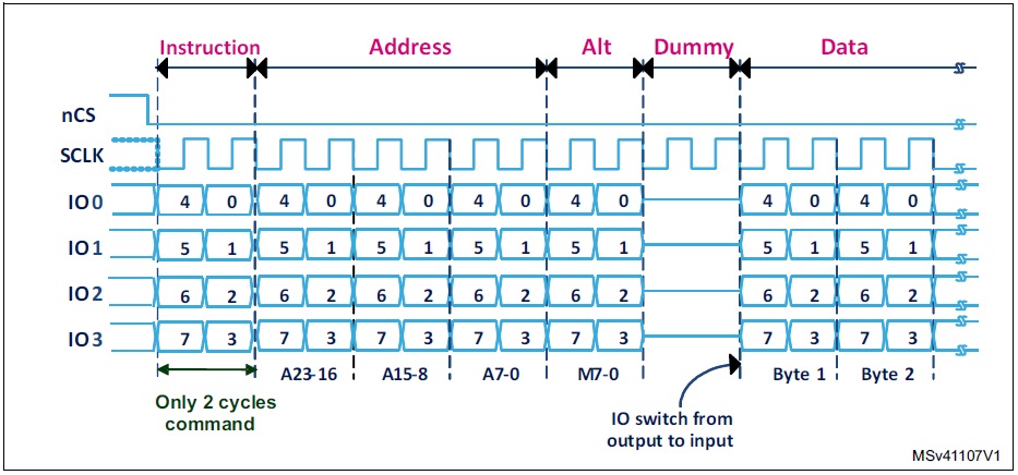
I didn't find all the information in the TRM (despite of the 8059 pages) needed to develop the QSPI drivers when the master is configured to receive data on the 4 lines.
The Master (AM572x) sends a command to the Slave (FPGA) to read a block of memory.
1. The line D0 need to switch from output to input after sending the command. What is the expected delay (1 clock period ?)
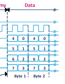
2. The memory shared into the FPGA is organized with 32-bits data words. Do you have any information regarding the Read sequence when the 4 lines are used. Is the sequence look like the following picture:
Regards,
Sylvain.