This thread has been locked.

If you have a related question, please click the "Ask a related question" button in the top right corner. The newly created question will be automatically linked to this question.

Sync EMIF turnaround time

According to EMIF user guide (chapter 6), the turnaround time for back to back sync read is 0, 0 for back to back sync write, and 1 for sync write followed by sync read.

Sync EMIF timing that I captured didn't follow the user guide. Any idea why?

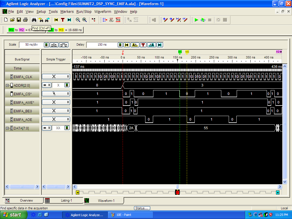
My CEnCFG setting is 0x8000020e (R_LTNCY = 3, W_LTNCY = 0, CS goes active until SOE goes inactive)

Attached is my captured sync EMIF signals. I did 3 back to back sync writes, followed by 3 back to back sync reads.

- There are 7 clock cycles in between back to back sync read.

- There is 0 clock cycle in between sync write and sync read

- There is 1 clock cycle in between back to back sync write


Thanks.

  • Most of what you see is probably coming from the DSP signal sequencing delays rather than the EMIF activity itself. Try the _amem8 intrinsic to read a 64-bit double-word and you will see true back-to-back reads for that access. Otherwise, the DSP starts the read request internally and waits until it gets the data back before continuing to the next read.

    The most efficient use of the EMIF is done by the EDMA since it can generate bursts of reads or writes, unlike the DSP code.

    Since there is a delay between when the DSP drives the bus for the last write and when the memory device drives the bus for the first read, AWE to AOE (SOE?), the required turnaround time is achieved.

    Regards,
    RandyP


    If this answers your question, please click the  Verify Answer  button below. If not, please reply back with more information.

  • Randy

    The code I am using to implement this functionality is as follows;
     

    unsigned char * restrict pEmifaDataTemp = (unsigned char *)emifaAddr; //intrinsic test pointer

    volatile long long tempData2 = 0;

    tempData2 = _amem8(pEmifaDataTemp);

    tempData2 = _amem8(pEmifaDataTemp);


    I have my EMIFA config set up for a read latency of 1, a bus size of 32-bits, and CE active when SOE is active.

    CE5CFG = 0x80000246;

    When I run the code, I only see one read access occur on my LA and while CE and SOE are asserted, I am seeing the address bus transition after the first cycle into the access.

    Is the above code snippet the correct way to implement the back-to-back read accesses you are refering to?

    Thanks


    Tom

  • Tom,

    For the prupose of closure, I'd like to wrap up this post. Since I worked with you directly on this issue, I'd like to summarize and then if you have anything to add please do so. This way if anybody else comes across this thread, is doens't end suddenly.

    The assembly output of the code you provided above does indeed show multiple instructions between the two intrinsics (LDDW instructions). This is one cause of delay between them. Even if the two LDDW instructions were back to back, you would still see some delay between them as Randy pointed out. To -really- burst to/from the EMIF, you need to use somethig like the EDMA. I'll go ahead and past in the C code to kick off a QDMA that I sent to you for others to reference.


    #include <stdio.h>

    #include <stdlib.h>

    #include <string.h>


    // shortcut macros for reading/writing to 32-bit memory mapped registers

    #define REG32(addr) *(volatile unsigned int *)(addr)


    unsigned char srcBuff[1024];

    unsigned char dstBuff[1024];


    void main() {


      unsigned int paramAddr;


      printf("QDMA Example %s %s\n",__DATE__,__TIME__);


      //------------------------------------------------------------

      // setup a simple QDMA channel to do a linear block copy

      //------------------------------------------------------------


      // we'll use PaRAM number 64 (this is an arbitrary number)

      paramAddr = 0x02A04000 + 64*32;


      // zero out the PaRAM entry

      memset((void*)paramAddr, 0x00, 32);


      // we'll use QDMA channel 0


      // map QDMA channel 0 to PaRAM 64 and set trigger word to 7

      REG32(0x02A00200 /*QCHMAP0*/) = (/*PAENTRY*/ 64 << 5) | (/*TRWORD*/  7 << 2);


      // enable the QDMA channel

      REG32(0x02A0108C /*QEESR*/) = 0x00000001;


      // program up the QDMA PaRAM values

      REG32(paramAddr+0  /*OPT             */) = 0x00000008;

      REG32(paramAddr+4  /*SRC             */) = (unsigned int)srcBuff;  // change this to something out in CE5

      REG32(paramAddr+8  /*BCNT_ACNT       */) = (/*BCNT*/ 1 << 16) | (/*ACNT*/ 64);

      REG32(paramAddr+12 /*DST             */) = (unsigned int)dstBuff;

      REG32(paramAddr+16 /*DSTBIDX_SRCBIDX */) = (/*DSTBIDX*/ 0 << 16) | (/*SRCBIDX*/ 0);

      REG32(paramAddr+20 /*BCNTRLD_LINK    */) = (/*BCNTRLD*/ 0 << 16) | (/*LINK*/ 0);

      REG32(paramAddr+24 /*DSTCIDX_SRCCIDX */) = (/*DSTCIDX*/ 0 << 16) | (/*SRCCIDX*/ 0);


      // writing to word 7 (numbered 0 through 7) is the trigger word and will kick off the transfer

      REG32(paramAddr+28 /*RSVD_CCNT       */) = (/*RSVD*/ 0 << 16) | (/*CCNT*/ 1);

    }