This thread has been locked.

If you have a related question, please click the "Ask a related question" button in the top right corner. The newly created question will be automatically linked to this question.

OMAP138/TMS320C6748 and 2G bit NAND flash

Other Parts Discussed in Thread: TMS320C6748

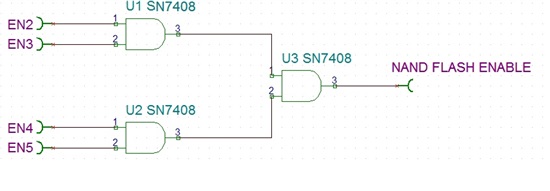
The NAND memory space could be accessed by CS3 of TMS320C6748 is only 32MB x 8 = 256Mbit wide.

I only want to use one single NAND with 2Gbit memory space.

How I can use other chip enable pins such as CS2, CS4 and CS5 to access the rest memory space of 2G bit NAND flash?

I want to use a CPLD to interface between TMS320C6748 and NAND, but I am afraid the timing will be bad.

Please help.

Thanks in advance.


  • If you have a CPLD in between the device and the NAND, then you should be able to create a solution that allows this. It would have have to look at which chip select is active and modify the data to form the correct address.

    As for the timings, as long as you can match the delays between all the input and output pins, the sustained throughput should be equivalent to a direct connect. The read latency will be affected by how much delay the CPLD adds though.

    Jeff

  • Thank you for your answer.

    I plan to use discrete AND gate chips to enable this single NAND FLASH.

    I have checked the asynchronous memory read timing and asynchronous memory write timing on page 119 of TMS320C6748 datasheet, looks like the propagation delay ( max 4 ns) generated by AND gate chips don't have too much bad effect on NAND Flash timing.

    How do you think this way?

    Thank you again.

    The attached image shows my NAND Flash chip enable plan:


  • Can you give more details on what you mean by this?

    Jeff