Hi,TI team
I am using SDK1.0 sample code to debug 8D8D8D mode of CYPRESS S28HS512T Flash chip, that is, OCTAL DDR mode:
When I set the value of an 8-bit flash register to 03, I went to read the value of this register. Since I did not get the correct value after reading 1 byte, I read back three bytes and the value is 00 03 03, and the correct value of my register is 03; when I set the register value to 08, the value read back is 000808; when I set the register value to C0, the value read back is 00C0C0;
When I read the flash ID, I have set a dummy cycle that matches the clock in advance. The correct value of the ID should be 34 5B 1A 0F 03, and the value I read back is 00 34 5B 1A 0F.
From the above phenomenon, every time I read the value, there is an additional clock edge which causes my data to be wrong.I have the following two questions:
1.In DDR mode, both rising and falling edges capture data. How can I configure it to
read odd-numbered data?
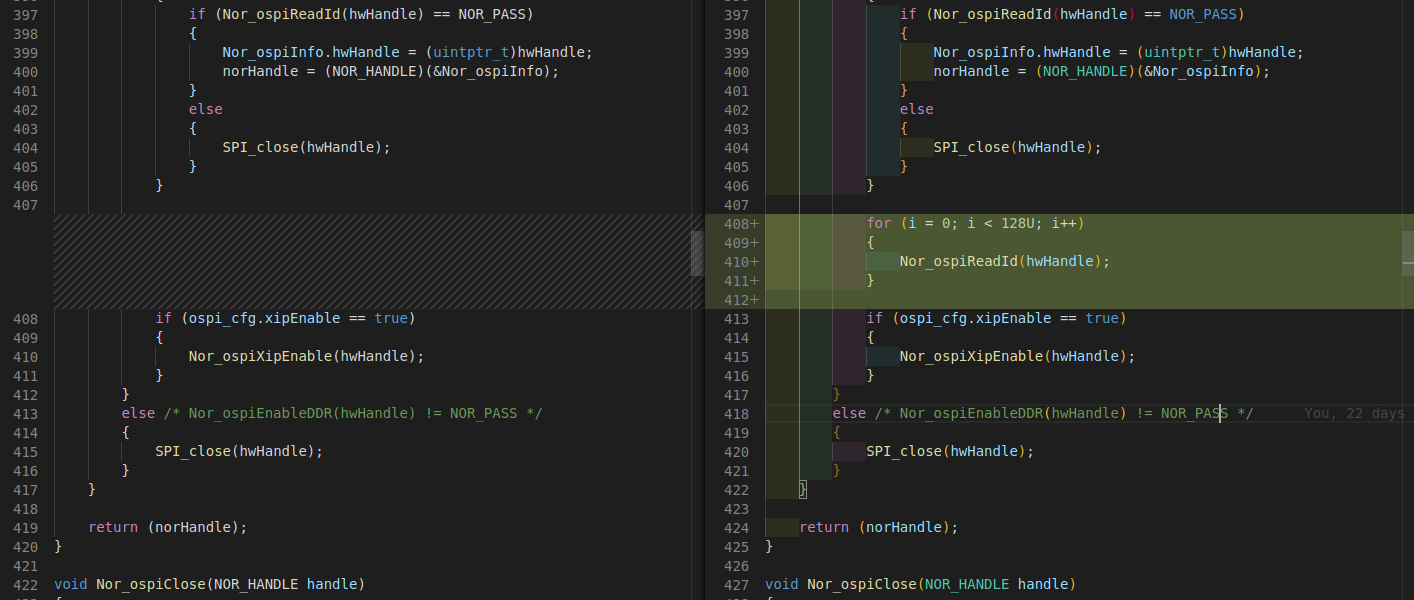
2.In addition, when the SDK package I am using to read the flash ID, no matter which mode is used, the number of bytes for reading the ID cannot be even. What is the reason?
Look forward to your reply.