Hi,
I have questions about DDR PHY controller for AM335x
Q1: WR_DQS_SLAVE_RATIO_CS0 seems to be the amount of shift of the DQS signal from the DQ signal output at write access.
Which signal does WR_DATA_SLAVE_RATIO_CS0 indicate the amount of shift?
Q2: What is the meaning of the DATA0/DATA1_REG_PHY_DQ_OFFSET_0 register setting value?
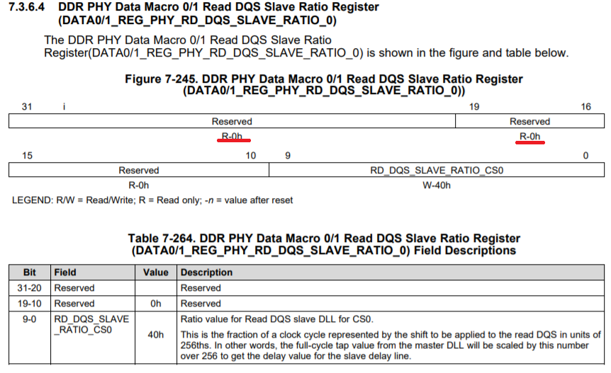
Q3:What is the meaning of the RD_DQS_SLAVE_RATIO_CS0 register setting value?
What is the relationship between the master DLL and the slave DLL as described in the description of this register?
Q4:The reset value of DATA0_REG_PHY_RD_DQS_SLAVE_RATIO _0 is listed in Table 7-260 as 0x04010040.
On the other hand, the reset value is different from the one shown in Figure 7-245; what is the difference?
Best Regards,
H.U


