This thread has been locked.

If you have a related question, please click the "Ask a related question" button in the top right corner. The newly created question will be automatically linked to this question.

OMAP1621 interface with Parallel NOR FLash

Hi

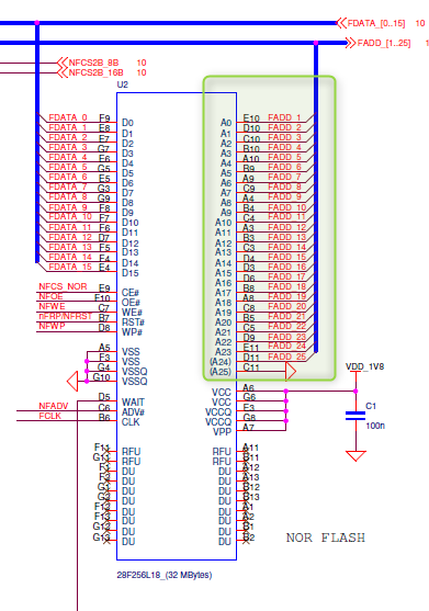
In one of design uses OMAP1621 with NOR FLASH Interface .

With CS3 as chip select ,we use 8M x 16bit   parallel flash 

The NOR FLash Addressing is FLASH.ADDRESS[25:1] .The interface used is 16 bit data .

Is l Flash Address A1 a least significant bit or shall have A0 assigned from OMAP processor .?

  • Hello,

    I've attached a fragment of a schematic for an OMAP16xx to a parallel NOR for a board I know to work.  The SOC A1 goes to the flash A0.

  • Hi ,

    I have added test-point for A0 and A1 of memory .

    When read address location ,Ao and A1 is read as below : 

    ReadAddress  CS3 

    Flash Address (FADD) 

    MemAddrA1 

    (FADD2) 

    Mem  Addr A0 (FADD1)
    0x0C000001 0 0
    0x0C000002 0 1
    0x0C000003 0 1
    0x0C000004 1 0
    0x0C000005 1 0
    0x0C000006 1 1
    0x0C000007 1 1
    0x0C000008 0 0

    From Above table the It is understood that FADD is shift Right by 1 .Which means FADD can not have A0  means A1 is LSbit and means can read as 1x 16 only .Unlike in the block diagram shared by you ,Does it mean that FADD1 shall be connected A1 of  memory and odd location can not be refernced directly

    byte reading not possible  for example 5th location 101 binary will be sent as 010 binary so location may be 4 where MSB of data is 5th location byte.

    Since my board is based on the block diagram whenever I access the memory I need to shift left to compensate the shift right in omap as is 1 x16.

    Please advice. 

  • Your table looks correct to me since the Flash has a 16-bit data bus, and the OMAP161x supports byte addressing internally. The odd addresses correspond to the upper byte D[15 - 8], but the interface does not support byte addressing. For example address 0xC000000 and 0xC000001 both access the same 16-bit word which contains the odd and even byte.

    In s/w your accesses to the Flash must always be even-byte aligned since the interface is reading two bytes at a time. To isolate the upper byte, S/W must manipulate the 16-bit data by performing shift or logic operations, etc. 

  • Hi Richard ,

    Thanks for the input .In TRM I could see as below :

    image.png