


Other Parts Discussed in Thread: CDCM6208
I am experimenting with the EVMK2EX board to create a PCIe Root Complex using PCIe-0 through the AMC. We confirmed that Pin 80 and pin 81 (FCLKA-/A+) are receiving 10 ns clock from an RDK switch, using a x1 lane SMA connection. The clock signals from SMA's pin 13/14 are connected to AMC's FCLKA+/FCLKA-.
My VxWorks driver is failing to establish PCIe link. There may be several reasons for the failure, so I wanted to first confirm the Clock signal propagation from the SoC to AMC.
Kindly let me know how the correct clock signal can be configured. The TRM and Schematics refer to BMC (TI LMS2D93), but other than TRM's Section 2.7 sentence that the LMS2D93 registers are accessible through SPI interface, I haven't found a reference to how the MUX can select AMC's FCLKA+/A-. Please point me to appropriate references.
Following diagrams are from the "EVMK2E Technical Reference Manual" spruin5.pdf
Figure 2.4 EVMK2E Clock Domains shows a Mux that controls which clock signal (from AMC / from CDCM6208) reaches SoC's PCIe-0_CLKP/N pair.
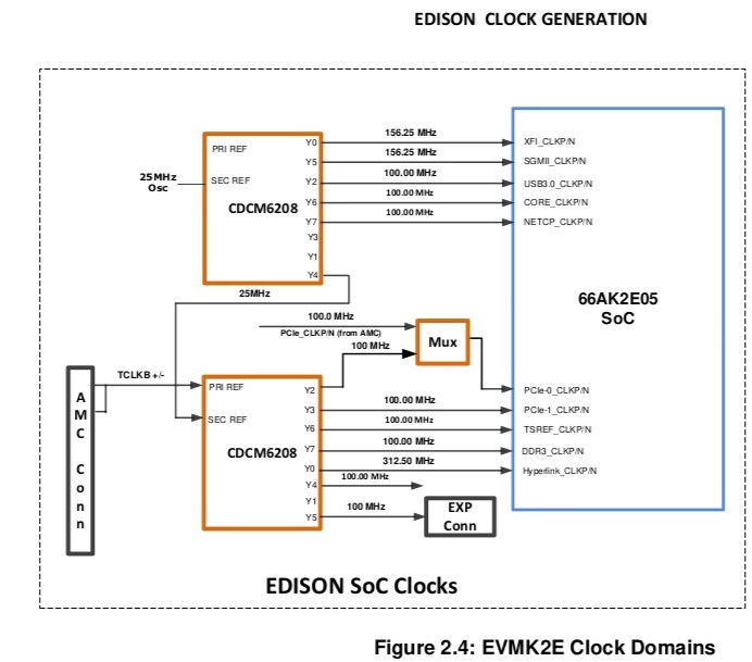
Based on eInfoChip's K2E_EVM_SCH_16_00175_03.pdf page 19, the IDT5V41068 PCI Clock Mux selects source of PCIE0CLKP_M/N_M pair.

Thanks,
Subodh
