This thread has been locked.

If you have a related question, please click the "Ask a related question" button in the top right corner. The newly created question will be automatically linked to this question.

Why there is so much polygon area on EVM6437 layout?

Anonymous
Anonymous


Hi All,


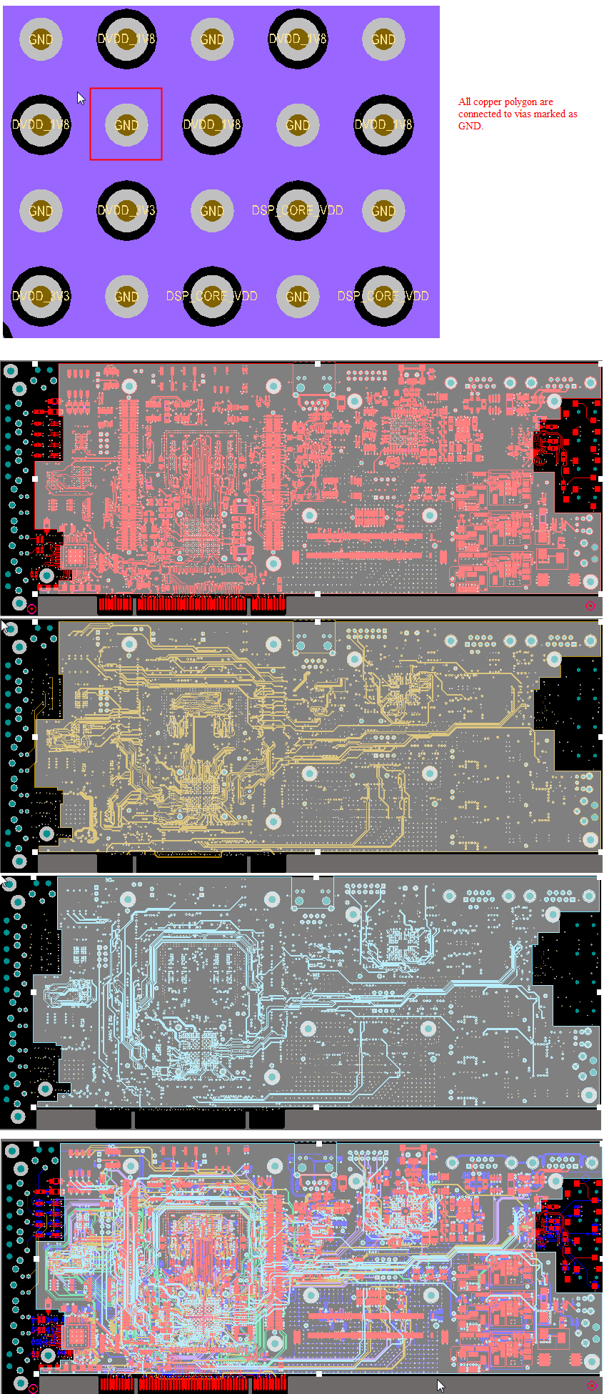
I have found that with the EVM6437 board which I am studying, in all layers there are large area of polygons which has areas dozens of times to that of tracks.


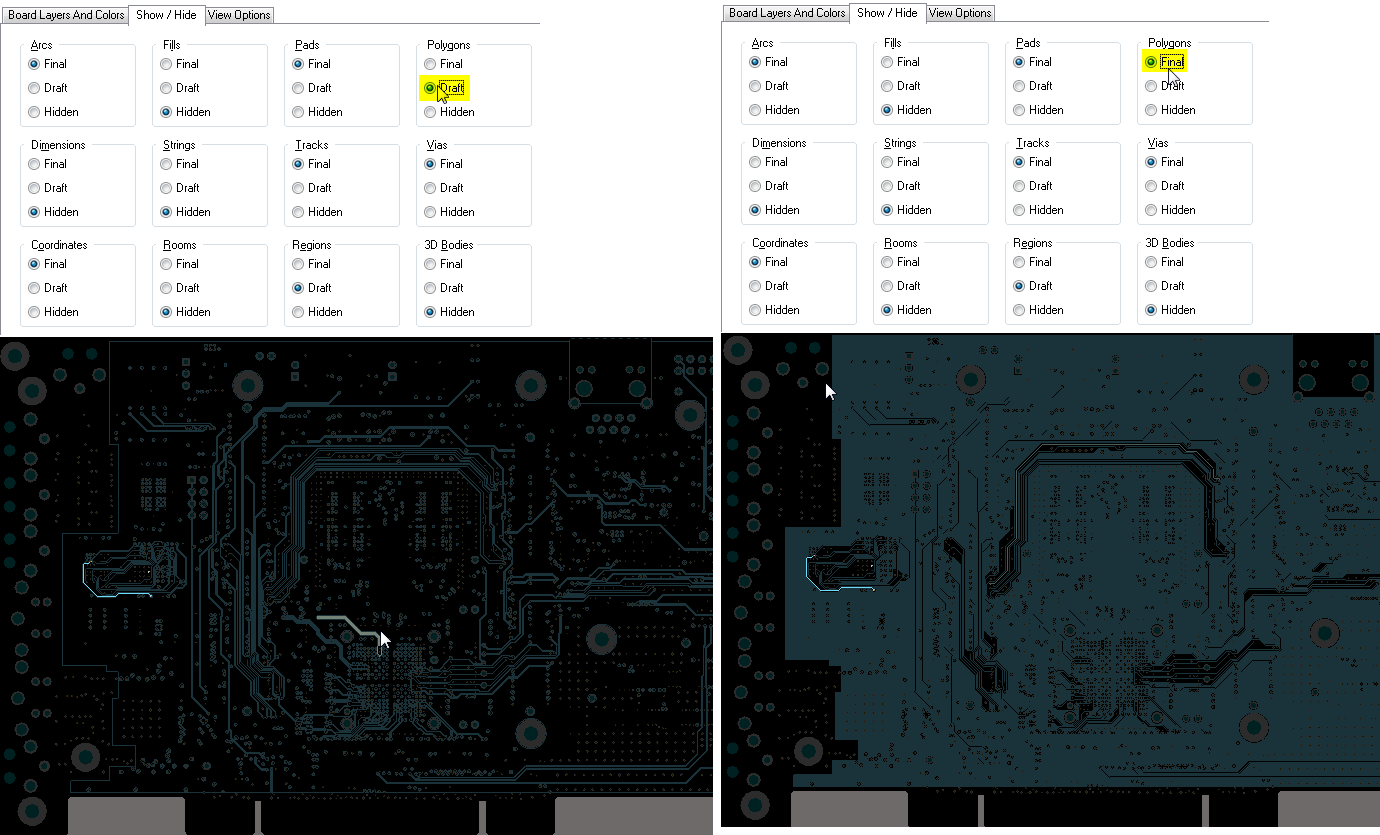
The attached picture show a comparison on Mid-layer 2 when Polygon display is switched between "draft" and "final", and the difference is clear.


I searched and read some articles on the Internet about polygon areas in PCB, but still haven't understood it well.


Isn't that tracks themselves alone are sufficient for carrying signals? Some large areas of copper might be useful on power or ground planes, as well as for EM shielding. However, why on all SIGNAL layers do there exist such large areas of polygon (copper?), which gives the impression that they are primary and the tracks are secondary?


My view is that if tracks are needed, some small portion would be enough, and they ought to be mostly on power/ground planes. But why there are so much of them, to the extent that they are the predominant, on all signal layers of the board?


Hope someone could help with this.


Zheng


  •  

    Adding to the previous question:

    This first newly attached picture shows the polygon on several layers. The top sub-picture is the zoom-in view of an area on mid layer 2, and in this view it can be seen that the all GND vias are connected to the copper polygon fill.


    The following figures shows the transparent polygon overlaid on


    as well as all six signals (adding Mid-layer 4 & Bottom layer) shown together.


    And the second newly attached figure shows the board's three internal layers.


    My question is still on the purpose of polygon layer.


    In the first sub-figure of the newly attached figure 1, and in fact in all signal layers, large areas of polygon fill are solely connected to GND vias. But why no polygon fill with VCC vias?


    Shouldn't they be symmetric? What is the purpose of polygon layers?


    I.

    By the simple formula for resistance calculation, R= ρl/A, in which

    ρ: resistivity

    l:  length

    A: area


    For large area of copper polygon, we can generally regard its effect as increasing A, and hence reducing the resistance. At the mean time, since by Joule's law:

    P=I2R

    Since I is usually fixed, so P R P 1/A


    And when P is generated over the whole sectional area A, then for each unit area, its heat power density 1/A2.  Therefore, it is clear that the larger A is, the less temperature rise there will be and circuit hence would be more reliable.


    Since all components in the board needs to be connected to the ground, there will be much current flowing to the ground, and it might be necessary to minimize heat by increasing the sectional area A, as just reasoned.


    What I could not understand was why there is no corresponding polygon fill for Vcc vias? In an argument almost the same as for GND, there will also be much current through power source’s high voltage. Why there is no heat concern, and hence the polygon fill?


    II.

    Another perspective is from voltage. As mentioned before, R 1/A, and V = IR. The smaller R is, the closer V is to zero. So if there is requirement that a component (or it is a general rule for most or all components) that the Vss pin should be connected to zero voltage, then it is necessary to make the R between Vss pin and GND as small as possible. To achieve this, one way is to increase R’s sectional area A, and the polygon copper fill is an implementation.


    Which one is the real reason for polygon fill? If none is correct, what is the reason then?


    Could anyone help with this?


    Thanks,

    Zheng


  • Anonymous
    0 Anonymous in reply to Anonymous

    Hi,

    I read some material and tend to believe that the purpose of these large area of polygon is to prevent "ground bounce".

    http://en.wikipedia.org/wiki/Ground_bounce said:

    Ground bounce is usually seen on high density VLSI where insufficient precautions have been taken to supply a logic gate with a sufficiently low resistance connection (or sufficiently high capacitance) to ground. In this phenomenon, when the gate is turned on, enough current flows through the emitter-collector circuit that the silicon in the immediate vicinity of the emitter is pulled high, sometimes by several volts, thus raising the local ground, as perceived by the transistor, to a value significantly above true ground. Relative to this local ground, the BASE voltage can go negative, thus shutting off the transistor. As the excess local charge dissipates, the transistor turns back on, possibly causing a repeat of the phenomenon, sometimes up to a half-dozen bounces.


    Could anyone confirm this?


    Thanks,

    Zheng