This thread has been locked.

If you have a related question, please click the "Ask a related question" button in the top right corner. The newly created question will be automatically linked to this question.

AM3358: Touch screen Pen touch detect resistance requirement

Part Number: AM3358

Hi, Expert,

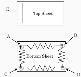
In the AM3358 datasheet, table Table 5-16. TSC_ADC Electrical Parameters, there is maximum pen touch detection resistance specification which is 2K Ohm. What is the definition of this resistance? is it the resistance measured from the TSC_SENSE to any of the other 4 pins  for 5-wire touch screen?

If one touch screen have resistance larger than 2K ohm measured from TSC_SENSE to any of the other 4 pins, say 3K Ohm, what is the consequence of this? will pen-touch event be missed ? or ADC measurement result will be affected? if pen-touch event detection is not affected, can we elongate the open-delay to get an accurate ADC reading?

Thanks,

Peng.

  • Hi Peng,

    Yes, the 5th Wire resistance measurement would be at the point of Point "E". If you're scanning the X axis, AC would be HIGH potential while BD would be GND, AB & CD respectively would be that for Y axis scanning. 


    If the value exceeds the datasheet Max value of 2K then it is an unsupported use case, most likely you will have a missed touch event. 

    Please let me know if this helps answer your question. 

    Regards,

    Andrei

  • The AM335x touch screen controller has an internal pull-up that gets pulled low when there is a pen down event. If the combined resistance of the panel and any connectivity to AM335x is too high, the internal pull-up would not be pulled low enough to trigger the interrupt. The 2k limit is from the AM335x ADC input pin to VSS.

    Regards,
    Paul

  • I just realized my comment about the 2k limit to VSS may be confusing. The path from the interrupt input to VSS is from TSC_SENSE though the panel back to VSS via one or more of the other ADC pins which are configured to be connected to VSS.

    Regards,
    Paul

  • Thanks Andrei and Paul,

    I did some experiment and observed that the pen-down interrupt is not missed when the pen touch detect resistance is about 2.4 KOhm. 

    But the readout value has big deviation with Open-delay value of  456 which means the delay is about 1.82us before the ADC sampling. On the circuit board, I have only 200pF filtering capacitance, i.e. RC time constant is about 2.4KX200p=0.5us.  So I think 1.8us Open-delay should be enough.

    We also increased Open-delay to far larger value than 456, then it seems the readout value deviation is becoming smaller.

    So does this mean there is another big capacitance in the touch panel or AM3358 TSC ADC I don't consider?

    What is the monitored pen-down event voltage threshold value? we can change this threshold by SW?

    And although pen touch detection resistance is bigger than 2KOhm, if the pen touch event is not missed, it is still OK to use those touch panels with bigger touch detect resistance?

    Peng

  • What frequency is your ADC clock?  The ADC clock needs to be greater than 1MHz to ensure the conversion period is short enough that the voltage applied the sampling capacitor doesn't bleed-off due to internal leakage paths before the conversion is complete. I have seen the ADC give erratic values when the ADC clock is too slow.

    I assume you are performing single-ended measurements. If so, have you configured SEL_INM_SWC to a value of 0x8h so the ADC negative input is referenced to VREFN while connecting the ADC positive input to the appropriate input with SEL_INP_SWC?

    The ADC input only has about 10.5 pF of capacitance. The panel may have capacitance, but you would need to ask the manufacture for a value.

    I have not seen the pen-down interrupt threshold discussed in any internal documents. We define minimum resistance as the control point for proper operation of the interrupt. So the interrupt threshold is not typically needed when the system designer has selected a panel that is compliant to the minimum resistance requirement. The interrupt threshold is a fixed value that has not been characterized and I'm fairly sure the minimum resistance value is based on simulations using worst case conditions.

    I do not have any sense for how much margin was designed into everything that can affect touch screen operation. Therefore, I can only recommend you to use a panel that is compliant to the requirement.

    Regards,
    Paul

  • Hi, Paul,

    Thanks for you detail reply.

    I checked with our SW engineer. The ADC clock is 3MHz. The measurement is single-ended with ADC negative input connected to VREFN.

    Since the touch panel datasheet says its biggest pen touch detect resistance is 3K Ohm, I did experiment to insert series resistor in the pen touch detect signal network to make the resistance more than 4K Ohm, the TSC works fine and can detect each press event.

    For the the panel parasitic capacitance, I asked our touch panel vendor, but the hasn't received feedback. For AM3358, if the pen touch detect resistance is kept within 2KOhm, what is the maximum parasitic capacitance it can support? and how to calculate the open-delay based on the pen touch detect resistance and the parasitic capacitance?

    Regards,

    Peng

  • TI cannot answer this question since your software will need to be customized to find middle ground between what works reliably with the touch panel you selected while providing expected user experience. The response time of your software may not create a good user experience if the touch panel resistance is too high and you slow the signals even further with external filters. It is up to the system designer to customize software delays to achieve reliable performance for your specific hardware configuration while providing expected user experience.

    I want to remind you the open-delay only inserts a delay before the acquisition begins.

    The sample-delay is what controls how long the sample capacitor is connected to the source during acquisition. The sample capacitor will be connected to the source for a minimum of two clock periods which is about 667 ns when using a 3 MHz ADC clock.

    As I mentioned before, the ADC only has about 10.5 pF of input capacitance which should not be a limiting factor even for a 4k resistive panel. The RC time constant of a 4k resistive panel changing a 10.5 pF capacitor is about 42 ns. So the sampling capacitor will be very close to fully changed since there is over 15 RC time constants in two ADC clock cycles.

    Regards,
    Paul

  • Hi, Paul,

    We did some adjustment on sample-delay, and found that increasing this Sample-Delay can provide better TSC ADC response.

    The default value of SampleDelayis 0 in STEPDELAYx Register which means 1 ADC CLOCK sample-delay. So does your comment "The sample capacitor will be connected to the source for a minimum of two clock periods which is about 667 ns when using a 3 MHz ADC clock." mean that the SampleDelay should be set at least 1 in the STEPDELAYx Register to provide at least 2 ADC clocks sample-delay? I didn't find any hint in the AM335X Technical Reference Manual that this Sample-Delay be at least 2 ADC clocks.

    Thanks,

    Peng

  • This information is defined in the TSC_ADC Electrical Parameters table provided in the AM335x datasheet. The parameter name is "Acquisition Time" and the min value represents the default value of sample-delay.

    Regards,
    Paul

  • Hi, Paul,

    The TSC_ADC Electrical Parameters table in the datasheet  shows the Acquisition Time is 2 ADC clock cycles min, and 257 ADC clock cycles max.

    However per AM335X Technical Reference Manual, SampleDelay is 8-bit.  So according to its description in STEPDELAYx register ---- "This register will control the number of ADC clock cycles to sample (hold SOC high). Any value programmed here will be added to the minimum requirement of 1 clock cycle." the maximum ADC clock cycles is 256, not 257. Seems there is a gap here?

    Regards,

    Peng

  • The description provided in the TRM was written by the digital state-machine designer and describes how his circuit works. I suspect he did not know the ADC connects the sampling capacitor to the input for one additional ADC clock cycle.  So acquisition time is (SampleDelay + 2) ADC clocks.

    Regards,
    Paul

  • Hi, Paul,

    So even I set SampleDelay as 0 in the STEPDELAYx register, the actual sample time is 0+2=2 ADC clocks, right?

    In what situation, should I increase the value of SampleDelay? it seems that bigger SampleDelay value can deliver more stable ADC readout.

    Thanks,

    Peng,

  • It is important for you to understand the output impedance of the source connected to the ADC analog input. The voltage captured on the sampling capacitor is a function of the output impedance of the source, input capacitance of the ADC, and acquisition period. The sampling capacitor will begin to charge or discharge to the applied voltage at the beginning of the acquisition period. If your acquisition period is too short, the capacitor may not have enough time to reach the desired voltage before the acquisition period ends and the conversion begins. Therefore, you should calculate the time required for the input capacitance to charge to desired accuracy based on the source impedance. There is no benefit in configuring the acquisition period much longer than necessary to fully change the input capacitance.

    Note: There is two components to the ADC input capacitance. The actual sampling capacitor is about 5.5pF, but there is another 5pF of parasitic capacitance that gets applied when the analog multiplexer selects one of the 8 inputs. If OpenDelay is zero, the analog multiplexer selects the appropriate input at the same time acquisition begins. The total input capacitance applied to the source at the beginning of the acquisition period in this case would be 10.5pF, so you should use 10.5pF in your calculation to insure the sampling capacitor is fully charged.

    Regards,
    Paul