This thread has been locked.

If you have a related question, please click the "Ask a related question" button in the top right corner. The newly created question will be automatically linked to this question.

Compiler/AM6548: TMDX654IDKEVM

Part Number: AM6548
Other Parts Discussed in Thread: SYSBIOS

Tool/software: TI C/C++ Compiler

Hello Experts,

If I could be pointed in the correct direction, please.

The below image is a screenshot of CCS. The top right red oval indicates a drop-down menu.
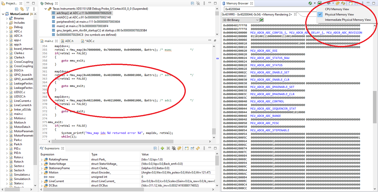
Question:

What is this?. What memory is this being associated with?

I have also indicated another oval to the bottom left, this is the RTOS "mapping".

At the risk of sounding completely daft, I'm assuming these drop-downs are related to virtual memory.

Question: If this is the case? Then where is the intermediate memory viewed from? What is this drop-down menu indicating/doing?.

Is this implying that the interconnect communication is implicitly happening by virtue that I have set up the RTOS function "Mmu_map" or do I need to set this up?

I am "writing" values to the ADC registers, but I am not completely convinced that I am. Sometimes I see it in CPU memory other times in physical memory, especially when single-stepping the software.

Thanks

Carl

  • Carl,

    You are correct that these memory view selections deal with virtual memory. The CPU memory view is the address seen by the CPU before translation and the physical memory view is at the memory (untranslated). Intermediate memory view shows the intermediate translation. The Arm MMU is a 2-stage lookup with stage 1 converting from CPU to intermediate and stage 2 converting from intermediate to physical. This allows for multiple OSs and hypervisor to run on the architecture, with the hypervisor controlling the second stage translation.

    Are you using the mmu_map to translate the address or only to set attributes?

    The MMU doesn't store the data, so your writes should propagate through unless they are landing directly in cache (if set as a cacheable region), in which case they may not be reflected at the physical memory.

    Best regards,

    Dave

  • Hello Dave,
    Thanks for the information.
    If my understanding is correct, the mmu function has four parameters I have set the "mapping" one to one with a size of 1000h.
    If I have digested your information correctly then the first parameter is most likely the CPU memory and the second parameter would be the device memory that sits wherever, yes?
    The mechanism that I have used is like below. So I'm thinking that I have used it to translate the address( 1: 1 )
    ////////////////////////////////////////////////////////////////////////////////////////////////////////////////////
    ////////////////////////////////////////////////////////////////////////////////////////////////////////////////////
    typedef struct
    {
    union
    {
    uint32_t REG;
    struct
    {
    uint32_t step_idle : 5; // 10h = Idle 0h - Fh = Corresponds to Step 1 - Step 16
    uint32_t fsm_busy : 1; // ADC_STATUS of FSM. 0h = Idle 1h = Conversion in progress
    uint32_t mem_init_done : 1; // ADC_STATUS of RAM initialization for ECC. 1h = RAM initialization to 0 after reset is done.
    uint32_t reserved : 25;
    }FIELD;
    }DATA;
    }ADC_SEQUENCER_STAT;
    #define ADC0_SEQUENCER_STAT ( *( (volatile ADC_SEQUENCER_STAT* )0x40200044) )
    #define ADC1_SEQUENCER_STAT ( *( (volatile ADC_SEQUENCER_STAT* )0x40210044) )

    So essentially if I see the data being, reflected in the physical memory display area then this means that it is physically there at the hardware end, which in this case is the ADC.
    As for the attribute, maybe I have missed a trick here. I have just used the attributes that sat in the Void InitMmu() function..part of the template RTOS AM65xx. I have not found information on the mmu function.
    But think have answered the question ...
    Thanks
    Carl

  • Can you show us the line from InitMmu where you map the ADC?

  • Carl,

    Please do confirm. If you're setting an MMU section for control registers you'll want to be sure they're not cacheable. Address translation is likewise not required, and for basic applications your vaddress and paddress can be the same.

    e.g. below for config MMR entry and MSMC SRAM entry

    void InitMmu(void)
    {
    bool retVal;
    uint32_t mapIdx = 0;
    Mmu_MapAttrs attrs;

    Mmu_initMapAttrs(&attrs);

    attrs.attrIndx = 0; //non-gathering, non-reordering and no early write acknowledegement

    retVal = Mmu_map(0x00100000, 0x00100000, 0x00900000, &attrs); /* Main MMR0 cfg */
    if(retVal == FALSE)
    {
    goto mmu_exit;
    }

    ...

    attrs.attrIndx = 7; // normal outer and inner write-back cacheable non-transient memory
    mapIdx++;
    retVal = Mmu_map(0x70000000, 0x70000000, 0x04000000, &attrs); /* msmc */
    if (retVal == FALSE)
    {
    goto mmu_exit;
    }

    ...

    Best regards,

    Dave

  • Hello Dave and Dominic

    Thanks for that...

    I can confirm that I have been setting the "attrs.attrIndx = 7"

    The domain is MCU  so I will change it to 0.

    Where can I glean this information from with regards to how the processor deals with the attribute features do you guys have this or do I get it from Arm.

    Kind Regards

    Carl

  • Hello Carl,

    Carl Rainbird said:
    The domain is MCU  so I will change it to 0.

    Setting the memory attribute index to 0 would be the right thing to do, but this has nothing to do with your target peripheral being in the MCU domain (as opposed to MAIN domain, if that's what you're thinking of).

    The important information is in the comments from Dave's code snippets:

    attrs.attrIndx = 0; //non-gathering, non-reordering and no early write acknowledegement

    attrs.attrIndx = 7; // normal outer and inner write-back cacheable non-transient memory

    TI-RTOS / SYS-BIOS configures the A53 in a way so that memory attribute index (MAI) 0 has non-gathering, non-reordering, no early-write-acknowledge (nGnRnE) behaviour. On previous ARM architectures this used to be called "strongly ordered". The memory system ensures that every access performed by the CPU appears in exactly the same order and width on the bus, and it waits even for a write to complete (writing could also be "fire and forget").

    MAI 7 on the other hand is configured as "normal" memory, that is GRE: gathering, reordering, early-write-ack, and in addition the memory is marked as outer and inner write-back cacheable. The memory system is basically allowed to use all available optimizations to improve throughput.

    For peripheral registers, no matter which AM6x device domain they live in, you need to know that the access happen in the exact order etc., so you'd use MAI 0.

    The available MAI indices are defined by the operating system (TI-RTOS) in your case. You can find this in the installed SDK at .../ti/bios_6_82_01_19/docs/cdoc/ti/sysbios/family/arm/v8a/Mmu.html#.M.A.I.R0

    In order to understand the meaning you should look into the ARM v8A architecture reference manual.

    Regards,

    Dominic

  • Hello Dominic

    Thanks for that additional information, I appreciate it.

    Hopefully, the links will shed some better understanding on my part..so many pot-holes that need filling in on my part.


    Kind Regards

    Carl