


Hi:
We have a custom board running on linux which has a FPGA connnected to the GPMC in address and data multiplexed mode.It seems we can write FPGA successfully, however only 0x0 can be read from it.
Here is our dts file:
    sram_x16_default: sram_x16_default {
		pinctrl-single,pins = <
			AM33XX_IOPAD(0x800, (PIN_INPUT_PULLUP | MUX_MODE0))  /* gpmc_ad0.gpmc_ad0*/
			AM33XX_IOPAD(0x804, (PIN_INPUT_PULLUP | MUX_MODE0))  /* gpmc_ad1.gpmc_ad1*/
			AM33XX_IOPAD(0x808, (PIN_INPUT_PULLUP | MUX_MODE0))  /* gpmc_ad2.gpmc_ad2*/
			AM33XX_IOPAD(0x80c, (PIN_INPUT_PULLUP | MUX_MODE0))  /* gpmc_ad3.gpmc_ad3*/
			AM33XX_IOPAD(0x810, (PIN_INPUT_PULLUP | MUX_MODE0))  /* gpmc_ad4.gpmc_ad4*/
			AM33XX_IOPAD(0x814, (PIN_INPUT_PULLUP | MUX_MODE0))  /* gpmc_ad5.gpmc_ad5*/
			AM33XX_IOPAD(0x818, (PIN_INPUT_PULLUP | MUX_MODE0))  /* gpmc_ad6.gpmc_ad6*/
			AM33XX_IOPAD(0x81c, (PIN_INPUT_PULLUP | MUX_MODE0))  /* gpmc_ad7.gpmc_ad7*/
			AM33XX_IOPAD(0x820, (PIN_INPUT_PULLUP | MUX_MODE0))  /* gpmc_ad8.gpmc_ad8*/
			AM33XX_IOPAD(0x824, (PIN_INPUT_PULLUP | MUX_MODE0))  /* gpmc_ad9.gpmc_ad9*/
			AM33XX_IOPAD(0x828, (PIN_INPUT_PULLUP | MUX_MODE0))  /* gpmc_ad10.gpmc_ad10*/
			AM33XX_IOPAD(0x82c, (PIN_INPUT_PULLUP | MUX_MODE0))  /* gpmc_ad11.gpmc_ad11*/
			AM33XX_IOPAD(0x830, (PIN_INPUT_PULLUP | MUX_MODE0))  /* gpmc_ad12.gpmc_ad12*/
			AM33XX_IOPAD(0x834, (PIN_INPUT_PULLUP | MUX_MODE0))  /* gpmc_ad13.gpmc_ad13*/
			AM33XX_IOPAD(0x838, (PIN_INPUT_PULLUP | MUX_MODE0))  /* gpmc_ad14.gpmc_ad14*/
			AM33XX_IOPAD(0x83c, (PIN_INPUT_PULLUP | MUX_MODE0))  /* gpmc_ad15.gpmc_ad15*/

			AM33XX_IOPAD(0x870, (PIN_INPUT_PULLUP | MUX_MODE0))  /* gpmc_wait0.gpmc_wait0*/
 			AM33XX_IOPAD(0x874, (PIN_OUTPUT | MUX_MODE0))        /* gpmc_wpn */
 			AM33XX_IOPAD(0x87c, (PIN_OUTPUT | MUX_MODE0))       /* gpmc_csn0.gpmc_csn0 */
 			AM33XX_IOPAD(0x884, (PIN_OUTPUT | MUX_MODE0))       /* gpmc_csn2.gpmc_csn2 */
			AM33XX_IOPAD(0x88c, (PIN_OUTPUT | MUX_MODE0))       /* gpmc_clk */

			AM33XX_IOPAD(0x890, (PIN_OUTPUT | MUX_MODE0)) /* gpmc_advn_ale.gpmc_advn_ale */
			AM33XX_IOPAD(0x894, (PIN_OUTPUT | MUX_MODE0)) /* gpmc_oen_ren.gpmc_oen_ren */
			AM33XX_IOPAD(0x898, (PIN_OUTPUT | MUX_MODE0)) /* gpmc_wen.gpmc_wen */
			AM33XX_IOPAD(0x89c, (PIN_OUTPUT | MUX_MODE0)) /* gpmc_be0n_cle.gpmc_be0n_cle */
			>;
	};
&gpmc {
	status = "okay";
	pinctrl-names = "default";
	pinctrl-0 = <&sram_x16_default>;
        ranges = <0 0 0x08000000 0x01000000>;
        fpga@0,0 {
	        compatible = "mtd-ram";
		reg = <0 0 0x1000000>; // CS0, base_address, size of nor

		bank-width = <2>; // 16 bit
		gpmc,device-width = <2>; // 16 bit
		gpmc,mux-add-data = <2>; // address-data multiplexing

		// CS signals timings (num of GPMC_FCLK) corresponding to GPMC_CONFIG2
		gpmc,cs-on-ns = <0>; // Assertion time from start cycle time
		gpmc,cs-rd-off-ns = <186>; // De-assertion time from start cycle time for read accesses
		gpmc,cs-wr-off-ns = <186>; // De-assertion time from start cycle time for write accesses

		// ADV signal timings (num of GPMC_FCLK) corresponding to GPMC_CONFIG3
		gpmc,adv-on-ns = <12>;  // Assertion time from start cycle time
		gpmc,adv-rd-off-ns = <48>; // De-assertion time from start cycle time for read accesses
		gpmc,adv-wr-off-ns = <48>; // De-assertion time from start cycle time for write accesses

		// OE signals timings (num of GPMC_FCLK) corresponding to GPMC_CONFIG4
		gpmc,oe-on-ns = <54>; // Assertion time from start cycle time
		gpmc,oe-off-ns = <168>; // De-assertion time from start cycle time

		// WE signals timings (num of GPMC_FCLK) corresponding to GPMC_CONFIG4
		gpmc,we-on-ns = <54>; // Assertion time from start cycle time
		gpmc,we-off-ns = <168>; // De-assertion time from start cycle time

		// Access time and cycle time timings (num of GPMC_FCLK) corresponding to GPMC_CONFIG5
		gpmc,rd-cycle-ns = <186>; // Delay between start cycle time and first data valid
		gpmc,wr-cycle-ns = <186>; // Total write cycle time
		gpmc,access-ns = <114>;
		gpmc,page-burst-access-ns = <6>; // Delay between successive words in a multiple access

		// Access time and cycle time timings (num of GPMC_FCLK) corresponding to GPMC_CONFIG6
		gpmc,bus-turnaround-ns = <12>;  // Bus turn around latency between two successive accesses
										// to the same chip-select (read to write) or to a different
										// chip-select (read to read and read to write)

		gpmc,cycle2cycle-delay-ns = <18>; // Chip select high pulse delay between two successive accesses
		gpmc,wr-data-mux-bus-ns = <90>; // Specifies on which GPMC.FCLK rising edge the first data of the
										// synchronous burst write is driven in the add/data multiplexed bus.
		gpmc,wr-access-ns = <186>;  // Delay from StartAccessTime to the GPMC.FCLK rising edge corresponding
									// the the GPMC.CLK rising edge used by the attached memory for the first data capture.
		gpmc,cycle2cycle-samecsen;  // Add Cycle2CycleDelay between two successive accesses to the same chip-select (any access type)
		gpmc,cycle2cycle-diffcsen;  // Add Cycle2CycleDelay between two successive accesses to a different chip-select (any access type)

                gpmc,wait-on-read = "false";
                gpmc,wait-on-write = "false";
                gpmc,sync-read = "true";
                gpmc,sync-write = "true";

	        #address-cells = <1>;
	        #size-cells = <1>;
	};
};
And GPMC_CONFIG1~GPMC_CONFIG7 regs value are:
WRAPBURST: 0
READMULTIPLE: 0
READTYPE: 1
WRITEMULTIPLE: 0
WRITETYPE: 1
CLKACTIVATIONTIME: 00
ATTACHEDDEVICEPAGELENGTH: 00
WAITREADMONITORING: 0
WAITWRITEMONITORING: 0
WAITMONITORINGTIME: 00
WAITPINSELECT: 00
DEVICESIZE: 01
DEVICETYPE: 00
MUXADDDATA: 10
TIMEPARAGRANULARITY: 0
GPMCFCLKDIVIDER: 00
CSWROFFTIME: 10011
CSRDOFFTIME: 10011
CSEXTRADELAY: 0
CSONTIME: 0000
ADVAADMUXWROFFTIME: 000
ADVAADMUXRDOFFTIME: 000
ADVWROFFTIME: 00101
ADVRDOFFTIME: 00101
ADVEXTRADELAY: 0
ADVAADMUXONTIME: 000
ADVONTIME: 0010
WEOFFTIME: 10001
WEEXTRADELAY: 0
WEONTIME: 0110
OEAADMUXOFFTIME: 000
OEOFFTIME: 10001
OEEXTRADELAY: 0
OEAADMUXONTIME: 000
OEONTIME: 0110
PAGEBURSTACCESSTIME: 0001
RDACCESSTIME: 01100
WRCYCLETIME: 10011
RDCYCLETIME: 10011
WRACCESSTIME: 10011
WRDATAONADMUXBUS: 1001
CYCLE2CYCLEDELAY: 0010
CYCLE2CYCLESAMECSEN: 1
CYCLE2CYCLEDIFFCSEN: 1
BUSTURNAROUND: 0010
MASKADDRESS: 1111
CSVALID: 1
BASEADDRESS: 001000
Write 0x1234abcd to 0x8009600:
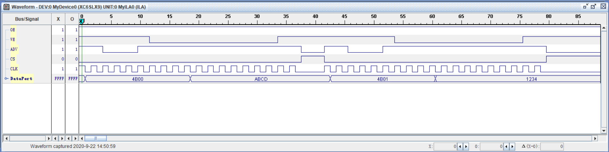
And when we read:

The data is already put on data/addr lines. However we get nothing from AM3358.
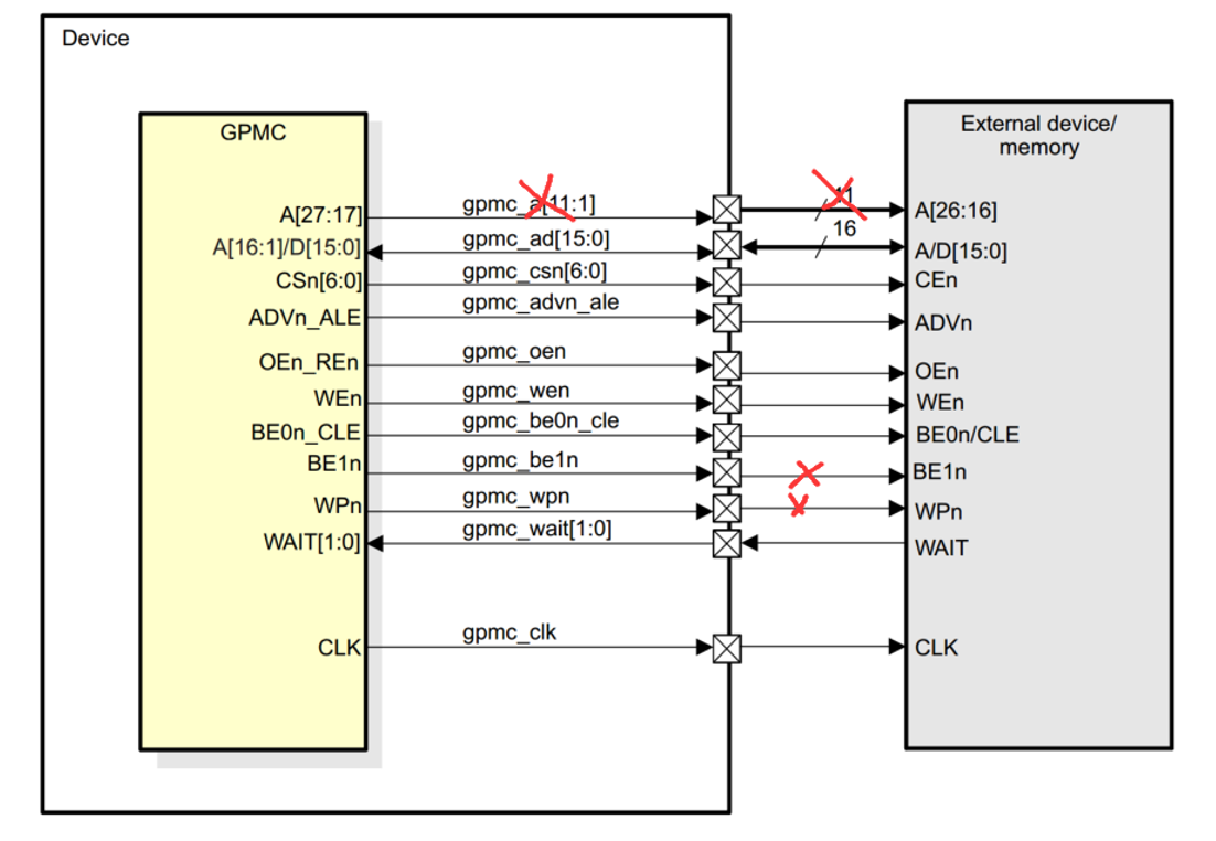
Our hardware scheme is:
We hope someone can give us some advise.
