This thread has been locked.

If you have a related question, please click the "Ask a related question" button in the top right corner. The newly created question will be automatically linked to this question.

CCS/AM3358: Processors forum

Part Number: AM3358

Tool/software: Code Composer Studio

Hi everyone,

I would like to have my PocketBeagle (AM3335 based, we can assume that it is BeagleBone board) connected to the Code Composer Studio via JTAG. I'm looking for some 'easy to reproduce' solution so I think there is only XDS100v3 and XDS110 possible. 

According to the  Debug Probe Performance Comparison XDS110 has significantly more throughput.

I have a MSP-EXP432P401R board with integrated XDS110 debugger which I would like to use. From XDS110 TI infopage PocketBeagle AM3335 processor is supported: 

Devices supported:
Sitara (AM335x, AM43xx, AM57xx, AM65xx, AMIC1xx)

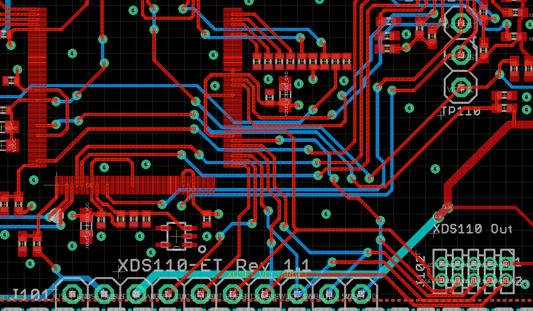
However, it corresponds to the XDS110 standalone debugger not an embedded version. When I looked at the XDS110 Embedded design on the MSP-EXP432P401R board I saw that XDS110 Out is connected directly to the TM4C1294NCPD TI Tiva microcontroller. This means that this embedded debugger does not support 1.8V JTAG protocol, which is used on Sitara processors like AM3358.

My question is: 

Could I still use this XDS110 Embedded version with PocketBeagle using some logic translator 3V3 <> 1V8 or there is sth more that should be included?

XDS100v3 includes additional CPLD which is among others used for logic level translation.

I will be really thankful for any useful information in advance.

  • Is you concern about the XDS110 not supporting 1.8V based on a board having it connected directly to a device that is operating at 3.3V? If so, that may not be correct.

    I'm not familiar with design details of the XDS110 debugger, but most debuggers have an IO supply detect signal which is used to select the IO voltage or simply power an internal level shifter.

    I went to the XDS110 link you inserted in your post and found the following comment which seems to indicate the XDS110 can support any IO voltage from 1.8V to 3.6V. So it doesn't appear you would need to insert any level-shifters in the path.

    The XDS110 family supports the traditional IEEE1149.1 (JTAG) as well as IEEE1149.7 (cJTAG) and ARM Serial Wire Debug (SWD)/Serial Wire Output (SWO) and operates with interface levels of +1.8V up to +3.6V.

    Regards,
    Paul


  • Thank you Paul for your response. 

    The statement "operates with interface levels of +1.8V up to +3.6V" is true only for full/standalone version of XDS110. I studied the hardware design of XDS110 embedded version (on the MSP-EXP432P401R board) and I'm sure that it will not support 1.8V level. There aren't any level logic translator or FPGA like on the XDS100. Instead there is a direct connection with Tiva processor (Main XDS110 IC) which operates on 3.3V.

    My real concern is... Is it enough to add logic level translator to the XDS110 embedded version and it will be able to operate with Sitara processor? I don't have a full version to verify it.

  • If this is the case, you will need to insert level-shifters.

    Level-shifters insert delays in each signal path which may require you to reduce your TCK operating frequency. 

    The IEEE 1149.1 specification requires JTAG output signals to change on the falling edge of TCK and JTAG input signals to be latched on the rising edge of TCK. Therefore, reducing the TCK operating frequency provides additional setup and hold time which allows you to compensate for the additional insertion delay.

    Regards,
    Paul