This thread has been locked.

If you have a related question, please click the "Ask a related question" button in the top right corner. The newly created question will be automatically linked to this question.

AM6548: cross domain SPI DMA

Part Number: AM6548
Other Parts Discussed in Thread: SYSBIOS,

Hello,

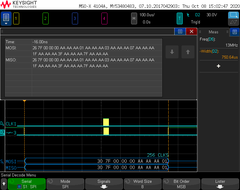
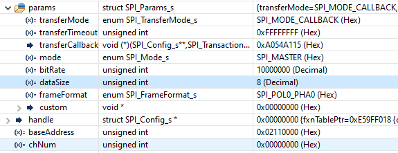
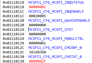
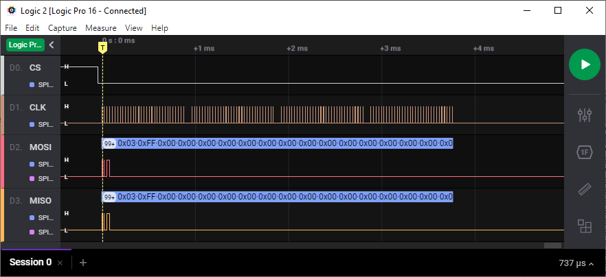
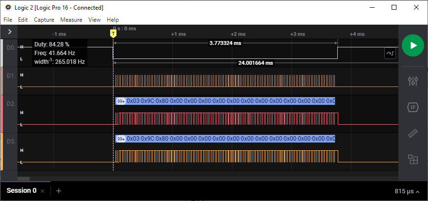
I am testing SPI of AM65X IDK in J20 connector. It is MCSPI1. My code is runing on R5F core and after a little hack  of the driver table I can send and receive.

I would like to test DMA and here is my question: is it possible to reach a peripheral  in MAIN domain by DMA from MCU domain?

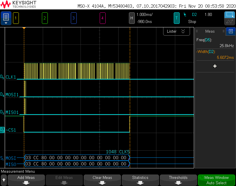
I have found pdk_jacinto_07_00_00\packages\ti\drv\spi\example\mcspi_slavemode\ example and was able to run it with success, but it deals with internally connected spi ports without domain crossing.

Regards,

Kalman

  • Kalman,

    There is no limitation of using MAIN domain UDMA/peripheral from MCU1_0.

    You need to tweak the SPI_soc.c to use MAIN domain McSPI peripheral and main domain McSPI PDMA threads

     #if defined (__aarch64__)

    #define SPI_PDMA_TX_THREAD_BASE        (CSL_PSILCFG_NAVSS_MAIN_PDMA_MAIN1_PSILD_THREAD_OFFSET + 0U)

    #define SPI_PDMA_RX_THREAD_BASE        (CSL_PSILCFG_NAVSS_MAIN_PDMA_MAIN1_PSILS_THREAD_OFFSET + 0U)

    #else

    #define SPI_PDMA_TX_THREAD_BASE        (CSL_PSILCFG_NAVSS_MCU_PDMA_MCU1_PSILD_THREAD_OFFSET + 0U)

    #define SPI_PDMA_RX_THREAD_BASE        (CSL_PSILCFG_NAVSS_MCU_PDMA_MCU1_PSILS_THREAD_OFFSET + 0U)

    Change this to

    #define SPI_PDMA_TX_THREAD_BASE        (CSL_PSILCFG_NAVSS_MAIN_PDMA_MAIN1_PSILD_THREAD_OFFSET + 0U)

    #define SPI_PDMA_RX_THREAD_BASE        (CSL_PSILCFG_NAVSS_MAIN_PDMA_MAIN1_PSILS_THREAD_OFFSET + 0U)

    #endif


    #if defined (__aarch64__)

            /* main domain */

            CSL_MCSPI0_CFG_BASE,                /* baseAddr */

            CSL_GIC0_INTR_MCSPI0_BUS_INTR_SPI,  /* intNum */

    #else

            /* mcu domain */

            CSL_MCU_MCSPI0_CFG_BASE,

            CSL_MCU0_INTR_MCSPI0_INTR_SPI,

    Change this to

            /* main domain */

            CSL_MCSPI0_CFG_BASE,                /* baseAddr */

            ??,  /* intNum */ 

    #endif

    For the intNum, from TRM,  MAIN2MCU_LVL_INTRTR0 router allows any 64 of 192 level interrupts from the MAIN voltage domain to be selected for routing to the MCU R5 Cores through MAIN2MCU_LVL_INTRTR0_MUXCNTL_y Register

    Table 9-64. MAIN2MCU_LVL_INTRTR0 Interrupt Map

    MAIN2MCU_INTRTR_LVL_IN_96 96 SPI_0_INT SPI0 interrupt Level

    I am trying to locate a reference code for you to program the interrupt routing through SYSFW.

    Regards,

    Garrett

  • Hi Garrett,

    thanks for good hint.

    I have made this hack in run time to reach MCSPI1 from R5F:

        /* add MCSPI1 to driver table */
        SPI_socGetInitCfg(2, &spi_cfg);
        spi_cfg.baseAddr = CSL_MCSPI1_CFG_BASE;
        SPI_socSetInitCfg(3, &spi_cfg);
    
        /* configure MCSPI1_CLK pin mux for reception, hack of pdk */
        HW_WR_REG32((CSL_CTRL_MMR0_CFG0_BASE + CSL_MAIN_CTRL_MMR_CFG0_PADCONFIG0 + MCU_SPI1_CLK_PADCFG_OFFSET), PIN_MODE(0) | \
                    ((PIN_PULL_DISABLE | PIN_INPUT_ENABLE) & (~PIN_PULL_DIRECTION)));


    Then I will try to add more details to the "hacked" entry according to your advice.

    Any very simple code example is welcome: I would like just to send and receive a buch of bytes at first and watch the signals by scope. I have  looped back MOSI to MISO pins of J20 connector by a jumper cap.

    Regards,

    Kalman

  • Kalman,

    Please refer to the attached files for MAIN2MCU Interrupt router for SPI function spiTestInteruptConfig().

    The interrupt number used by the SPI unit test is defined in the file intRtr_cfg.h.

    IntRtr_cfg.h

    /*
    *
    * Copyright (c) 2019 Texas Instruments Incorporated
    *
    * All rights reserved not granted herein.
    *
    * Limited License.
    *
    * Texas Instruments Incorporated grants a world-wide, royalty-free, non-exclusive
    * license under copyrights and patents it now or hereafter owns or controls to make,
    * have made, use, import, offer to sell and sell ("Utilize") this software subject to the
    * terms herein.  With respect to the foregoing patent license, such license is granted
    * solely to the extent that any such patent is necessary to Utilize the software alone.
    * The patent license shall not apply to any combinations which include this software,
    * other than combinations with devices manufactured by or for TI ("TI Devices").
    * No hardware patent is licensed hereunder.
    *
    * Redistributions must preserve existing copyright notices and reproduce this license
    * (including the above copyright notice and the disclaimer and (if applicable) source
    * code license limitations below) in the documentation and/or other materials provided
    * with the distribution
    *
    * Redistribution and use in binary form, without modification, are permitted provided
    * that the following conditions are met:
    *
    * *       No reverse engineering, decompilation, or disassembly of this software is
    * permitted with respect to any software provided in binary form.
    *
    * *       any redistribution and use are licensed by TI for use only with TI Devices.
    *
    * *       Nothing shall obligate TI to provide you with source code for the software
    * licensed and provided to you in object code.
    *
    * If software source code is provided to you, modification and redistribution of the
    * source code are permitted provided that the following conditions are met:
    *
    * *       any redistribution and use of the source code, including any resulting derivative
    * works, are licensed by TI for use only with TI Devices.
    *
    * *       any redistribution and use of any object code compiled from the source code
    * and any resulting derivative works, are licensed by TI for use only with TI Devices.
    *
    * Neither the name of Texas Instruments Incorporated nor the names of its suppliers
    *
    * may be used to endorse or promote products derived from this software without
    * specific prior written permission.
    *
    * DISCLAIMER.
    *
    * THIS SOFTWARE IS PROVIDED BY TI AND TI'S LICENSORS "AS IS" AND ANY EXPRESS
    * OR IMPLIED WARRANTIES, INCLUDING, BUT NOT LIMITED TO, THE IMPLIED WARRANTIES
    * OF MERCHANTABILITY AND FITNESS FOR A PARTICULAR PURPOSE ARE DISCLAIMED.
    * IN NO EVENT SHALL TI AND TI'S LICENSORS BE LIABLE FOR ANY DIRECT, INDIRECT,
    * INCIDENTAL, SPECIAL, EXEMPLARY, OR CONSEQUENTIAL DAMAGES (INCLUDING,
    * BUT NOT LIMITED TO, PROCUREMENT OF SUBSTITUTE GOODS OR SERVICES; LOSS OF USE,
    * DATA, OR PROFITS; OR BUSINESS INTERRUPTION) HOWEVER CAUSED AND ON ANY THEORY
    * OF LIABILITY, WHETHER IN CONTRACT, STRICT LIABILITY, OR TORT (INCLUDING NEGLIGENCE
    * OR OTHERWISE) ARISING IN ANY WAY OUT OF THE USE OF THIS SOFTWARE, EVEN IF ADVISED
    * OF THE POSSIBILITY OF SUCH DAMAGE.
    *
    */
    
    /**
     *  \file     spiTestApp.c
     *
     *  \brief    This file contains the SPI test application
     *
     */
    
    /* ========================================================================== */
    /*                             Include Files                                  */
    /* ========================================================================== */
    
    #include <string.h>
    #include "Std_Types.h"
    
    #include "testLib/spiTest.h"
    #include "IntRtr_Cfg.h"
    /* SCI Client */
    #include <ti/drv/sciclient/sciclient.h>
    
    /* Interrupt Registrations */
    #include <ti/osal/osal.h>
    
    /* ========================================================================== */
    /*                           Macros & Typedefs                                */
    /* ========================================================================== */
    
    #define ARRAYSIZE(x)                    (sizeof ((x)) / sizeof ((x)[0]))
    typedef void (*SpiApp_IsrType)(void);
    /**< ISR Type, used to store pointers to all ISR's */
    
    /* ========================================================================== */
    /*                         Structures and Enums                               */
    /* ========================================================================== */
    
    /* None */
    
    /* ========================================================================== */
    /*                          Function Declarations                             */
    /* ========================================================================== */
    static void SpiApp_platformInit(void);
    static void SpiApp_BuildIntrList(void);
    static void spiTestInterruptDeRegister(void);
    void SpiApp_SpiXIsr(uintptr_t SpiPtr);
    /* ========================================================================== */
    /*                            Global Variables                                */
    /* ========================================================================== */
    
    
    static volatile uint8   gSpiIntcCookie = 0U;
    static volatile uint32  gSpiIntcCheck = 0U;
    
    uint32 SpiApp_IntNumbers[SPI_MAX_HW_UNIT];
    /**< Stored the interrupt numbers for enabled all timers */
    uint32 SpiApp_RoutIntNumbers[SPI_MAX_HW_UNIT];
    /**< Flag to indicate if the timer is enabled or not */
    SpiApp_IsrType SpiApp_Isr[SPI_MAX_HW_UNIT];
    /**< Associated ISR */
    uint32 SpiApp_EnaInstance[SPI_MAX_HW_UNIT];
    /**< Flag to indicate if the timer is enabled or not */
    uint32 SpiApp_InstanceSrcId[SPI_MAX_HW_UNIT];
    /**< Store Module Device Id's used by SciClient for Interrupt Registration */
    HwiP_Handle	SpiApp_HwiHandle[SPI_MAX_HW_UNIT];
    /**< Store Hw Handle */
    /* ========================================================================== */
    /*                          Function Definitions                              */
    /* ========================================================================== */
    
    /**
     *  \file       trace.c
     *
     *  \brief      Trace implementation.
     *
     *              This abstracts and implements the definitions for
     *              user side traces statements and also details
     *              of variable traces supported in existing
     *              implementation.
     *
     */
    
    /* ========================================================================== */
    /*                             Include Files                                  */
    /* ========================================================================== */
    
    #include "Std_Types.h"
    #include "app_utils.h"
    
    /* ========================================================================== */
    /*                           Macros & Typedefs                                */
    /* ========================================================================== */
    
    
    /* ========================================================================== */
    /*                         Structure Declarations                             */
    /* ========================================================================== */
    
    /* None */
    
    /* ========================================================================== */
    /*                          Function Declarations                             */
    /* ========================================================================== */
    static void SpiApp_unlockMmrRegisters(uint32 lockKey0, uint32 lockKey1);
    
    /* ========================================================================== */
    /*                            Global Variables                                */
    /* ========================================================================== */
    
    /* None */
    
    /* ========================================================================== */
    /*                          Function Definitions                              */
    /* ========================================================================== */
    int main(void)
    {
        sint32 testPassed;
    
        SpiApp_platformInit();
        AppUtils_defaultInit();
    
        /* Invoke SPI test parser */
        testPassed = spiTestParser();
    
        /* Intc count should be zero - only enable called case */
        GT_assert(McalAppTrace, (0U == gSpiIntcCheck));
    
        GT_1trace(McalAppTrace, GT_INFO,
            " SPI Stack Usage: %d bytes\n", AppUtils_GetStackUsage());
        if (AppUtils_SpiCheckStackAndSectionCorruption() != E_OK)
        {
            testPassed = E_NOT_OK;
            GT_0trace(McalAppTrace, GT_ERR, " SPI Stack/section corruption!!!\n");
        }
    
        if (E_OK == testPassed)
        {
            GT_0trace(McalAppTrace, GT_INFO, " SPI Unit Test Passed!!!\n");
            AppUtils_LogResult(APP_UTILS_TEST_STATUS_PASS);
        }
        else
        {
            GT_0trace(McalAppTrace, GT_ERR, " SPI Unit Test Failed!!!\n");
            AppUtils_LogResult(APP_UTILS_TEST_STATUS_FAIL);
        }
    
    	/* De Initialize Interrupt Handle */
    	spiTestInterruptDeRegister();
    
        return (testPassed);
    }
    
    void SpiApp_MainDomainPinMux(uint32 offset, uint32 muxmode)
    {
        uint32 regVal = 0U;
    
        regVal = CSL_REG32_RD(CSL_CTRL_MMR0_CFG0_BASE + offset);
        regVal &= 0U;
        regVal |= muxmode;
        CSL_REG32_WR(CSL_CTRL_MMR0_CFG0_BASE + offset, regVal);
    
        return;
    }
    
    static void SpiApp_unlockMmrRegisters(uint32 lockKey0, uint32 lockKey1)
    {
        uint32 regVal = 0U;
    
        /* write Partition Lock Key 0 Register */
        CSL_REG32_WR(CSL_WKUP_CTRL_MMR0_CFG0_BASE + lockKey0, 0x68EF3490);
        /* write Partition Lock Key 1 Register */
        CSL_REG32_WR(CSL_WKUP_CTRL_MMR0_CFG0_BASE + lockKey1, 0xD172BC5A);
        /* Check for unlock */
        regVal = CSL_REG32_RD(CSL_WKUP_CTRL_MMR0_CFG0_BASE + lockKey0);
        while ((regVal & 0x1) != 0x1U)
        {
        }
    
        /* write Partition Lock Key 0 Register */
        CSL_REG32_WR(CSL_CTRL_MMR0_CFG0_BASE + lockKey0, 0x68EF3490);
        /* write Partition Lock Key 1 Register */
        CSL_REG32_WR(CSL_CTRL_MMR0_CFG0_BASE + lockKey1, 0xD172BC5A);
        /* Check for unlock */
        regVal = CSL_REG32_RD(CSL_CTRL_MMR0_CFG0_BASE + lockKey0);
        while ((regVal & 0x1) != 0x1U)
        {
        }
    
        return;
    }
    
    static void SpiApp_unlockMcuMmrRegisters(uint32 lockKey0, uint32 lockKey1)
    {
        uint32 regVal = 0U;
    
        /* write Partition Lock Key 0 Register */
        CSL_REG32_WR(CSL_MCU_CTRL_MMR0_CFG0_BASE + lockKey0, 0x68EF3490);
        /* write Partition Lock Key 1 Register */
        CSL_REG32_WR(CSL_MCU_CTRL_MMR0_CFG0_BASE + lockKey1, 0xD172BC5A);
        /* Check for unlock */
        regVal = CSL_REG32_RD(CSL_MCU_CTRL_MMR0_CFG0_BASE + lockKey0);
        while ((regVal & 0x1) != 0x1U)
        {
        }
    
        return;
    }
    
    #if defined (SOC_AM65XX) || defined (SOC_J721E) || defined (SOC_J7200)
    static void SpiApp_McuDomainPinMux(uint32 offset, uint32 muxmode)
    {
        uint32 regVal = 0U;
    
        regVal = CSL_REG32_RD(CSL_WKUP_CTRL_MMR0_CFG0_BASE + offset);
        regVal &= 0U;
        regVal |= muxmode;
        CSL_REG32_WR(CSL_WKUP_CTRL_MMR0_CFG0_BASE + offset, regVal);
    
        return;
    }
    #endif
    
    static void SpiApp_platformInit(void)
    {
    
        /* Unlock lock key registers for Partition : IO PAD
           configuration registers in MAIN_CTRL_MMR */
        /* write Partition 0 Register */
        SpiApp_unlockMmrRegisters(CSL_MAIN_CTRL_MMR_CFG0_LOCK0_KICK0, CSL_MAIN_CTRL_MMR_CFG0_LOCK0_KICK1);
        /* write Partition 1 Register */
        SpiApp_unlockMmrRegisters(CSL_MAIN_CTRL_MMR_CFG0_LOCK1_KICK0, CSL_MAIN_CTRL_MMR_CFG0_LOCK1_KICK1);
        /* write Partition 2 Register */
        SpiApp_unlockMmrRegisters(CSL_MAIN_CTRL_MMR_CFG0_LOCK2_KICK0, CSL_MAIN_CTRL_MMR_CFG0_LOCK2_KICK1);
        /* write Partition 3 Register */
        SpiApp_unlockMmrRegisters(CSL_MAIN_CTRL_MMR_CFG0_LOCK3_KICK0, CSL_MAIN_CTRL_MMR_CFG0_LOCK3_KICK1);
        /* write Partition 4 Register */
        SpiApp_unlockMmrRegisters(CSL_MAIN_CTRL_MMR_CFG0_LOCK4_KICK0, CSL_MAIN_CTRL_MMR_CFG0_LOCK4_KICK1);
    #if defined (SOC_J721E) || defined (SOC_AM65XX)
        /* write Partition 6 Register */
        SpiApp_unlockMmrRegisters(CSL_MAIN_CTRL_MMR_CFG0_LOCK6_KICK0, CSL_MAIN_CTRL_MMR_CFG0_LOCK6_KICK1);
    #endif
        /* write Partition 7 Register */
        SpiApp_unlockMmrRegisters(CSL_MAIN_CTRL_MMR_CFG0_LOCK7_KICK0, CSL_MAIN_CTRL_MMR_CFG0_LOCK7_KICK1);
    
        /* write Partition 0 Register */
        SpiApp_unlockMcuMmrRegisters(CSL_MCU_CTRL_MMR_CFG0_LOCK0_KICK0, CSL_MCU_CTRL_MMR_CFG0_LOCK0_KICK1);
        /* write Partition 1 Register */
        SpiApp_unlockMcuMmrRegisters(CSL_MCU_CTRL_MMR_CFG0_LOCK1_KICK0, CSL_MCU_CTRL_MMR_CFG0_LOCK1_KICK1);
        /* write Partition 2 Register */
        SpiApp_unlockMcuMmrRegisters(CSL_MCU_CTRL_MMR_CFG0_LOCK2_KICK0, CSL_MCU_CTRL_MMR_CFG0_LOCK2_KICK1);
    #if defined (SOC_AM65XX)
        /* write Partition 6 Register */
        SpiApp_unlockMcuMmrRegisters(CSL_MCU_CTRL_MMR_CFG0_LOCK6_KICK0, CSL_MCU_CTRL_MMR_CFG0_LOCK6_KICK1);
    #elif defined (SOC_J721E)
        /* write Partition 4 Register */
        SpiApp_unlockMcuMmrRegisters(CSL_MCU_CTRL_MMR_CFG0_LOCK4_KICK0, CSL_MCU_CTRL_MMR_CFG0_LOCK4_KICK1);
    #endif
        /* Enable MCU_MCSPI1 and MCSPI3 independently pin out */
        CSL_REG32_WR(CSL_MCU_CTRL_MMR0_CFG0_BASE + CSL_MCU_CTRL_MMR_CFG0_MCU_SPI1_CTRL, CSL_MCU_CTRL_MMR_CFG0_MCU_SPI1_CTRL_SPI1_LINKDIS_MASK);
    
    #if defined (SOC_AM65XX)
        /* MCU MCSPI 0 CS0 PAD configuration */
        SpiApp_McuDomainPinMux(CSL_WKUP_CTRL_MMR_CFG0_PADCONFIG39, 0x40000U);
    
        /* MCU MCSPI 0 CS1 PAD configuration */
        SpiApp_McuDomainPinMux(CSL_WKUP_CTRL_MMR_CFG0_PADCONFIG19, 0x40005U);
    
        /*  MCU MCSPI 0 CS2 PAD configuration */
        SpiApp_McuDomainPinMux(CSL_WKUP_CTRL_MMR_CFG0_PADCONFIG21, 0x40005U);
    
        /*  MCU MCSPI 0 CS3 PAD configuration */
        SpiApp_McuDomainPinMux(CSL_WKUP_CTRL_MMR_CFG0_PADCONFIG48, 0x40002U);
    
        /* MCU MCSPI 0 D1 PAD configuration */
        SpiApp_McuDomainPinMux(CSL_WKUP_CTRL_MMR_CFG0_PADCONFIG38, 0x40000U);
    
        /* MCU MCSPI 0 D0 PAD configuration */
        SpiApp_McuDomainPinMux(CSL_WKUP_CTRL_MMR_CFG0_PADCONFIG37, 0x40000U);
    
        /* MCU MCSPI 0 CLK PAD configuration */
        SpiApp_McuDomainPinMux(CSL_WKUP_CTRL_MMR_CFG0_PADCONFIG36, 0x40000U);
    
        /* MCU MCSPI 1 CS0 PAD configuration */
        SpiApp_McuDomainPinMux(CSL_WKUP_CTRL_MMR_CFG0_PADCONFIG1, 0x40001U);
    
        /* MCU MCSPI 1 CS1 PAD configuration */
        SpiApp_McuDomainPinMux(CSL_WKUP_CTRL_MMR_CFG0_PADCONFIG17, 0x40005U);
    
        /*  MCU MCSPI 1 CS2 PAD configuration */
        SpiApp_McuDomainPinMux(CSL_WKUP_CTRL_MMR_CFG0_PADCONFIG18, 0x40005U);
    
        /*  MCU MCSPI 1 CS3 PAD configuration */
        SpiApp_McuDomainPinMux(CSL_WKUP_CTRL_MMR_CFG0_PADCONFIG3, 0x40002U);
    
        /* MCU MCSPI 1 D1 PAD configuration */
        SpiApp_McuDomainPinMux(CSL_WKUP_CTRL_MMR_CFG0_PADCONFIG46, 0x40001U);
    
        /* MCU MCSPI 1 D0 PAD configuration */
        SpiApp_McuDomainPinMux(CSL_WKUP_CTRL_MMR_CFG0_PADCONFIG45, 0x40001U);
    
        /* MCU MCSPI 1 CLK PAD configuration */
        SpiApp_McuDomainPinMux(CSL_WKUP_CTRL_MMR_CFG0_PADCONFIG44, 0x40001U);
    
        /* MCSPI 0 CS0 PAD configuration */
        SpiApp_MainDomainPinMux(CSL_MAIN_CTRL_MMR_CFG0_PADCONFIG111, 0x40000U);
    
        /* MCSPI 0 CS1 PAD configuration */
        SpiApp_MainDomainPinMux(CSL_MAIN_CTRL_MMR_CFG0_PADCONFIG112, 0x40000U);
    
        /*  MCSPI 0 CS2 PAD configuration */
        SpiApp_MainDomainPinMux(CSL_MAIN_CTRL_MMR_CFG0_PADCONFIG123, 0x40002U);
    
        /*  MCSPI 0 CS3 PAD configuration */
        SpiApp_MainDomainPinMux(CSL_MAIN_CTRL_MMR_CFG0_PADCONFIG124, 0x40002U);
    
        /* MCSPI 0 D1 PAD configuration */
        SpiApp_MainDomainPinMux(CSL_MAIN_CTRL_MMR_CFG0_PADCONFIG115, 0x40000U);
    
        /* MCSPI 0 D0 PAD configuration */
        SpiApp_MainDomainPinMux(CSL_MAIN_CTRL_MMR_CFG0_PADCONFIG114, 0x40000U);
    
        /* MCSPI 0 CLK PAD configuration */
        SpiApp_MainDomainPinMux(CSL_MAIN_CTRL_MMR_CFG0_PADCONFIG113, 0x40000U);
    
        /* MCSPI 1 CS0 PAD configuration */
        SpiApp_MainDomainPinMux(CSL_MAIN_CTRL_MMR_CFG0_PADCONFIG116, 0x40000U);
    
        /* MCSPI 1 CS1 PAD configuration */
        SpiApp_MainDomainPinMux(CSL_MAIN_CTRL_MMR_CFG0_PADCONFIG117, 0x40000U);
    
        /*  MCSPI 1 CS2 PAD configuration */
        SpiApp_MainDomainPinMux(CSL_MAIN_CTRL_MMR_CFG0_PADCONFIG96, 0x40001U);
    
        /*  MCSPI 1 CS3 PAD configuration */
        SpiApp_MainDomainPinMux(CSL_MAIN_CTRL_MMR_CFG0_PADCONFIG97, 0x40001U);
    
        /* MCSPI 1 D1 PAD configuration */
        SpiApp_MainDomainPinMux(CSL_MAIN_CTRL_MMR_CFG0_PADCONFIG120, 0x40000U);
    
        /* MCSPI 1 D0 PAD configuration */
        SpiApp_MainDomainPinMux(CSL_MAIN_CTRL_MMR_CFG0_PADCONFIG119, 0x40000U);
    
        /* MCSPI 1 CLK PAD configuration */
        SpiApp_MainDomainPinMux(CSL_MAIN_CTRL_MMR_CFG0_PADCONFIG118, 0x40000U);
    
        /* MCSPI 2 CS0 PAD configuration */
        SpiApp_MainDomainPinMux(CSL_MAIN_CTRL_MMR_CFG0_PADCONFIG83, 0x40004U);
    
        /* MCSPI 2 CS1 PAD configuration */
        SpiApp_MainDomainPinMux(CSL_MAIN_CTRL_MMR_CFG0_PADCONFIG65, 0x40004U);
    
        /*  MCSPI 2 CS2 PAD configuration */
        SpiApp_MainDomainPinMux(CSL_MAIN_CTRL_MMR_CFG0_PADCONFIG66, 0x40004U);
    
        /*  MCSPI 2 CS3 PAD configuration */
        SpiApp_MainDomainPinMux(CSL_MAIN_CTRL_MMR_CFG0_PADCONFIG86, 0x40004U);
    
        /* MCSPI 2 D1 PAD configuration */
        SpiApp_MainDomainPinMux(CSL_MAIN_CTRL_MMR_CFG0_PADCONFIG95, 0x40004U);
    
        /* MCSPI 2 D0 PAD configuration */
        SpiApp_MainDomainPinMux(CSL_MAIN_CTRL_MMR_CFG0_PADCONFIG94, 0x40004U);
    
        /* MCSPI 2 CLK PAD configuration */
        SpiApp_MainDomainPinMux(CSL_MAIN_CTRL_MMR_CFG0_PADCONFIG93, 0x40004U);
    
        /* MCSPI 3 CS0 PAD configuration */
        SpiApp_MainDomainPinMux(CSL_MAIN_CTRL_MMR_CFG0_PADCONFIG152, 0x40004U);
    
        /* MCSPI 3 CS1 PAD configuration */
        SpiApp_MainDomainPinMux(CSL_MAIN_CTRL_MMR_CFG0_PADCONFIG134, 0x40004U);
    
        /*  MCSPI 3 CS2 PAD configuration */
        SpiApp_MainDomainPinMux(CSL_MAIN_CTRL_MMR_CFG0_PADCONFIG135, 0x40004U);
    
        /*  MCSPI 3 CS3 PAD configuration */
        SpiApp_MainDomainPinMux(CSL_MAIN_CTRL_MMR_CFG0_PADCONFIG154, 0x40004U);
    
        /* MCSPI 3 D1 PAD configuration */
        SpiApp_MainDomainPinMux(CSL_MAIN_CTRL_MMR_CFG0_PADCONFIG164, 0x40004U);
    
        /* MCSPI 3 D0 PAD configuration */
        SpiApp_MainDomainPinMux(CSL_MAIN_CTRL_MMR_CFG0_PADCONFIG163, 0x40004U);
    
        /* MCSPI 3 CLK PAD configuration */
        SpiApp_MainDomainPinMux(CSL_MAIN_CTRL_MMR_CFG0_PADCONFIG162, 0x40004U);
    #elif defined (SOC_J721E)
        /* MCU MCSPI 0 CS0 PAD configuration */
        SpiApp_McuDomainPinMux(CSL_WKUP_CTRL_MMR_CFG0_PADCONFIG39, 0x40000U);
    
        /* MCU MCSPI 0 CS1 PAD configuration */
        SpiApp_McuDomainPinMux(CSL_WKUP_CTRL_MMR_CFG0_PADCONFIG19, 0x40005U);
    
        /*  MCU MCSPI 0 CS2 PAD configuration */
        SpiApp_McuDomainPinMux(CSL_WKUP_CTRL_MMR_CFG0_PADCONFIG21, 0x40005U);
    
        /*  MCU MCSPI 0 CS3 PAD configuration */
        SpiApp_McuDomainPinMux(CSL_WKUP_CTRL_MMR_CFG0_PADCONFIG48, 0x40002U);
    
        /* MCU MCSPI 0 D1 PAD configuration */
        SpiApp_McuDomainPinMux(CSL_WKUP_CTRL_MMR_CFG0_PADCONFIG38, 0x40000U);
    
        /* MCU MCSPI 0 D0 PAD configuration */
        SpiApp_McuDomainPinMux(CSL_WKUP_CTRL_MMR_CFG0_PADCONFIG37, 0x40000U);
    
        /* MCU MCSPI 0 CLK PAD configuration */
        SpiApp_McuDomainPinMux(CSL_WKUP_CTRL_MMR_CFG0_PADCONFIG36, 0x40000U);
    
        /* MCU MCSPI 1 CS0 PAD configuration */
        SpiApp_McuDomainPinMux(CSL_WKUP_CTRL_MMR_CFG0_PADCONFIG47, 0x40001U);
    
        /* MCU MCSPI 1 CS1 PAD configuration */
        SpiApp_McuDomainPinMux(CSL_WKUP_CTRL_MMR_CFG0_PADCONFIG57, 0x40005U);
    
        /*  MCU MCSPI 1 CS2 PAD configuration */
        SpiApp_McuDomainPinMux(CSL_WKUP_CTRL_MMR_CFG0_PADCONFIG59, 0x40005U);
    
        /*  MCU MCSPI 1 CS3 PAD configuration */
        SpiApp_McuDomainPinMux(CSL_WKUP_CTRL_MMR_CFG0_PADCONFIG49, 0x40002U);
    
        /* MCU MCSPI 1 D1 PAD configuration */
        SpiApp_McuDomainPinMux(CSL_WKUP_CTRL_MMR_CFG0_PADCONFIG46, 0x40001U);
    
        /* MCU MCSPI 1 D0 PAD configuration */
        SpiApp_McuDomainPinMux(CSL_WKUP_CTRL_MMR_CFG0_PADCONFIG45, 0x40001U);
    
        /* MCU MCSPI 1 CLK PAD configuration */
        SpiApp_McuDomainPinMux(CSL_WKUP_CTRL_MMR_CFG0_PADCONFIG44, 0x40001U);
    
        /* MCSPI 0 CS0 PAD configuration */
        SpiApp_MainDomainPinMux(CSL_MAIN_CTRL_MMR_CFG0_PADCONFIG112, 0x40000U);
    
        /* MCSPI 0 CS1 PAD configuration */
        SpiApp_MainDomainPinMux(CSL_MAIN_CTRL_MMR_CFG0_PADCONFIG113, 0x40000U);
    
        /*  MCSPI 0 CS2 PAD configuration */
        SpiApp_MainDomainPinMux(CSL_MAIN_CTRL_MMR_CFG0_PADCONFIG124, 0x40002U);
    
        /*  MCSPI 0 CS3 PAD configuration */
        SpiApp_MainDomainPinMux(CSL_MAIN_CTRL_MMR_CFG0_PADCONFIG125, 0x40002U);
    
        /* MCSPI 0 D1 PAD configuration */
        SpiApp_MainDomainPinMux(CSL_MAIN_CTRL_MMR_CFG0_PADCONFIG116, 0x40000U);
    
        /* MCSPI 0 D0 PAD configuration */
        SpiApp_MainDomainPinMux(CSL_MAIN_CTRL_MMR_CFG0_PADCONFIG115, 0x40000U);
    
        /* MCSPI 0 CLK PAD configuration */
        SpiApp_MainDomainPinMux(CSL_MAIN_CTRL_MMR_CFG0_PADCONFIG114, 0x40000U);
    
        /* MCSPI 1 CS0 PAD configuration */
        SpiApp_MainDomainPinMux(CSL_MAIN_CTRL_MMR_CFG0_PADCONFIG117, 0x40000U);
    
        /* MCSPI 1 CS1 PAD configuration */
        SpiApp_MainDomainPinMux(CSL_MAIN_CTRL_MMR_CFG0_PADCONFIG118, 0x40000U);
    
        /*  MCSPI 1 CS2 PAD configuration */
        SpiApp_MainDomainPinMux(CSL_MAIN_CTRL_MMR_CFG0_PADCONFIG42, 0x40001U);
    
        /*  MCSPI 1 CS3 PAD configuration */
        SpiApp_MainDomainPinMux(CSL_MAIN_CTRL_MMR_CFG0_PADCONFIG43, 0x40001U);
    
        /* MCSPI 1 D1 PAD configuration */
        SpiApp_MainDomainPinMux(CSL_MAIN_CTRL_MMR_CFG0_PADCONFIG121, 0x40000U);
    
        /* MCSPI 1 D0 PAD configuration */
        SpiApp_MainDomainPinMux(CSL_MAIN_CTRL_MMR_CFG0_PADCONFIG120, 0x40000U);
    
        /* MCSPI 1 CLK PAD configuration */
        SpiApp_MainDomainPinMux(CSL_MAIN_CTRL_MMR_CFG0_PADCONFIG119, 0x40000U);
    
        /* MCSPI 2 CS0 PAD configuration */
        SpiApp_MainDomainPinMux(CSL_MAIN_CTRL_MMR_CFG0_PADCONFIG124, 0x40004U);
    
        /* MCSPI 2 CS1 PAD configuration */
        SpiApp_MainDomainPinMux(CSL_MAIN_CTRL_MMR_CFG0_PADCONFIG122, 0x40004U);
    
        /*  MCSPI 2 CS2 PAD configuration */
        SpiApp_MainDomainPinMux(CSL_MAIN_CTRL_MMR_CFG0_PADCONFIG123, 0x40004U);
    
        /*  MCSPI 2 CS3 PAD configuration */
        SpiApp_MainDomainPinMux(CSL_MAIN_CTRL_MMR_CFG0_PADCONFIG140, 0x40004U);
    
        /* MCSPI 2 D1 PAD configuration */
        SpiApp_MainDomainPinMux(CSL_MAIN_CTRL_MMR_CFG0_PADCONFIG128, 0x40004U);
    
        /* MCSPI 2 D0 PAD configuration */
        SpiApp_MainDomainPinMux(CSL_MAIN_CTRL_MMR_CFG0_PADCONFIG129, 0x40004U);
    
        /* MCSPI 2 CLK PAD configuration */
        SpiApp_MainDomainPinMux(CSL_MAIN_CTRL_MMR_CFG0_PADCONFIG125, 0x40004U);
    
        /* MCSPI 3 CS0 PAD configuration */
        SpiApp_MainDomainPinMux(CSL_MAIN_CTRL_MMR_CFG0_PADCONFIG71, 0x40004U);
    
        /* MCSPI 3 CS1 PAD configuration */
        SpiApp_MainDomainPinMux(CSL_MAIN_CTRL_MMR_CFG0_PADCONFIG53, 0x40004U);
    
        /*  MCSPI 3 CS2 PAD configuration */
        SpiApp_MainDomainPinMux(CSL_MAIN_CTRL_MMR_CFG0_PADCONFIG54, 0x40004U);
    
        /*  MCSPI 3 CS3 PAD configuration */
        SpiApp_MainDomainPinMux(CSL_MAIN_CTRL_MMR_CFG0_PADCONFIG73, 0x40004U);
    
        /* MCSPI 3 D1 PAD configuration */
        SpiApp_MainDomainPinMux(CSL_MAIN_CTRL_MMR_CFG0_PADCONFIG83, 0x40004U);
    
        /* MCSPI 3 D0 PAD configuration */
        SpiApp_MainDomainPinMux(CSL_MAIN_CTRL_MMR_CFG0_PADCONFIG82, 0x40004U);
    
        /* MCSPI 3 CLK PAD configuration */
        SpiApp_MainDomainPinMux(CSL_MAIN_CTRL_MMR_CFG0_PADCONFIG81, 0x40004U);
    
        /* MCSPI 5 CS0 PAD configuration */
        SpiApp_MainDomainPinMux(CSL_MAIN_CTRL_MMR_CFG0_PADCONFIG103, 0x40003U);
    
        /* MCSPI 5 CS1 PAD configuration */
        SpiApp_MainDomainPinMux(CSL_MAIN_CTRL_MMR_CFG0_PADCONFIG109, 0x40003U);
    
        /*  MCSPI 5 CS2 PAD configuration */
        SpiApp_MainDomainPinMux(CSL_MAIN_CTRL_MMR_CFG0_PADCONFIG101, 0x40003U);
    
        /*  MCSPI 5 CS3 PAD configuration */
        SpiApp_MainDomainPinMux(CSL_MAIN_CTRL_MMR_CFG0_PADCONFIG100, 0x40003U);
    
        /* MCSPI 5 D1 PAD configuration */
        SpiApp_MainDomainPinMux(CSL_MAIN_CTRL_MMR_CFG0_PADCONFIG108, 0x40003U);
    
        /* MCSPI 5 D0 PAD configuration */
        SpiApp_MainDomainPinMux(CSL_MAIN_CTRL_MMR_CFG0_PADCONFIG102, 0x40003U);
    
        /* MCSPI 5 CLK PAD configuration */
        SpiApp_MainDomainPinMux(CSL_MAIN_CTRL_MMR_CFG0_PADCONFIG104, 0x40003U);
    
        /* MCSPI 6 CS0 PAD configuration */
        SpiApp_MainDomainPinMux(CSL_MAIN_CTRL_MMR_CFG0_PADCONFIG29, 0x40004U);
    
        /* MCSPI 6 CS1 PAD configuration */
        SpiApp_MainDomainPinMux(CSL_MAIN_CTRL_MMR_CFG0_PADCONFIG10, 0x40004U);
    
        /*  MCSPI 6 CS2 PAD configuration */
        SpiApp_MainDomainPinMux(CSL_MAIN_CTRL_MMR_CFG0_PADCONFIG11, 0x40004U);
    
        /*  MCSPI 6 CS3 PAD configuration */
        SpiApp_MainDomainPinMux(CSL_MAIN_CTRL_MMR_CFG0_PADCONFIG31, 0x40004U);
    
        /* MCSPI 6 D1 PAD configuration */
        SpiApp_MainDomainPinMux(CSL_MAIN_CTRL_MMR_CFG0_PADCONFIG41, 0x40004U);
    
        /* MCSPI 6 D0 PAD configuration */
        SpiApp_MainDomainPinMux(CSL_MAIN_CTRL_MMR_CFG0_PADCONFIG40, 0x40004U);
    
        /* MCSPI 6 CLK PAD configuration */
        SpiApp_MainDomainPinMux(CSL_MAIN_CTRL_MMR_CFG0_PADCONFIG39, 0x40004U);
    
    #elif defined (SOC_J7200)
        /* MCU MCSPI 0 CS0 PAD configuration */
        SpiApp_McuDomainPinMux(CSL_WKUP_CTRL_MMR_CFG0_PADCONFIG43, 0x40000U);
    
        /* MCU MCSPI 0 D1 PAD configuration */
        SpiApp_McuDomainPinMux(CSL_WKUP_CTRL_MMR_CFG0_PADCONFIG42, 0x40000U);
    
        /* MCU MCSPI 0 D0 PAD configuration */
        SpiApp_McuDomainPinMux(CSL_WKUP_CTRL_MMR_CFG0_PADCONFIG41, 0x40000U);
    
        /* MCU MCSPI 0 CLK PAD configuration */
        SpiApp_McuDomainPinMux(CSL_WKUP_CTRL_MMR_CFG0_PADCONFIG40, 0x40000U);
    
        /* MCU MCSPI 1 CS0 PAD configuration */
        SpiApp_McuDomainPinMux(CSL_WKUP_CTRL_MMR_CFG0_PADCONFIG51, 0x40001U);
    
        /* MCU MCSPI 1 D1 PAD configuration */
        SpiApp_McuDomainPinMux(CSL_WKUP_CTRL_MMR_CFG0_PADCONFIG50, 0x40001U);
    
        /* MCU MCSPI 1 D0 PAD configuration */
        SpiApp_McuDomainPinMux(CSL_WKUP_CTRL_MMR_CFG0_PADCONFIG49, 0x40001U);
    
        /* MCU MCSPI 1 CLK PAD configuration */
        SpiApp_McuDomainPinMux(CSL_WKUP_CTRL_MMR_CFG0_PADCONFIG48, 0x40001U);
    
        /* MCSPI 0 CS0 PAD configuration */
        SpiApp_MainDomainPinMux(CSL_MAIN_CTRL_MMR_CFG0_PADCONFIG48, 0x40000U);
    
        /* MCSPI 0 D1 PAD configuration */
        SpiApp_MainDomainPinMux(CSL_MAIN_CTRL_MMR_CFG0_PADCONFIG52, 0x40000U);
    
        /* MCSPI 0 D0 PAD configuration */
        SpiApp_MainDomainPinMux(CSL_MAIN_CTRL_MMR_CFG0_PADCONFIG51, 0x40000U);
    
        /* MCSPI 0 CLK PAD configuration */
        SpiApp_MainDomainPinMux(CSL_MAIN_CTRL_MMR_CFG0_PADCONFIG50, 0x40000U);
    
        /* MCSPI 1 CS0 PAD configuration */
        SpiApp_MainDomainPinMux(CSL_MAIN_CTRL_MMR_CFG0_PADCONFIG59, 0x40008U);
    
        /* MCSPI 1 D1 PAD configuration */
        SpiApp_MainDomainPinMux(CSL_MAIN_CTRL_MMR_CFG0_PADCONFIG65, 0x40008U);
    
        /* MCSPI 1 D0 PAD configuration */
        SpiApp_MainDomainPinMux(CSL_MAIN_CTRL_MMR_CFG0_PADCONFIG62, 0x40008U);
    
        /* MCSPI 1 CLK PAD configuration */
        SpiApp_MainDomainPinMux(CSL_MAIN_CTRL_MMR_CFG0_PADCONFIG64, 0x40008U);
    
        /* MCSPI 2 CS0 PAD configuration */
        SpiApp_MainDomainPinMux(CSL_MAIN_CTRL_MMR_CFG0_PADCONFIG30, 0x40008U);
    
        /* MCSPI 2 D1 PAD configuration */
        SpiApp_MainDomainPinMux(CSL_MAIN_CTRL_MMR_CFG0_PADCONFIG35, 0x40008U);
    
        /* MCSPI 2 D0 PAD configuration */
        SpiApp_MainDomainPinMux(CSL_MAIN_CTRL_MMR_CFG0_PADCONFIG34, 0x40008U);
    
        /* MCSPI 2 CLK PAD configuration */
        SpiApp_MainDomainPinMux(CSL_MAIN_CTRL_MMR_CFG0_PADCONFIG29, 0x40008U);
    
        /* MCSPI 3 CS0 PAD configuration */
        SpiApp_MainDomainPinMux(CSL_MAIN_CTRL_MMR_CFG0_PADCONFIG22, 0x40008U);
    
        /* MCSPI 3 D1 PAD configuration */
        SpiApp_MainDomainPinMux(CSL_MAIN_CTRL_MMR_CFG0_PADCONFIG28, 0x40008U);
    
        /* MCSPI 3 D0 PAD configuration */
        SpiApp_MainDomainPinMux(CSL_MAIN_CTRL_MMR_CFG0_PADCONFIG27, 0x40008U);
    
        /* MCSPI 3 CLK PAD configuration */
        SpiApp_MainDomainPinMux(CSL_MAIN_CTRL_MMR_CFG0_PADCONFIG26, 0x40008U);
    
        /* MCSPI 5 CS0 PAD configuration */
        SpiApp_MainDomainPinMux(CSL_MAIN_CTRL_MMR_CFG0_PADCONFIG15, 0x40008U);
    
        /* MCSPI 5 D1 PAD configuration */
        SpiApp_MainDomainPinMux(CSL_MAIN_CTRL_MMR_CFG0_PADCONFIG17, 0x40008U);
    
        /* MCSPI 5 D0 PAD configuration */
        SpiApp_MainDomainPinMux(CSL_MAIN_CTRL_MMR_CFG0_PADCONFIG14, 0x40008U);
    
        /* MCSPI 5 CLK PAD configuration */
        SpiApp_MainDomainPinMux(CSL_MAIN_CTRL_MMR_CFG0_PADCONFIG16, 0x40008U);
    
        /* MCSPI 6 CS0 PAD configuration */
        SpiApp_MainDomainPinMux(CSL_MAIN_CTRL_MMR_CFG0_PADCONFIG10, 0x40008U);
    
        /* MCSPI 6 D1 PAD configuration */
        SpiApp_MainDomainPinMux(CSL_MAIN_CTRL_MMR_CFG0_PADCONFIG40, 0x40008U);
    
        /* MCSPI 6 D0 PAD configuration */
        SpiApp_MainDomainPinMux(CSL_MAIN_CTRL_MMR_CFG0_PADCONFIG39, 0x40008U);
    
        /* MCSPI 6 CLK PAD configuration */
        SpiApp_MainDomainPinMux(CSL_MAIN_CTRL_MMR_CFG0_PADCONFIG38, 0x40008U);
    
        /* MCSPI 7 CS0 PAD configuration */
        SpiApp_MainDomainPinMux(CSL_MAIN_CTRL_MMR_CFG0_PADCONFIG55, 0x40006U);
    
        /* MCSPI 7 D1 PAD configuration */
        SpiApp_MainDomainPinMux(CSL_MAIN_CTRL_MMR_CFG0_PADCONFIG58, 0x40006U);
    
        /* MCSPI 7 D0 PAD configuration */
        SpiApp_MainDomainPinMux(CSL_MAIN_CTRL_MMR_CFG0_PADCONFIG57, 0x40006U);
    
        /* MCSPI 7 CLK PAD configuration */
        SpiApp_MainDomainPinMux(CSL_MAIN_CTRL_MMR_CFG0_PADCONFIG56, 0x40006U);
    
    #endif
    
        /* Build Intr List */
    	SpiApp_BuildIntrList();
        /* Configure interrupts for MCSPI */
        spiTestInterruptConfig();
        /* Initialize memory ections  */
    	AppUtils_SpiSectionInit();
    
        return;
    
    }
    
    void spiTestInterruptConfig(void)
    {
        uint32 idx;
        struct tisci_msg_rm_irq_set_req     rmIrqReq;
        struct tisci_msg_rm_irq_set_resp    rmIrqResp;
        Int32 retVal;
        OsalRegisterIntrParams_t    intrPrms;
        OsalInterruptRetCode_e      osalRetVal;
        HwiP_Handle hwiHandle;
        Intc_Init();    /* Interrupt handler initialized, here as other functions
                         * can use API's to clear pending interrupts if any
                         */
    
        for (idx = 0U; idx < SPI_MAX_HW_UNIT; idx++)
        {
            if (0U != SpiApp_EnaInstance[idx])
            {
                if ((APP_SPI_MCU_0_INT != SpiApp_IntNumbers[idx]) &&
                     (APP_SPI_MCU_1_INT != SpiApp_IntNumbers[idx]) &&
                     (APP_SPI_MCU_2_INT != SpiApp_IntNumbers[idx]))
                {
                    /* We will have to use the routed interrupt number
                        subsequently */
                    SpiApp_IntNumbers[idx] = SpiApp_RoutIntNumbers[idx];
    
                    /* If the timer is not in MCU domain, the interrupt router will
                        have to be configured */
                    /* Set the destination interrupt */
                    rmIrqReq.valid_params           = TISCI_MSG_VALUE_RM_DST_ID_VALID;
                    rmIrqReq.valid_params          |= TISCI_MSG_VALUE_RM_DST_HOST_IRQ_VALID;
                    rmIrqReq.src_id                 = SpiApp_InstanceSrcId[idx];
                    rmIrqReq.global_event           = 0U;
                    rmIrqReq.src_index              = 0U;
    #if defined (SOC_AM65XX)
                    rmIrqReq.dst_id                 = TISCI_DEV_MCU_ARMSS0_CPU0;
    #elif defined (SOC_J721E) || defined (SOC_J7200)
                    rmIrqReq.dst_id                 = TISCI_DEV_MCU_R5FSS0_CORE0;
    #endif
                    rmIrqReq.dst_host_irq           = SpiApp_RoutIntNumbers[idx];
                    rmIrqReq.ia_id                  = 0U;
                    rmIrqReq.vint                   = 0U;
                    rmIrqReq.vint_status_bit_index  = 0U;
                    rmIrqReq.secondary_host         = TISCI_MSG_VALUE_RM_UNUSED_SECONDARY_HOST;
                    retVal = Sciclient_rmIrqSet(
                                 &rmIrqReq, &rmIrqResp, APP_SCICLIENT_TIMEOUT);
                    if(CSL_PASS != retVal)
                    {
                        GT_0trace(McalAppTrace, GT_ERR,
                            "Error in SciClient Interrupt Params Configuration!!!\n");
                    }
                }
    			Osal_RegisterInterrupt_initParams(&intrPrms);
    			intrPrms.corepacConfig.arg          = (uintptr_t)SpiApp_Isr[idx];
    			intrPrms.corepacConfig.isrRoutine   = &SpiApp_SpiXIsr;
    			intrPrms.corepacConfig.priority     = 1U;
    			intrPrms.corepacConfig.corepacEventNum = 0U; /* NOT USED ? */
    			intrPrms.corepacConfig.intVecNum        = SpiApp_IntNumbers[idx];
    
    			osalRetVal = Osal_RegisterInterrupt(&intrPrms, &hwiHandle);
    			if(OSAL_INT_SUCCESS != osalRetVal)
    			{
    				AppUtils_printf(APP_UTILS_PRINT_MSG_NORMAL,
    								  ": Error %d !!!\n");
    			}
    			SpiApp_HwiHandle[idx] = hwiHandle;
            }
    		
        }
        return;
    }
    
    static void spiTestInterruptDeRegister(void)
    {
    	uint32 idx;
        for (idx = 0U; idx < SPI_MAX_HW_UNIT; idx++)
        {
    		Osal_DeleteInterrupt(SpiApp_HwiHandle[idx], 0U);
    	}
    }
    
    static void SpiApp_BuildIntrList(void)
    {
        uint32 idx, flag, intNum, routIntNum, timerDevId;
        SpiApp_IsrType pIsrHandler = NULL;
    
        for (idx = 0U; idx < SPI_MAX_HW_UNIT; idx++)
        {
            SpiApp_EnaInstance[idx] = 0U;
            SpiApp_IntNumbers[idx] = 0U;
            SpiApp_InstanceSrcId[idx] = 0U;
        }
        /*
         * Build isr and interrupt number for all timers
         */
        for (idx = 0U; idx < SPI_MAX_HW_UNIT; idx++)
        {
            flag = 0U;
            routIntNum = 0U;
    		timerDevId = 0U;
            switch(idx)
            {
                case SPI_UNIT_MCU_MCSPI0:
                    intNum = APP_SPI_MCU_0_INT;
    #if (STD_ON == SPI_UNIT_MCU_MCSPI0_ACTIVE)
                    pIsrHandler = Spi_IrqUnitMcuMcspi0TxRx;
    #endif
                    flag = 1U;
                break;
                case SPI_UNIT_MCU_MCSPI1:
                    intNum = APP_SPI_MCU_1_INT;
    #if (STD_ON == SPI_UNIT_MCU_MCSPI1_ACTIVE)
                    pIsrHandler = Spi_IrqUnitMcuMcspi1TxRx;
    #endif
                    flag = 1U;
                break;
                case SPI_UNIT_MCU_MCSPI2:
                    intNum = APP_SPI_MCU_2_INT;
    #if (STD_ON == SPI_UNIT_MCU_MCSPI2_ACTIVE)
                    pIsrHandler = Spi_IrqUnitMcuMcspi2TxRx;
    #endif
                    flag = 1U;
                break;
                case SPI_UNIT_MCSPI0:
                    intNum = APP_SPI_0_INT;
                    routIntNum = INTRTR_CFG_MAIN_DOMAIN_MCPSI_0_OUT_INT_NO +
                                    INTRTR_CFG_START_LEVEL_INT_NUMBER;
    #if (STD_ON == SPI_UNIT_MCSPI0_ACTIVE)
                    pIsrHandler = Spi_IrqUnitMcspi0TxRx;
    #endif
                    timerDevId = TISCI_DEV_MCSPI0;
                    flag = 1U;
                break;
                case SPI_UNIT_MCSPI1:
                    intNum = APP_SPI_1_INT;
                    routIntNum = INTRTR_CFG_MAIN_DOMAIN_MCPSI_1_OUT_INT_NO +
                                    INTRTR_CFG_START_LEVEL_INT_NUMBER;
    #if (STD_ON == SPI_UNIT_MCSPI1_ACTIVE)
                    pIsrHandler = Spi_IrqUnitMcspi1TxRx;
    #endif
                    timerDevId = TISCI_DEV_MCSPI1;
                    flag = 1U;
                break;
                case SPI_UNIT_MCSPI2:
                    intNum = APP_SPI_2_INT;
                    routIntNum = INTRTR_CFG_MAIN_DOMAIN_MCPSI_2_OUT_INT_NO +
                                    INTRTR_CFG_START_LEVEL_INT_NUMBER;
    #if (STD_ON == SPI_UNIT_MCSPI2_ACTIVE)
                    pIsrHandler = Spi_IrqUnitMcspi2TxRx;
    #endif
                    timerDevId = TISCI_DEV_MCSPI2;
                    flag = 1U;
                break;
                case SPI_UNIT_MCSPI3:
                    intNum = APP_SPI_3_INT;
                    routIntNum = INTRTR_CFG_MAIN_DOMAIN_MCPSI_3_OUT_INT_NO +
                                    INTRTR_CFG_START_LEVEL_INT_NUMBER;
    #if (STD_ON == SPI_UNIT_MCSPI3_ACTIVE)
                    pIsrHandler = Spi_IrqUnitMcspi3TxRx;
    #endif
                    timerDevId = TISCI_DEV_MCSPI3;
                    flag = 1U;
                break;
    #if defined (SOC_J721E) || defined (SOC_J7200)
                case SPI_UNIT_MCSPI4:
                    intNum = APP_SPI_4_INT;
                    routIntNum = INTRTR_CFG_MAIN_DOMAIN_MCPSI_4_OUT_INT_NO +
                                    INTRTR_CFG_START_LEVEL_INT_NUMBER;
    #if (STD_ON == SPI_UNIT_MCSPI4_ACTIVE)
                    pIsrHandler = Spi_IrqUnitMcspi4TxRx;
    #endif
                    timerDevId = TISCI_DEV_MCSPI4;
                    flag = 1U;
                break;
                case SPI_UNIT_MCSPI5:
                    intNum = APP_SPI_5_INT;
                    routIntNum = INTRTR_CFG_MAIN_DOMAIN_MCPSI_5_OUT_INT_NO +
                                    INTRTR_CFG_START_LEVEL_INT_NUMBER;
    #if (STD_ON == SPI_UNIT_MCSPI5_ACTIVE)
                    pIsrHandler = Spi_IrqUnitMcspi5TxRx;
    #endif
                    timerDevId = TISCI_DEV_MCSPI5;
                    flag = 1U;
                break;
                case SPI_UNIT_MCSPI6:
                    intNum = APP_SPI_6_INT;
                    routIntNum = INTRTR_CFG_MAIN_DOMAIN_MCPSI_6_OUT_INT_NO +
                                    INTRTR_CFG_START_LEVEL_INT_NUMBER;
    #if (STD_ON == SPI_UNIT_MCSPI6_ACTIVE)
                    pIsrHandler = Spi_IrqUnitMcspi6TxRx;
    #endif
                    timerDevId = TISCI_DEV_MCSPI6;
                    flag = 1U;
                break;
                case SPI_UNIT_MCSPI7:
                    intNum = APP_SPI_7_INT;
                    routIntNum = INTRTR_CFG_MAIN_DOMAIN_MCPSI_7_OUT_INT_NO +
                                    INTRTR_CFG_START_LEVEL_INT_NUMBER;
    #if (STD_ON == SPI_UNIT_MCSPI7_ACTIVE)
                    pIsrHandler = Spi_IrqUnitMcspi7TxRx;
    #endif
                    timerDevId = TISCI_DEV_MCSPI7;
                    flag = 1U;
                break;
    #endif
            }
            if (0U != flag)
            {
                SpiApp_EnaInstance[idx] = 1U;
                SpiApp_IntNumbers[idx] = intNum;
                SpiApp_RoutIntNumbers[idx] = routIntNum;
                SpiApp_InstanceSrcId[idx] = timerDevId;
                SpiApp_Isr[idx] = pIsrHandler;
                flag = 0U;
            }
        }
    }
    
    void SchM_Enter_Spi_SPI_EXCLUSIVE_AREA_0(void)
    {
        Intc_IntDisable(gSpiIntcCookie);
    
        /* Nested disable not supportted */
        GT_assert(McalAppTrace, (0U == gSpiIntcCheck));
        gSpiIntcCheck++;
    
        return;
    }
    
    void SchM_Exit_Spi_SPI_EXCLUSIVE_AREA_0(void)
    {
        /* Check for balanced INTC disable/enable */
        GT_assert(McalAppTrace, (0U != gSpiIntcCheck));
        gSpiIntcCheck--;
        /* Nested disable not supportted */
        GT_assert(McalAppTrace, (0U == gSpiIntcCheck));
    
        Intc_IntEnable(gSpiIntcCookie);
    
        return;
    }
    
    #define SPI_START_SEC_ISR_CODE
    #include "Spi_MemMap.h"
    
    SPI_ISR_TEXT_SECTION FUNC(void, SPI_CODE_FAST) SpiApp_SpiXIsr(uintptr_t SpiPtr)
    {
        SpiApp_IsrType spiChIsr = (SpiApp_IsrType)SpiPtr;
    
        /* Associated Spi ISR */
        spiChIsr();
    }
    #define SPI_STOP_SEC_ISR_CODE
    #include "Spi_MemMap.h"
    

    Regards,

    Garrett

  • Hi Garrett,

    Your first advice have solved my original problem.

    I hacked the driver table further:

        /* add MCSPI1 to driver table */
        SPI_socGetInitCfg(2, &spi_cfg);
        spi_cfg.baseAddr = CSL_MCSPI1_CFG_BASE;
        spi_cfg.intNum = CSLR_MAIN2MCU_LVL_INTRTR0_IN_MCSPI1_INTR_SPI_0;
        spi_cfg.rxDmaEventNumber = (CSL_PSILCFG_NAVSS_MAIN_PDMA_MAIN1_PSILS_THREAD_OFFSET + 0U) + 4U;
        spi_cfg.txDmaEventNumber = (CSL_PSILCFG_NAVSS_MAIN_PDMA_MAIN1_PSILD_THREAD_OFFSET + 0U) + 4U;
        SPI_socSetInitCfg(3, &spi_cfg);
    

    See my oscillogram:

    Chip select is low for ~750 usec, the data transfer (32 bytes @ 12.5 MHz) takes abut 26 usec. That is why I do not close this topic here.

    How could I avoid wasting such long time?

    Regards,

    Kalman

  • Kalman,

    There was some performance optimization on SPI latency recently, let me find out the latest status and then get back to you.

    Regards,

    Garrett

  • Hi Garrett,

    just a little remark to SPI driver in DMA mode:

    I have tried to send 260 bytes but just 256 was transferred with 32 bytes FIFO (rxTrigLv = txTrigLvl = 32). I got all 260 bytes when changed the FIFO trigger level to 1. Was this feature planned at the driver (either use FIFO or DMA) or just happened to be?

    Regards

    Kalman

  • Kalman,

    I think this is by design that the remaining 4 bytes won't transfer if rx/txTrigLvl = 32. Ideally it seems a timeout function needed for the extra bytes.

    Regards,

    Garrett

  • Hi Garrett,

    I can live with low fifo level setting at DMA. Do you have any new info about the chip select timing?

    Regards

    Kalman

  • Hi Garrett,

    do you have any info about decreasing the long chip select time?

    Regards,

    Kalman

  • Kalman,

    The optimized code is currently implemented as a CSL instead of PDK SPI driver example, with a patch to PDK v7.0. Do you think if it's helpful or you must need the SPI driver based implementation with DMA enabled?

    Regards,
    Garrett

  • Hi Garrett,

    a nice and fast SPI driver would be the best, but any working code are welcome.

    Regards,

    Kalman

  • Hello Kalman,

    Apologies for the delayed response. We have assigned this thread to a new owner. They will have a response for you sometime next week, if not earlier.

    Regards,

    Nick

  • Hi Nick!

    I am waiting for a good solution :-)

    BTW:

    The existing SPI_transfer function of PDK is not efficient/optimal for dealing with EEPROM or FLASH devices at handling SPI overhead like commands, addresses and dummy bytes. Read-only & write-only operations can not be "concatenated" and covered by single chip select activity, (or I have not found it yet). It would be nice to have such memory access function in the driver OR dedicated chip select control functions at least to toggle MCSPI_CHCONF_x.FORCE bit. Or should I use a GPIO output for memory chip select?

    Regards,

    Kalman

  • Hi Kalman,

    I'm the new owner of this thread.

    In terms of SPI drivers, the only ones that we have available are the ones located at pdk_jacinto_07_00_00\packages\ti\drv\spi and pdk_jacinto_07_00_00\packages\ti\csl\src\ip.

    Thanks for the feedback about the concatenated read-only and write-only operations, I'll share this with the development team. In the meantime, another option would be to use GPIO output for memory chip select, like you mentioned.

    Regards,

    Dillon

  • Hi Dillon,

    just do not forget the original topic: optimized MCSPI driver with fast chip select in DMA mode.

    Regards,

    Kalman

  • Hi Kalman,

    The two MCSPI drivers that we offer are located in pdk_jacinto_07_00_00/packages/ti/csl/src/ip/mcspi/V0/ and pdk_jacinto_07_00_00/packages/ti/drv/spi/src/v1/

    Regards,

    Dillon

  • Hi Dillon,

    I have made some performace evaluation: transfer of 131 bytes (reading 128 bytes from a 64kB EEPROM) @ 10 MHz SPI clock frequency, FIFO off

    Clean data transfer time is 131 * 0.8 usec = 104.8 usec

    1. PDK

    Width of ChipSelect is 5.6 msec, divided by 131 = ~42 usec / byte

    2. McSPI

    I have written my own spi transfer function using mcspi.

    Result: 1.488 msec / 131 bytes = ~ 11 usec / byte

    3. Avoid repeated address calculation

    I have improved my code to avoid register address calculation made by each mcspi function call. I have defined pointers for involved registers; calculated pointer values just once at enetering my transfer function and accessed the registers by pointers.

     uint32_t* rxReg = (uint32_t*)(baseAddress + CSL_MCSPI_RX0 + (chNum * 0x14));
    
    newData = *rxReg; // instead of HW_RD_REG32(baseAddr + MCSPI_CHRX(chNum))


     Result: 327 usec / 131 bytes = ~2.5 usec / bytes

    I will try to add FIFO handling to my code expecting even better result,

    Is there any plan to improve the performance of the driver?

    And I need your help again: is there an interrupt driven SPI exampe available?

    I have tried to enable interrupt in the SPI_HWAttrs structure but the code run to abort. It could be my fault, but I do not know how to make it better?

    Regards,

    Kalman

  • Hi Kalman,
    Thank you for the feedback and the testing notes that you provided. I'll pass this on to the development team for driver improvements.

    In terms of the interrupt driven SPI example, the main_mcspi_slave_mode.c example located at pdk_jacinto_07_00_00/packages/ti/drv/spi/example/mcspi_slavemode/src/ contains a few tests that enable interrupts.

    static void SPI_initConfig(uint32_t instance, SPI_Tests *test, uint32_t chn, bool multiChn)
    {
          SPI_HWAttrs spi_cfg;

    Additionally, another example is found within the PDK that's included in the AM335x SDK. That example is found at pdk/packages/ti/drv/spi/example/firmware_example/src/main_test.c and the primary sections to look are espi_test() and HwiP_enableInterrupt().

    Do either of these examples provide the code that you're looking for?

    Regards,
    Dillon

  • Hi Dillon,

    I have added the missing interrupt router configuration to my code:

        /* interrupt must be routed from MCSPI1 to mcu0 */
        /* cslr_intr_main2mcu_lvl_intrtr0.h contains the mcsp1 interrupt number on router input */
        /* cslr_soc_baseaddress.h contains the router register address */
    
    #define MUX_CHANNEL 63U // must be in range [0..63]
        spi_cfg.intNum = CSL_MCU0_INTR_MAIN2MCU_LVL_INTR0_OUTL_0 + MUX_CHANNEL;
        HW_WR_REG32(CSL_MAIN2MCU_LVL_INTRTR0_CFG_BASE + 4U + (4 * MUX_CHANNEL), CSLR_MAIN2MCU_LVL_INTRTR0_IN_MCSPI1_INTR_SPI_0);
    

    It writes 0x00000061 to address 0x00A10100 as expected and sets intNum to 223 (0xDF).

    Then I enabled interrupt by enableIntr = true setting.

    Finally calling SPI_transfer (with 131 bytes)  starts the transmission, chip select goes low and 32 bytes are transferred but no more!  MCSPI_v1_hwiFxn functions is called just once. It should run 5 times . Chip select stays low.

    MCSPI1_CFG_MCSPI_XFERLEVEL is 0x00631B1F; this valid because 32 bytes has been transmitted, 99 bytes (0x63) are waiting for transfer.

    Do you have any idea abut the missing interrupt calls?

    Regards

    Kalman

  • Hi Kalman,

    What transfer mode are you using?

    The default mode is "SPI_MODE_BLOCKING", but try setting the transfer mode to "SPI_MODE_CALLBACK" instead. 

    Also, what are the rest of the SPI parameters that you're using?

    /*!
     *  @brief SPI Parameters
     *
     *  SPI Parameters are used to with the SPI_open() call. Default values for
     *  these parameters are set using SPI_Params_init().
     *
     *  @sa         SPI_Params_init()
     */
    typedef struct SPI_Params_s {
        SPI_TransferMode    transferMode;       /*!< Blocking or Callback mode */
        uint32_t            transferTimeout;    /*!< Transfer timeout in system
                                                     ticks (Not supported with all
                                                     implementations */
        SPI_CallbackFxn     transferCallbackFxn;/*!< Callback function pointer */
        SPI_Mode            mode;               /*!< Master or Slave mode */
        uint32_t            bitRate;            /*!< SPI bit rate in Hz */
        uint32_t            dataSize;           /*!< SPI data frame size in bits */
        SPI_FrameFormat     frameFormat;        /*!< SPI frame format */
        void               *custom;             /*!< Custom argument used by driver
                                                     implementation */
    } SPI_Params;

    Regards,

    Dillon

  • Hi Dillon,

    I have changed to SPI_MODE_CALLBACK, but got the same result. And added a callback function, which was never called (because the interrupt handler runs just once instead of 5 times...)

    Here are my parameters before calling SPI_open ( they are OK, I get what I expect)

    Then I do Master mode read/write by calling SPI_transfer function.

    I think there is something wrong in the MCSPI_v1_hwiFxn interrupt handler.

    It reads the interrupt status register at the beginning and saves it in intCode. Then reads/writes the Tx/Rx registers, changes the FIFO trigger levels when necessary, etc AND finally clears the interrupt according to saved intCode. When the same interrupt rises during the operations then it will be lost.

    And YES, this happened!

    IRQSTATUS was 0x00000001, CHSTATUS was 0x0000002A at beginning of MCSPI_v1_hwiFxn interrupt handler. I cleared the IRQSTATUS by hand, and got this at the end:

    CHSTAT has changed to 0x2F, IRQSTATUS has changed back to 1 during sending/receiving 32 bytes. This 1 will be cleared by the last instruction and the interrupt will be lost.

    Could you check this, please?

    Regards,

    Kalman

  • Hi Dillon,

    moving the IRQ clear to begin of interrupt handler form end helped, but not enough. I have changed an rebuilt the PDK (in 2-3 hours :-) ) and got this:

    Interrupt has run 4 times (instead of 1!!!), XFERLEVEL = 0x00030302, 3 bytes are remaining, FIFO trigger levels are adjusted properly; CHSTAT = 0x2F, but IRQSTATUS is 0. Then 5th interrupt call is missing which should send the remaining 3 bytes and read 4 and close chip select, i.e finish the operation.

    Do you have any idea?

    Regards,

    Kalman

  • Hi Kalman,

    Try setting a breakpoint within MCSPI_v1_hwiFxn and stepping through your code to see the exact moment that IRQSTATUS is set to 0. And once you track down the condition that's setting IRQSTATUS to 0 early, post it here so I can better understand what might be causing the issue that you're facing.

    Regards,

    Dillon

  • Hi Dillon,

    here is my summary:

    Irq
    No
    Src
    Line
      IRQ
    ENABLE
    IRQ
    STATUS
    CH
    STAT
    XFER
    LEVEL
    CHCONF Remark RxFFF RxFFE TxFFF TxFFE EOT TxS RxS
    3 944 before McSPIIntStatusClear 00020005 1 2F 00431B1F 381603D0   0 1 0 1 1 1 1
      946 after McSPIIntStatusClear   0 2F 00431B1F     0 1 0 1 1 1 1
      961 after MCSPI_transmitData_v1   0 0F 00421B1F   w1 0 0 0 1 1 1 1
      985 after MCSPI_receiveData_v1   0 2F 00421B1F   r1 0 1 0 1 1 1 1
                                 
      961 after MCSPI_transmitData_v1   0 0F 00241B1F   31 bytes were transmitted 0 0 0 1 1 1 1
      985 after MCSPI_receiveData_v1   0 2F 00241B1F    r31 0 1 0 1 1 1 1
      961 after MCSPI_transmitData_v1   1 0F 00231B1F   w32 0 0 0 1 1 1 1
      985 after MCSPI_receiveData_v1   1 2F 00231B1F   r32 0 1 0 1 1 1 1
    4 944 before McSPIIntStatusClear   1 2F 00231B1F     0 1 0 1 1 1 1
      946 after McSPIIntStatusClear   0 2F 00231B1F     0 1 0 1 1 1 1
                                 
      961 after MCSPI_transmitData_v1   0 0F 00041B1F   31 bytes were transmitted 0 0 0 1 1 1 1
      985 after MCSPI_receiveData_v1   0 2F 00041B1F   r32 0 1 0 1 1 1 1
      961 after MCSPI_transmitData_v1   0 0F 00031B1F   w32 0 0 0 1 1 1 1
      985 after MCSPI_receiveData_v1   0 2F 00031B1F   r32 0 1 0 1 1 1 1
      1057 after McSPIFIFOTrigLvlSet   0 2F 00030302   prepare last IRQ 0 1 0 1 1 1 1

    First and second run equals to third. CHSTAT.RXFFE flag toggles at writing/reading each byte. IRQSTATUS.TX0_EMPTY is set after writing the 32nd byte, except for the 4th run.

    SPRUID7E Data sheet states in chapter 12.1.4.4.7.1.1 on page 8640:

    "TXx_EMPTY bit is set as soon as there is enough space in the buffer to write a number of bytes defined by the MCSPI_XFERLEVEL[5-0] AEL bit field."

    There is enough space for 32 bytes, there are 3 bytes left, this should be enough to set the request but  FIFO interrupt logic does not like this constellation. I have thought on timing, but got the same result at 1 MHz and 100 kHz too. I think the handler should not return after adjusting trigger level values in XFERLEVEL register, but jump back to beginning and process the remaining bytes :-)

    I have observed something similar at DMA at 9th of October when I had to decrease the  FIFO level to 1 to be able to transfer all bytes. This solution helped here too, I set he FIFO level to 0, i.e, OFF.

    This is the interrupt driven SPI transfer with the modified interrupt handler (FIFO off)

    3.77 msec transfer time is better than 5.6 msec with polling but too slow (131 bytes @ 10 MHz, ~ 28 usec/byte).

    Do you have a better SPI driver?

    Regards,

    Kalman

  • Hi Kalman,

    Thank you for the detailed summary. 

    We only have the two drivers mentioned earlier. I'll go ahead and list them here:

    • pdk_jacinto_07_00_00/packages/ti/csl/src/ip/mcspi/V0/
    • pdk_jacinto_07_00_00/packages/ti/drv/spi/src/v1/

    As a test, could you try increasing your data size from 131 bytes to 132, 136, 140, 144, ..., 160? Just so that way we can see if there's a minimum value need for your final transfer, or if you're experiencing this issue with any value lower than 32 in the final transfer.

    Regards,

    Dillon

  • Hi Dillon,

    the problem (missing last interrupt) arises when more transfers are required and the last chunk is less than the FIFO size.

    ByteCount SPI bytes Result XFERLEVEL IRQEN CHSTAT
    10 10 OK 00000909 00000000 2E
    64 64 OK 00001B1F 00000000 2E
    65 64 BAD 00000001 00020005 2F
    95 64 BAD 001F1B1E 00020005 2F

    10 & 64  bytes were OK, transfer finished properly, CS went high, driver turned off the SPI channel.

    65 & 95 bytes were bad, 64 bytes were sent, last interrupt was missing, CS stayed low.

    Do not ask me to test all possible FIFO length settings, I would left that duty for sw fellows of TI ;-).

    But it would be interesting to discuss the problem with hw developers: what happens here and why is the expected interrupt missing?

    Regards,

    Kalman

    PS: I have managed to click on Resolved button somehow and now I can not set it back.

  • Hi Kalman,

    I think I understand the issue that you are facing, let me summarize them below and attempt to resolve them

    1. Require an optimized SPI driver/implementation
    2. The current implementation – issue with ISR implementation

    On #2, I agree it’s an issue, at the end of the ISR, if the ints are set, it should jump back to the very beginning and also clear the ints as soon isr is entered. If you can share the changes that you did to simulate this issue, I could use it as reference/test case for the defect. I am using internal jira ID PDK-8946 to track this defect to closure (I will update this thread once this issue is externally visible).

    On #1, The sysbios based driver is a generic driver and difficult to meet very tight deadlines/operate with minimal overheads. However, we could use the CSL and implement required SPI operations. The example at \pdk\packages\ti\csl\example\mcspi\mcspiMasterPerformance performs simple transmission with FIFO enabled in polled/non interrupt mode. Can you please check if the performance meets your requirements in polled mode? Alternately, if you can detail your requirement, I can check how that can be met (e.g. to support interrupt mode in CSL example, Some other config is required)

    I will also check if can move this thread to un-resolved.

    Regards, Sujith

  • Hi Sujith,

    #1) Many thanks for the explicit csl path pdk\packages\ti\csl\example\mcspi\mcspiMasterPerformance!! I was looking for something similar simple code all the time, just was not clever/lucky enough to find it. I have tried to build & debug it and got success with pdk_jacinto_07_00_00\packages\ti\csl\example\mcspi\mcspiMasterSlave\mcspiMasterSlave_spi1_spi2_v1.c which works with polling (internally. I have not redirected it to J20 to observe the signals). The other file mcspiMasterSlave_spi1_spi2.c seems to be interesting because I am looking for DMA, but as I see it it is not for AM65xx, it deals with EDMA not UDMA. Am I right? Or how can I buld it for R5F core of AM6548?

    I would like to see something similar simple SPI DMA code for AM65xx!

    That would be the best help for me, or a  PDK SPI driver with improved DMA performance.

    I would like to make SPI communication with the smallest possible sw overhead and fastest transfer.


    Here is my polling code which produced the shortest execution time, ~210 usec for 131 bytes @10 MHz (till now):

    bool Spi::txrxRegP1OL(uint8_t* spiTxData, uint8_t* spiRxData,
                        size_t spiDataLength) const // overlapped transmission
    {
        volatile uint32_t  readData;
        volatile uint32_t* chRegs
            = (uint32_t*)(baseAddress + CSL_MCSPI_CH0CONF + (chNum * (CSL_MCSPI_CH1CONF – 
     CSL_MCSPI_CH0CONF))); // chNum * 0x14
    
    #define chconfReg (chRegs)
    #define statusReg (chRegs + ((CSL_MCSPI_CH0STAT - CSL_MCSPI_CH0CONF) >> 2)) // 1
    #define chctrlReg (chRegs + ((CSL_MCSPI_CH0CTRL - CSL_MCSPI_CH0CONF) >> 2)) // 2
    #define txReg     (chRegs + ((CSL_MCSPI_TX0 - CSL_MCSPI_CH0CONF) >> 2))     // 3
    #define rxReg     (chRegs + ((CSL_MCSPI_RX0 - CSL_MCSPI_CH0CONF) >> 2))     // 4
    
        // no fifo
        McSPITxFIFOConfig(baseAddress, MCSPI_TX_FIFO_DISABLE, chNum);
        McSPIRxFIFOConfig(baseAddress, MCSPI_RX_FIFO_DISABLE, chNum);
    
        *chctrlReg = *chctrlReg | MCSPI_CH0CTRL_EN_ACT;     // enable channel
        *chconfReg = *chconfReg | MCSPI_CH0CONF_FORCE_MASK; // CS on
    
        *txReg = spiTxData ? *spiTxData++ : 0;  // send 1st
        spiDataLength--;
        while ( !(*statusReg & MCSPI_CH_STAT_TXS_EMPTY) );
        while (spiDataLength)
        {
            *txReg = spiTxData ? *spiTxData++ : 0;  // send next
            while (MCSPI_CH_STAT_RXS_FULL != (*statusReg & MCSPI_CH_STAT_RXS_FULL));
            readData = *rxReg;  // get previous
            if (spiRxData) {
                *spiRxData++ = readData;
            }
            spiDataLength--;
        }
        while (MCSPI_CH_STAT_RXS_FULL != (*statusReg & MCSPI_CH_STAT_RXS_FULL));
        readData = *rxReg;  // get last
        if (spiRxData) {
            *spiRxData++ = readData;
        }
    
        *chconfReg = *chconfReg & ~MCSPI_CH0CONF_FORCE_MASK;    // CS off
        *chctrlReg = *chctrlReg & ~MCSPI_CH0CTRL_EN_ACT;        // disable channel
        return true;
    }

    There is no time-out check (would be advisory), deals with NULL pointers properly (but could play RXonly/TXonly modes of SPI port instead), FIFO configuration could be made once in initialization (but I was experimenting with several different configurations parallel).

    Do you see anything else to improve?


    #2) I was experimenting with interrupt mode because polling blocks the CPU and I was not satisfied with DMA performance. Here is the modified SPI_v1.c file where I moved the interrupt clear to begin of interrupt handler from end. I used the PDK driver, configured the SPI channel for 10 MHz master operation with interrupt, FIFO level 32 and called SPI_transfer function, and tried to r read out 128 bytes from an SPI EEPROM, which means transfer of 131 bytes with protocol overhead.

    SPI_v1_hwiFxnMod.zip

    Do not forget: I used AM65 IDK, observed MCSPI1 signals on J20 connector running the code on R5F; therefore I had to hack the PDK driver because it does not support such cross-domain operation (Why not? That could be another point to improve!! The driver table(s) could/should contain entry for ALL available hw instances! ). But I think the funny situation can be reproduced in simpler configuration too.

    I hope the PDK SPI driver interrupt will be fixed. This is not a burning problem for me but for TI. You should supply such nice c simple csl examples for interrupt/dma driven operation too.

    Thanks for your attention and help :-)

    Regards, Kalman

  • Hi Kalman,

    On #1

    DMA is implemented by UDMA in AM65x and later devices. UDMA is the next generation DMA engine.

    The SPI driver implemented in \packages\ti\drv\spi\example\mcspi_slavemode\src\main_mcspi_slave_mode.c provides ability to use UDMA to move data. Please build MCSPI_Baremetal_Master_Dma_TestApp & MCSPI_Baremetal_Slave_Dma_TestApp applications to test them. Also I checked and confirmed that there is no CSL example/simple example to operate SPI in DMA mode.

    Can you please help me understand your usecase a little better. I will check on how best we can enable it, some of my questions are listed below

    1. What would be the typical size of your data transfer
    2. Would the data transfer be bursty in nature or constant bit rate
    3. Would you require multiple channels
    4. Is it required for production now or is it for evaluation

    On#2

    Thanks for sharing the changes that you have done, i have filed a defect for FIFO/Isr changes and will work to close it.

    Regards, Sujith

  • Hi Sujith,

    I am back from Christmas holiday and I wish you happy and covid-free new year.

    I used the mentioned example for my DMA code.

    We will use SPI for different purposes in different products.

    1. Regarding the byte counts:

    A. EEPROM with 128 or 256 bytes write buffer

    reading data with any size, polling status register (2 bytes), write enable (1 byte), write a block (128 or 256 bytes + 3 bytes command & address)

    B. driving shift register for serial/parallel conversion

    more channels, 1 or 4 bytes, hw driven chip select

    C. communication with our own FPGA

    read/write of 4 .. ~200 bytes

    2.

    I do not understand your question properly. I think we will make periodic transfer with fixed SPI clock, with frequency according to spec of peripheral device. Parameters from EEPROM will be read once at startup.

    3.

    We will use more ports and sometimes more channels

    4.

    We are in development phase

    Regards, Kalman