This thread has been locked.

If you have a related question, please click the "Ask a related question" button in the top right corner. The newly created question will be automatically linked to this question.

AM3358: Boot NOR-FLASH connecting

Part Number: AM3358
Other Parts Discussed in Thread: AM5728,

Hi,

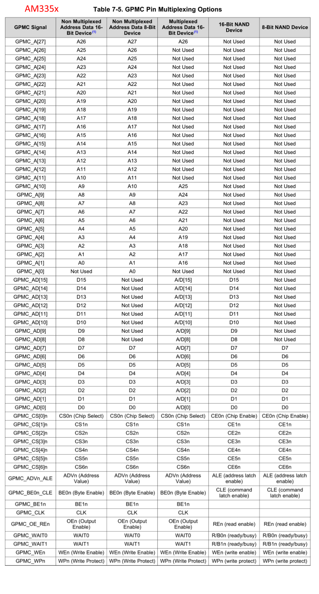
I am trying to connect NOR-FLASH with address / data-multiplexed and use it as a Boot Device as shown in P.604 Figure 7-3 of TRM.
Also in this figure, A [16: 1] / D [15: 0] is written on the AM335x side, and the address above it is A [27:17].
However, looking at Table 7-5., GPMC_A [1] is A16.
Probably a problem with the TRM notation, but if GPMC_AD [15: 0] is A [16: 1] / D [15: 0], then A [17] on the Processor side is A16 of GPMC_A [1]. Is that okay?
(Address on the Processor side is in 8-bit units, Address on the Memory side is in 16-bit units?)
Also, in the figure, A [27:17] is written as gpmc_a [11: 1], but in the table, A26 is GPMC_A [27]. Is this a typo in the figure?
In the table, GPMC_A [11] is "Not Used".

Best Regards,

Kouji Nishigata

  • Hi,

    I asked a question with a little confusion. Regarding the notation in Table 7-5, it was annotated that the LSB was written as A0. As a result, I understand that A17 from the AM335x side is output from GPMC_A [1] pin and connected to A16 of NOR-FLASH.

    However, regarding the pin output when A27 from AM335x, it seems that Table 7-5 and Figure 7-3 are different. Please tell me which is the correct answer.

    Best Regards,

    Kouji Nishigata

  • Hi Nishigata-san,

    I wanted to let you know that I am looking into your question. I should have an answer within 24 hours.

    Regards,
    Mark

  • Hi Nishigata-san,

    I see the issue in the TRM you described.
    I believe Figure 7-3 is correct and Table 7-5 GPMC Pin Multiplexing Options is wrong for the Multiplexed Address Data 16-Bit Device.
    I will refer to GPMC signals and the pins that they appear on.

    Other data manuals have the same GPMC Pin Multiplexing Options table but with the A[17] signal on A[2], and A[16:1] signals on A/D[15:0] pins for Multiplexed Address Data 16-Bit Device. Refer to the AM5728 TRM Table 15-445  GPMC Pin Multiplexing Options.

    Address Data multiplexed mode puts the least significant address bits onto the A/D bus. When using 16-bit data bus, the A0 signal is not used. A[0] is only used for a 8-bit data bus. So for a Multiplexed Address Data 16-Bit Device, the A[16:1] signals appear on the A/D[15:0] pins. The A[0] pin is not used, and A[17] appears on A[1] pin.

    In the AM572x TRM, the A[27] signal appears on the A[27] pin. I suspect AM335x is the same.

    I will confirm that AM3358 also operates this way, but due to the Thanksgiving holiday I will not have an answer until next week.

    Regards,
    Mark

  • Hi, Mark

    thank you for your answer.

    I think the addresses in the table in Table 7-5 point to the pin name of the Memory Device.
    On the other hand, the addresses in the table in Table 15-445 may point to the addresses output by AM335x.
    Since the Memory Device has a 16-bit wide address, if the LSB is written as A0, the A27 of the AM335x is connected to the A26 of the Memory Device, so neither table is wrong.

    What I'm curious about right now is that the high-level address connection in Figure 7-3 is written as:
    A [27:17]-> gpmc_a [11: 1]-> A [26:16]

    If A27 of AM335x is output from gpmc_a [27], I think it should be written as follows.
    A [27:17]-> gpmc_a [27,10: 1]-> A [26:16]

    Best Regards,

    Kouji Nishigata

  • Hi Nishigata-san,

    user1201164 said:
    If A27 of AM335x is output from gpmc_a [27], I think it should be written as follows.
    A [27:17]-> gpmc_a [27,10: 1]-> A [26:16]

    This is correct. The A27 signal comes from the A27 pin in 16-bit AD-mux mode. Refer to the below figure from the GPMC spec.

    Figure 7-3 is misleading - it incorrectly depicts the A27 signal on the A11 pin. The A11 pin is not used in 16-bit AD-mux mode.

    Regards,
    Mark

  • Hi, Mark

    thank you for your answer.
    My question has been resolved.

    If possible, please provide the original documentation for Figure 27.
    Also, do you request corrections to Figure 7-3?
    (Because we received a lot of inquiries about things that haven't been fixed recently)

    Best Regards,

    Kouji Nishigata