This thread has been locked.

If you have a related question, please click the "Ask a related question" button in the top right corner. The newly created question will be automatically linked to this question.

L138 PLL Clocking

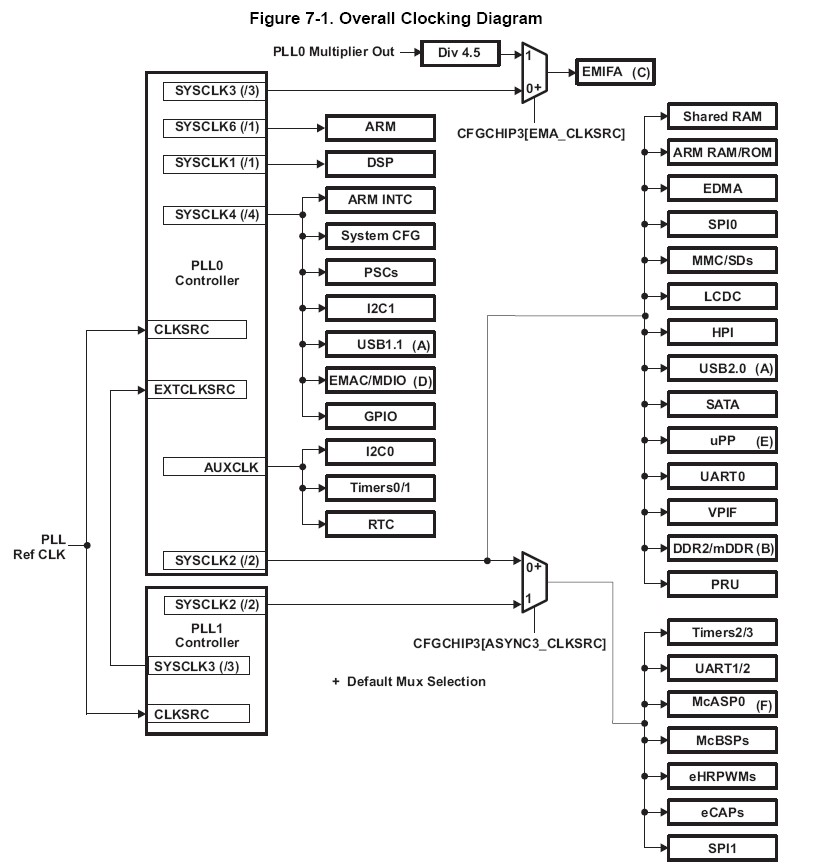
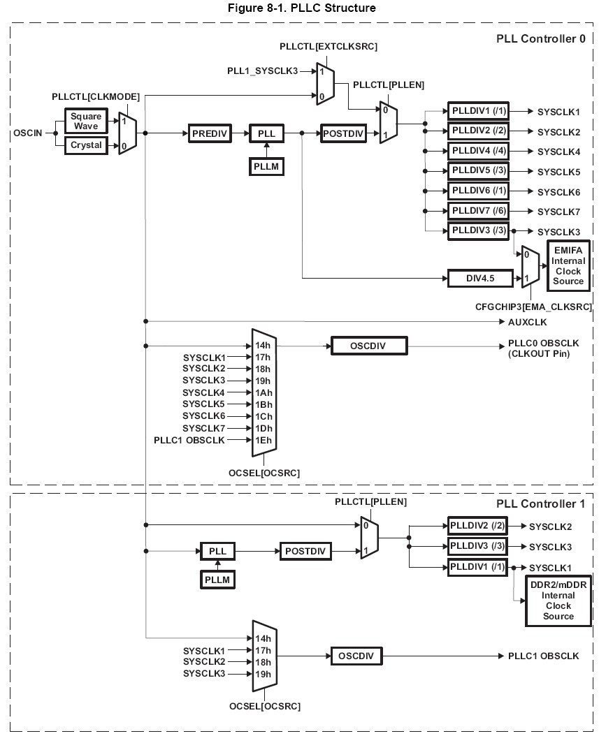
Hello

I am currently using both on board PLL controllers to drive all my peripherals.

In order to save battery life I am currently investigating the possibility of drive all my peripherals by only using PLL0.

However, there seems to be conflicting information within the Freon Reference Guide in regards to the clock tree.

Let's take for example the mDDR peripheral.

Under Figure 7-1 below, it can only be driven from PLL0, while from under FIgure 8-1, it can only be clocked under PLL1.


Is there a single diagram or spreadsheet that I can track for the whole system clock tree with dividers and clock gating registers so that I can ensure that if I do want to change my PLL clocks, I would like to easily indentify which peripherals will be affected.


  • tehoaislimau

    tehoaislimau said:
    Under Figure 7-1 below, it can only be driven from PLL0, while from under FIgure 8-1, it can only be clocked under PLL1.


    Have you reference the caption (B) in the clocking diagram? It points you to another section that explains the clocking for DDR2/mDDR


  • Hi,

    The 3rd clocking diagram is even more confusing.

    The below shows that the DDR module requires both PLL to be active, PLL0_SYSCLK2/2 to drive VCLK and PLL1_SYSCLK1 to drive the DDR PHY.

    This diagram does not match what was shown in the above clock tree.


    I just need to know which to follow and if there is a possibility of running everything with just one PLL0?

  • tehoaislimau -

    tehoaislimau said:
    This diagram does not match what was shown in the above clock tree.

       I looked at the clocking diagrams, and they appear to match to me. Figure 7-3 shows that VCLK is supplied through PLL0_SYSCLK2/2 (Poor working perhaps, but this a a divide-by-two of PLL0_SYSCLK post CHIPCFG3[ASYNC3_CLKSRC] Mux). It also shows that DDR PHY clock is supplied from PLL1_SYSCLK1. This same connection is shown in Figure 8-1 post PLLCTL[PLLEN] Mux as well as post PLLDIV1 clock divider.


    However, note that PLL1_SYSCLK1 can be derived from the output of the internal oscillator (see figure 8-1) by configure the Mux PLLCTL[PLLEN] to select input 0.


    tehoaislimau said:
    I just need to know which to follow and if there is a possibility of running everything with just one PLL0?

    If depends on all the peripherals you wish you use. If you can supply a list of the peripherals you want to use in your system, we can help you figure out the clocking options for each one based off the clocking diagram.


  • Hi

    Thanks for your replies.

    From the mDDR block diagram, it seems that regardless of what peripherals I am using, the mDDR already dictates that both PLL would be required.

    Can you confirm this is intended?

    PLL0 would be used for VCLK and PLL1 would be used for DDR PHY... seems that there is no way out