This thread has been locked.

If you have a related question, please click the "Ask a related question" button in the top right corner. The newly created question will be automatically linked to this question.

AM6548: SerDes Reference Clock Distribution

Part Number: AM6548

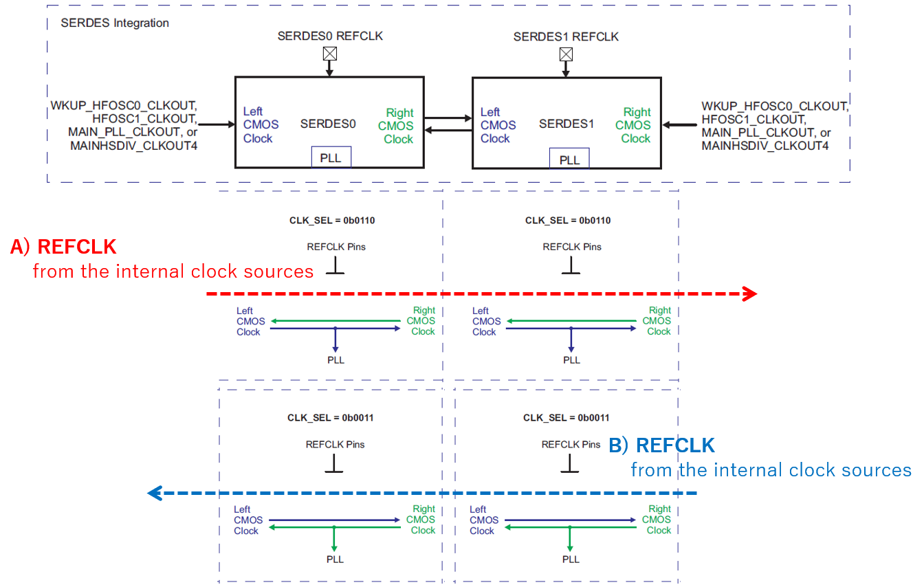
In Figure 12-1856 on TRM, the colored lines in the diagrams indicates the possible REFCLK distribution for the adjacent SerDes.

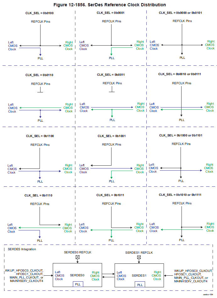
The colored (green) lines only come from the Right CMOS Clock in the diagrams.

Do the colored (green) lines indicate that the REFCLK coming from the adjacent SerDes can come only from the Right CMOS Clock?

Can the REFCLK coming from the adjacent SerDes come from the Left CMOS Clock?

Can the REFCLK coming from the internal clock sources come from both the Right CMOS Clock and Left CMOS Clock?

If same REFCLK is distributed to both SERDES0 and SERDES1, is it required that the REFCLK comes from the SERDES1 side?

Best regards,

Daisuke

  • Hi,

    I have some additional questions.

    Please tell me how REFCLK is distributed to the REFCLK outputs (REFCLK0N/P, REFCLK1N/P).

    Can the REFCLK come directly from the internal clock sources to the REFCLK output without pass through SerDes?

    Can the REFCLK come from the the SerDes side (REFCLK Pins or adjacent SerDes) to the REFCLK output?

    If same REFCLK is distributed to both SERDES0 and SERDES1, can both the REFCLK outputs (REFCLK0N/P and REFCLK1N/P) be used for two external devices?

    If same REFCLK coming from the internal clock sources is distributed to both SERDES0 and SERDES1, should the REFCLK comeing directly from the internal clock source to the REFCLK output without pass through SerDes be used for a single external device?

    Best regards,

    Daisuke

  • Hi,

    Could you answer the questions in my posts above?

    I would like to know how to distribute REFCLK when using PCIe as a single 2-lane port and Root complex.

    Please give me an answer as soon as possible. Your prompt reply would be appreciated.

    Best regards,

    Daisuke

  • Daisuke Maeda said:

    I would like to know how to distribute REFCLK when using PCIe as a single 2-lane port and Root complex.

    If same REFCLK coming from the internal clock sources is distributed to both SERDES0 and SERDES1, which of A) and B) in the figure below should be used?

    In that case, which of REFCLK0N/P and REFCLK1N/P should be used as the REFCLK output to a single external device?

    Please give me an answer as soon as possible. Your prompt reply would be appreciated.

    Best regards,

    Daisuke

  • Dear TI support team,

    Could you answer the questions in my posts?

    Could you point me out if I have any misunderstandings?

    Please give me an answer as soon as possible. Your prompt reply would be appreciated.

    Best regards,

    Daisuke

  • Daisuke, 

    I understand you like to configure the PCIe as 1px2L RC, and then drive out a REFCLK to the EP via the slot. In this case, please note the following:

    1. In 2-lane mode, the two SERDES MUST chain their refclk. i.e., you can either use SERDES0 or SERDES1 to obtain refclk (either from REFCLK input pins, or from internal PLLs), then the other SERDES MUST obtain its refclk from its neighbor via chaining. We have verified either chaining leftward or rightward would work. 

    2. To refclk output signal is directly driving out of SOC DIRECTLY from the mux output that feeds the SERDES. i.e., say you choose MAIN_PLL_OUT to drive a 100MHz refclk to feed SERDES0, this 100MHz clock is simultaneously sent out to the REFCLK out pins, upon converting to differential signals. this way you can implement common clock PCIe architecture.  Note again in this case, the SERDES1 gets its refck from SERDES0. 

    If you are using Linux SDK, the standard Linux SD card images will recognize the IDK (vs. GPEVM), and therefore the correct device tree files are loaded that enables 2Lane RC port with REFCLK enabled on the slot. 

    If you are using RTOS SDK, you may use "BOARD=am65xx_idk", that will enable macros in source code to use PCIe controller 0 and get SERDES configurations right. The REFCLK output is not enabled by default in RTOS, you may use following reference to find the mux control of the refclk output. 

    /* CTRLMMR_SERDES0_REFCLK_SEL Register 0x0010_8020[1:0] = 0x2, MAIN_PLL_CLKOUT
    CTRLMMR_SERDES1_REFCLK_SEL Register 0x0010_8024[1:0] = 0x2, MAIN_PLL_CLKOUT
    */
    CSL_FINSR(*(volatile uint32_t *)(CSL_CTRL_MMR0_CFG0_BASE + CSL_MAIN_CTRL_MMR_CFG0_SERDES0_REFCLK_SEL), 1, 0, 0x2);
    CSL_FINSR(*(volatile uint32_t *)(CSL_CTRL_MMR0_CFG0_BASE + CSL_MAIN_CTRL_MMR_CFG0_SERDES1_REFCLK_SEL), 1, 0, 0x2);

    I think most of your questions should be answered once we clarify that REFCLK is directly driven out of the SOC vs. from SERDES. Please pls reply back if you still have questions. 

    JIan

  • forgot to mention - IDK is the same baseboard with the 2Lane PCIe daughter card. vs. GPEVM will a 1xlane PCIe slot. 

    regards

    Jian

  • Hi Jian-san,

    Thank you for your reply.

    I was confused by the following description in section 12.2.4.3.1.2 on TRM.

    "The colored lines in the diagrams indicates the possible REFCLK distribution for the adjacent SerDes. For
     the side without an adjacent Serdes, clock output is tie off."

    I understand that the color lines are indicate both black and green lines, and the REFCLK does not distribute if there is no PLL or no adjacent SerDes at the end of the arrow.

    Best regards,

    Daisuke