This thread has been locked.
If you have a related question, please click the "Ask a related question" button in the top right corner. The newly created question will be automatically linked to this question.
Part Number: J7
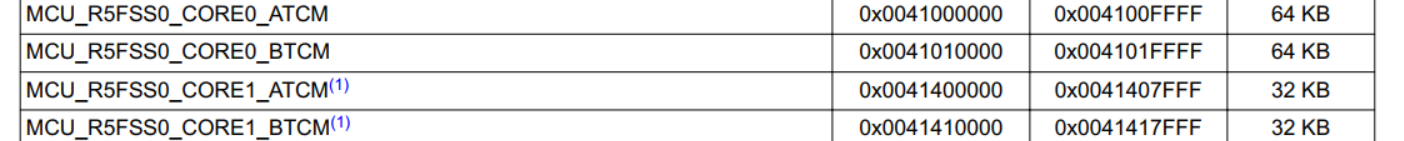
I would like to ask a question in DRA821, the ATCM of CORE0 has 64KB, CORE1 has 32KB.
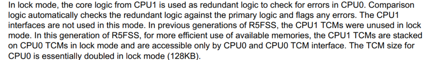
The MCU memory map only has 32KB, but according to the description later in the lock step mode TCM has 128KB available, which means this ATCM should be 64KB,
Then how to address this, the first 32KB with local address and the next 32k with global address?
Hello,
When I look in the TRM and underlying functional specifications what I see described is each R5 CPU has 64KB of TCM memory.
There is 32KB in TCMA and 32KB in TCMB. So when running as 2-R5's, R5F0 has 32K and R5F1 has 32K of "actual backing sram memory".
When in lock step mode the TCM memory stacks. As such only the R5F0 is visible from a programmers point of view. In this lockstep case R5F0 has 128K of TCM memory visible. 64K in TCMA and 64K in TCMB.
I interpret the above memory address map is constant with that description. It has defined 128K of address space for R5F0 to cover the lock step case. When not running in lockstep the size of actual memory backing that address space would only be 32K.
Address space in a memory map does not necessary mean there is physical memory backing it. A common example is DDR. There may be giga-bytes of reserved address space for DDR in a system but a design doesn't need to populate it.
Regards,
Richard W.