

Hi All,
I would like to ask a question on component footprints.
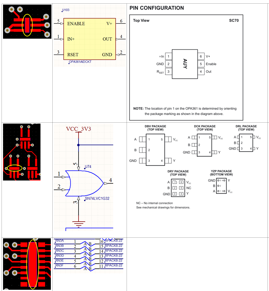
I have found several components have additional, unnecessary copper region with them in EVM6437 PCB file, and some of them are shown here.
What are the red regions (circled in yellow) locating within the component footprints? I checked each of the components’ data manual and found none of them requires additional copper thermal land (as those for PowerPAD), so I don’t see any reason why these additional copper regions are added.
These components with copper region between their pins are:
|
1 |
OPA361 amplifier |
|
2 |
SN74LV1G32 logic gate |
|
3 |
Resistor pack |
[3 Resistor pack] is especially common and I haven’t noticed the existence of pins/conducting parts right below it, and for it why the copper region under footprint is added?
Thanks,
Zheng

