Other Parts Discussed in Thread: OMAP-L138, OMAPL138
On my OMAP-L138-based custom board, I am trying to implement the Gpio_example in the PSP 1_30_01 CSLR examples. However, I am not able to set the PINMUX properly since, apparently I cannot access the Kick registers. Below is a code snippet from the first part of main.c
void main (void)
{
/* This function will configure an GPIO pin as an interrupt pin */
/* Key to be written to enable the pin mux registers for write */
sysRegs->KICK0R = 0x83e70b13;
sysRegs->KICK1R = 0x95A4F1E0;
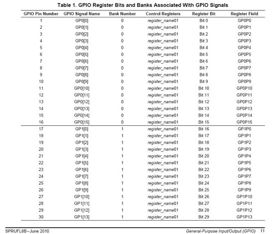
/* enable the pinmux for the GPIO bank 0 pin 7 */
// sysRegs->PINMUX1 = ((CSL_SYSCFG_PINMUX1_PINMUX1_3_0_GPIO0_7)
// << (CSL_SYSCFG_PINMUX1_PINMUX1_3_0_SHIFT));
sysRegs->PINMUX1 = ((CSL_SYSCFG_PINMUX5_PINMUX5_7_4_GPIO2_14)
<< (CSL_SYSCFG_PINMUX5_PINMUX5_7_4_SHIFT));
When I step through the code and watch the KICK0R and KICK1R registers, they are set to 0x00000000. What can be causing this?
Thx,
MikeH