This thread has been locked.

If you have a related question, please click the "Ask a related question" button in the top right corner. The newly created question will be automatically linked to this question.

TMS320C6713B boot problem

Other Parts Discussed in Thread: TMS320C6713B

Hi all,

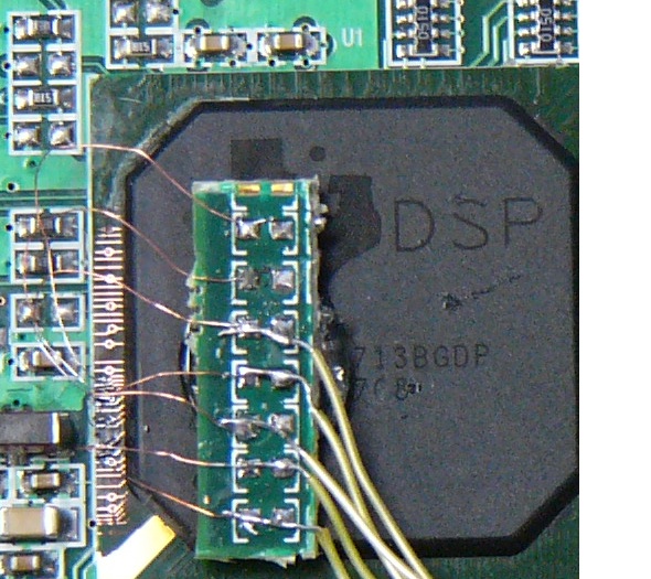
In our design we are using the TMS320C6713B DSP and MT48LC32M16 SDRAM. During boot we can face the following problem: The DSP will hang up itself every now and then. It is very unpredictible but it is quite easy to reproduce, all we have to do is to reboot our board many times untill it crashes. When this happens, the DSP will hang itself up and will not generate an EMIF-clk anymore. This way, our entire system crashes, since we depend on this clk.

We tried several things and we found that when we tie the CKE-pin of the SDRAM to gnd, the DSP will boot up, and will generate the EMIF-clk. Of course, this doesn't solve our problem, since the SDRAM will not function anymore, but the DSP doesn't hang itself anymore. According to the datasheet, the CKE-pin can be tied to VCC without problems, but it does give us a problem. Is this a known issue and is there a workaround for this issue?

Regards,

Danny Jacobs

  • Sorry, this doesn't sound like any issues I'm familiar with.

    Questions

    • Are you booting from NOR flash?
    • I assume you have written a secondary bootloader that resides in the first 1k of flash that loads your primary app, right?

    Suggestions:

    • In general, simplify the program into you get to something that consistently works.  For starters perhaps you could simply put a spin loop (perhaps that toggles a GPIO for observability) in the first 1k of your flash.  In other words, chop out your main application, peripheral configuration, etc to have something really simple.  Then start building back up...
    • Add your PLL configuration code back in.
    • Add your SDRAM configuration code back in.
    • Add your application loader back in (but don't branch to the application).
    • Put a spin loop early in your application so it doesn't fully execute.
    • If everything is still good at this point you may need to pare down your application too...

    All of the above is mostly geared toward a software issue.  Of course this could also be a hardware issue.  I recommend that you or a colleague review your design.  You might want to look at the Hardware Design Checklist for some tips on things to check.

  • Hi Brad,

    We are indeed booting from NOR flash. Why do you ask?

    In our flash, we have two images: 1 for an FPGA and 1 for the DSP. We first boot the FPGA from flash and when the FPGA is booted, we remove the reset to the DSP and the DSP will start booting from flash via the FPGA. The DSP doesn't know that the FPGA is between the flash and the DSP, since it's a transparent "buffer" so to say.

    Regards,

    Danny

  • Danny Jacobs said:
    We are indeed booting from NOR flash. Why do you ask?

    In order to help you debug your boot problem I need to know which boot mode you're using.

    Danny Jacobs said:
    In our flash, we have two images: 1 for an FPGA and 1 for the DSP. We first boot the FPGA from flash and when the FPGA is booted, we remove the reset to the DSP and the DSP will start booting from flash via the FPGA. The DSP doesn't know that the FPGA is between the flash and the DSP, since it's a transparent "buffer" so to say.

    So does the DSP image consist of a 1KB secondary bootloader which configures PLL, SDRAM, and then loads the rest of the code?

  • Brad Griffis said:
    So does the DSP image consist of a 1KB secondary bootloader which configures PLL, SDRAM, and then loads the rest of the code?

    Yes, this is our configuration.

    Currently we are still investigating this issue, but we possibly have found the problem. Our PCB also contains a JTAG-chain, with an FPGA, some other devices and the DSP. When we break the chain (so the boundary scan-pins of the DSP are floating), we no longer experience this issue. Is it possible that during a boot-cycle, if perhaps some garbage-data appears on the boundary-scan pins, the DSP is forced into JTAG- or emulation mode?

    Regards,

    Danny

  • Make sure you have 4.7k pullups on EMU0 and EMU1 as well as a 4.7k pulldown on nTRST.  That should ensure the device powers up cleanly, assuming nothing else is driving those signals.

  • Brad Griffis said:

    Make sure you have 4.7k pullups on EMU0 and EMU1 as well as a 4.7k pulldown on nTRST.  That should ensure the device powers up cleanly, assuming nothing else is driving those signals.

    We would like to use the dsp in boundary scan mode in order to test the pcb's before they will be released. So we have EMU0 and EMU1 driven to ground with a 1k0 pull-down. nTRST is pulled down with a 4k75 pull dow, however we have 2 devices connected to this wire which have an internal pull up.


    Regards,

    Danny

  • EMU0 and EMU1 need to be pulled high.  Your test fixture should drive them low to do boundary scan.

  • Brad Griffis said:

    EMU0 and EMU1 need to be pulled high.  Your test fixture should drive them low to do boundary scan.

    OK, understood... But what's the difference when those lines are pulled down? When we have garbage on our boundary-scan lines (perhaps to a design-flaw that we made), the DSP will start up in Boundary Scan-mode, also making it boot incorrectly, right?

    Regards,

    Danny

  • The EMU0 and EMU1 pins get latched on the rising edge of TRST.  You said there are some opposing (weak) internal pullups on the TRST line.  My guess would be that some of the junk from the other JTAG pins gets coupled onto TRST which might be enough for it to SOMETIMES latch EMU0/1.  The device will definitely fail to boot if you have EMU0 and EMU1 low and the device sees a rising edge on TRST.  If the noise was a little greater on TRST then you would probably never boot, but since you probably have some small amount of noise it probably only happens sometimes.  A stronger pull-down on TRST might also do the trick.

  • We dit see some garbage on the trst-pin, that's correct... But doesn't the DSP go into emulation mode when EMU0 and EMU1 are tied high and there is some garbage on the trst-pin?

  • Danny Jacobs said:
    But doesn't the DSP go into emulation mode when EMU0 and EMU1 are tied high and there is some garbage on the trst-pin?

    Yes, it does.  That could potentially cause an issue.  However, having it go into boundary scan will cause a MUCH bigger issue. 

    I don't think there's anything more to say.  You need to have pullups on EMU0 and EMU1, and a pulldown on TRST. 

  • Ok, this didn't help... The DSP still hangs itself occasionally... Is there a certain sequence in which the voltages of the DSP should appear? The DSP doesn't respond on anything and a power cycle is the only way to reset the DSP again. It doesn't start trying to read it's bootloader or anything...
  • There's no power sequencing requirement for this device. For your testing are you power cycling each time, or are you pulsing the reset pin to test this out? Search the data sheet for "do not oppose" and make sure those pins are all at the proper state (high for pins with internal pullup and low for pins with internal pulldown) when reset is released.
  • Hello Danny,

    I see that there is a resolved checkbox on this thread, yet the last posts seem to indicate that the issue was still unresolved.  Did you find something that fixed your issue?  We seem to be having a very similar issue, and I very interested to hear if you did indeed find a solution that was other than the JTAG pins.

    Thank you!

    Katherine

  • Hi Katherine,

    We had the problem that our FPGA asserted the HOLD- or the HOLDA-pin during booting of the DSP. I don't remember exactly which one it was, but this was a bug in our FPGA... Our FPGA boots first and then the DSP. Perhaps you experience the same kind of problem?

    Regards,

    Danny

  • Hi Danny,

    Thanks for the post.  I just rechecked our schematic, and both our HOLD and HOLDA pins are N/C.  So... your fix isn't going to be our fix, unfortunately.  It is good to know you did indeed solve the issue, and thanks again for replying!

    -Katherine

  • Greetings,

    You may consider putting a PU or PD on the un-used pins, unless it is explicitly said in the device DS they have no effect.

    Good Luck,

    Sam

  • Sam makes a good suggestion.  Which package are you using?  Can you physically access the HOLD pin/ball (perhaps using a via)?  (HOLDA is the "acknowledge" pin, so that one isn't critical.)  If so, it would be a good test to wire that pin to DVDD.

  • Hello,

    Unfortunately we cannot access those pins - we have a BGA package and those are not fanned out so there is no via to tap.

    -Katherine

  • Greetings,

    Even with the BGA package, one can get lucky in finding the trace/via for the HOLD on the FR4 package carrier (to side of the BGA), and apply such an experiment.  I had to do that in my previous life on the C6713, see attached pic.

    Good Luck,

    Sam

  • Very interesting... I'm OK with defacing the FR4 carrier for this test.... but I cannot tell from the picture which pin is which trace on the FR4 carrier.  Is there some governing document or could TI kindly point out the location of the HOLD trace on the -ZDP package, -300 part?

    Thanks,

    Katherine

  • I'm sorry, but I won't be able to find/distribute that sort of info.  I think you're better off going with the minimal software build mentioned in your other thread for the time being.

  • Greetings,

    From the C6713 Datasheet and the pic below

    You can use a bare part, shave off the green epoxy, ohm out the J17 ball to the facial trace/via and then realize your PU/PD on a part on one of your platforms.

    Good Luck,

    Sam

  • Greetings,

    You may not need to do this exercise, since the HOLD pin has an IPU enabled, according to the device DS.

    Good Luck,

    Sam