This thread has been locked.

If you have a related question, please click the "Ask a related question" button in the top right corner. The newly created question will be automatically linked to this question.

DRA718: adjustment of pad diameter or single-ended impedance

Part Number: DRA718

Hi,

My customer is doing artwork with DRA718 and having difficulties in pattern routing due to the tightness of the space between pads.

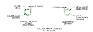
The recommended pad size is 0.35, but can we reduce it to 0.3mm to have more space between pads?

If PAD size cannot be reduced to 0.3mm, my customer would like to increase single-ended impedance (greater than the minimum value of 50ohm) to reduce the pattern width - and the DDR3 termination impedance will be adjusted accordingly.

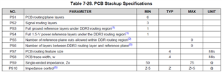
Is it common to use the single-ended impedance higher than 50ohm?

Please let me know how to secure more space between pads and make routing between pads easier - 1) reduce pad size to 30mm, or 2) use higher single-ended impedance than 50ohm.

Thanks.

Regards,

James

  • It is recommended to stay with the 0.35mm pad size, as the creates the strongest solder bond between PCB and device.  Customer will often slightly reduce the trace width in BGA areas due to pad/spacing requirements, and then widen the trace to meet specific impedances once the BGA area is escaped.  It may be OK to use higher impedances (> 50-ohms).  Typically for DDR interfaces, the lower impedances are better due to higher drive strengths.