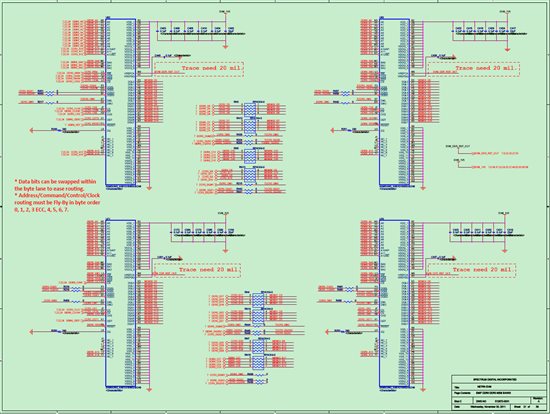
Hello,everyone,when I designed my project I found the design of Dm8168 SDI's Demo schematic "evm8168x_Orcad_RevG DSN" The SH21-EVIF DDR0 BANK0 page DDR controller data lines D0-D7,D8-D15,D16-D23,D24-D31 and four chips 8-bit DDR chips are not exactly correspond to D0-D8,please question how is this going?Thank you! See picture.
My email is:xrf83@126.com


