This thread has been locked.

If you have a related question, please click the "Ask a related question" button in the top right corner. The newly created question will be automatically linked to this question.

Proposed Method for using TPS65217C with AM335x RTC only mode

Other Parts Discussed in Thread: TPS65218, TPS65217

I received some comments via email from a TI engineer names Siva cautioning us regarding our plan of using LDO1 to power VDDS and LDO3 for VRTC.  We are using the TPS65217C, and want to use RTC only mode.  Transferring this conversation to e2e in hopes of closure over the weekend.

From TI:

There are some considerations that need to be followed while doing the rail assignments for VDDS using TPS65217C:

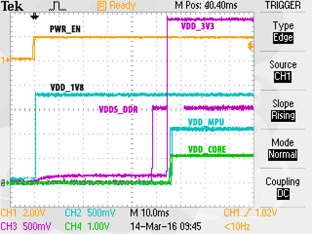
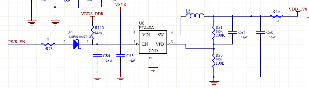
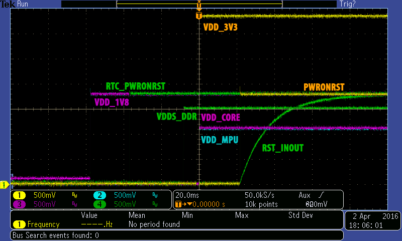
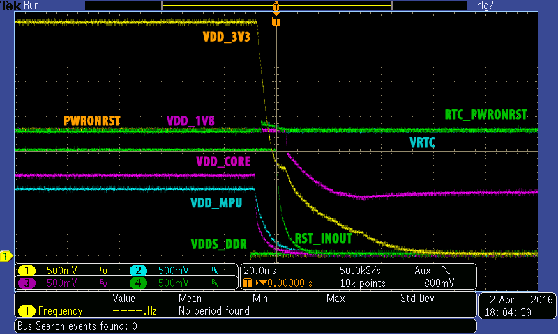
  1. AM335x requires the VDDS supply to be the [First?] powered ON. Given the power sequencing on TPS65217C, LDO1 is the one that is powered first. So, VDDS has to be assigned to LDO1
  • Additionally, if there are any other IO’s configured as 1.8V i.e. any of VDDSHVx[1-6] configured as 1.8V, it is preferred to have them powered by LDO1 since VDDS and VDDSHVx[1-6] configured as 1.8V should be powered from same source i.e. LDO1. Note that load current on LDO1 is limited
  1. LDO1 was initially dedicated for RTC supply and given that TPS65217C requires LDO1 for supplying other rails, RTC only mode cannot be supported with TPS65217C and will cause a data sheet power sequencing violation
  2. Earlier versions of TPS65217C user guide had incorrectly assigned LS1/LDO3 to power AM335x VDDS rail. This assignment violates our AM335x data sheet power up sequencing. We worked with the PMIC team to get this addressed and therefore has changes in the Rev-I user guide. TPS65217C is programmed to have rails come up as LDO1 -> DCDC1 -> LS1/LDO3 -> LDO2 -> LDO4 -> DCDC2/3.
  3. Given the customer situation, the best action is to use TPS65218 instead of using TPS65217C. This will resolve concerns in using RTC only mode along with having proper rail assignments for VDDS and VDDSHVx[1-6]configured as 1.8V. Let me know if you’ve any further questions.

  • My Follow up:
    I don’t see any reference in the datasheet figure 6-4 at all about VDDS in the power sequence. Can you clarify what you mean by VDDS so I can interpret your comment more accurately?

    As my circuit is configured, I have VDD_RTC on LDO1, VDDS_DDR on DCDC1, VDD_1V8 on LDO3, Nothing on LDO2, VDD_3V3 on LDO4, VDD_MPU on DCDC2, and VDD_CORE on DCDC3. The order that I listed them is the startup sequence as well. According to figure 6-4 in the am335x datasheet, I should be starting in the sequence RTC -> 1V8 followed by DDR -> 3V3 -> MPU& CORE. So I have 1V8 and DDR swapped in the sequence. Is that correct?

    We are using both the backlight and the battery charger on the TPS65217c, so the …218 causes us to lose quite a bit of function. If we must, I would rather eliminate the RTC only operation, and use a separate RTC device, or add an additional power supply, as proposed below.

    A note on our expected mode of operation, perhaps this changes your recommendation. We do not expect to actually power down the system, but always leave RTC power on. The only exception to this is initial power up, reset, and if the battery dies. Also we will be using standby mode. We have a prototype board built in the way of the schematic you have seen, and it is working fine as far as we can tell.

    I propose that a reasonable solution is to connect a separate regulator for the 1V8 component, and activate it with the PWR_EN signal. To manage shutdown sequence, I would propose that the 1V8 regulator be controlled with PWR_EN or’d with VDD_DDR. This would turn it on when PWR_EN is applied, and then turn it off only after the DDR voltage has dropped (making it the last thing to turn off). Will this work to achieve the required sequence?
  • Hi,

    This is currently under investigation. Feedback will be posted here.
  • Another option I'd like your feedback on is gating the VDDS_DDR with a load switch, driven by the 1.8V rail. This would result in the VDDS_DDR not coming up until [slightly] after the 1.8V rail. I think if the load switch were on the input side of the DCDC1, the the PGOOD_SIGNAL would also continue to work, which would be a nice-to-have; but it is possible that this could create problems for the regulator.
    The benefit of this approach is much parts, keeping the PGOOD signal, and simpler logic controlling the switch, since an or-condition as described with the regulator solution would not be required. I am only drawing 250mA on the 1.8V rail, so I don't need the extra power that I have available with the external regulator.
  • I ran a test of the proposed solution, driving PWR_EN to a separate regulator.   It seems to have resolved the sequence issue.   Please note that this is  photoshop overlay of two runs of the scope - so there are a couple of weird artifacts.  Please advise.

  • VDDS supply is used for the dual-voltage IO's. Snapshot below from Data sheet listing the corresponding BGA's for ZCE and ZCZ package. This is a 1.8V nominal voltage supply. I think you have this supply grouped with other 1.8V supplies and referred to as VDD_1V8.

    Given the clarifications on your use mode and the fact that you are using the LED drivers, I think your approach of powering VDD_1V8 or VDDS_DDR with an external regulator and managing the sequencing should work.

    In the proposal that you implemented for which you shared the scope plots, can you describe how you connected the PMIC_POWER_EN from AM335x to the PMIC and to the external 1.8V regulator? Can you overlay the VDDS_RTC on this plot?

    Lastly, but most importantly, how does the power down look with this scheme?

    Regards, Siva

  • Siva - I believe that you will receive my schematic under NDA via email.

    for the record., the PMIC_PWER_EN line is connected directly between the enable input of the external switching regulator and the PMIC.   So this is why you see the 1.8 V coming on so quickly.

    Below is a scope shot showing part of the power down sequence.  In the simple case of connecting POWER_EN directly to the enable, the 1.8 volts ends up being the first thing to power down.  I will work on a complete power sequence for you, instead of only the 1.8V and DDR voltage that I have available in the image below.  Red trace is 1.8V and Blue is VDDS_DDR.

  • I think I know why you wanted to see VRTC - my mistake was thinking that it would always be on.  Actually it comes on with with the button press.  So is there enough time between VRTC coming up and VDD_1V8?  The datasheet says that it can be ramped independently.

    Poweroff you can see that the RTC voltage stays up, but that the 1V8 drops immediately, before everything else (and it is supposed to be last in the sequence)

  • I've tested the following solution, and it looks good to me; I'd love to hear some comments while I still have time to change it.

    When I test this, I see the following:

    BLUE = RTC
    YELLOW = 1V8
    MAGENTA = 3V3
    GREEN = DDR
    Power up.  [Note that the leakage onto 3.3V has been resolved, I just don't have a full power sequence scope shot]
    the VDD_MPU and VDD_CORE voltage are last, after the 3.3V, but are not shown.
    Power down from command line:
    In my book, this works.  Can I get a thumbs up from TI?
  • I’m still struggling to see the full picture of the power-up/down sequencing along with the PWRONRSTn/RTC_PWRONRRSTn. However, the specific power down snapshot that was sent looks fine. There are a couple of other options that you can also consider here.

    Also, there seems to be some leakage into the 3.3V that needs to be fixed. The RTC rail also has a small glitch when switching from main power to battery. Please make sure the RTC power is measured after you changed the pull-up resistor to the VRTC rail

    Option 1:
    Use TPS65217B + DC-DC for external DDR3 Memory + Processor and use LDO2 as the EN strobe. This will make sure that the sequence is as per data sheet and uses the TPS65217 sequencer

    Option 2:
    More intrusive change, but you could potentially use LPDDR1 or DDR2 with AM335x if the memory type work and you can completely avoid an extra rail. LPDDR1 will especially help if you are looking for optimizing power overall
  • Siva - beena bit of a delay, because I wanted to capture the waveforms on the final board.   I think these look good. I hope you agree.   In either case, please provide your feedback:

    Power on:

    Power Off: