This thread has been locked.

If you have a related question, please click the "Ask a related question" button in the top right corner. The newly created question will be automatically linked to this question.

OMAPL138B-EP: questions on DRAM timing diagram & interfacing to OMAPL138

Part Number: OMAPL138B-EP
Other Parts Discussed in Thread: OMAPL138, OMAP-L138

Hi,

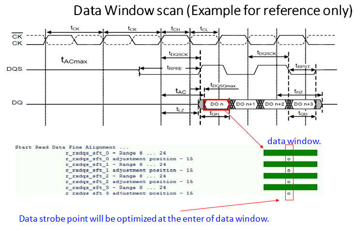
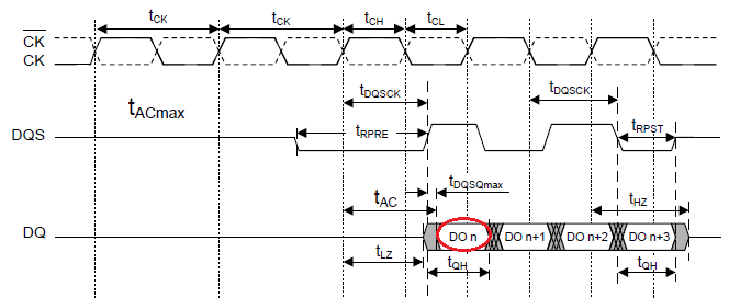
With reference to WinBond DRAM diagram below, 


So if we were to interface this with OMAPL138,

1) Will the data "read" state based on DQS or CLK?

2) What will the "valid data window" to implement for the stage highlighted red above?

Regards,

Leo

  • Hi Leo,

    I am checking with the designer to confirm whether the CLK edge or the DQS edge is used.

    I should hear back today or tomorrow.

    Regards,
    Mark

  • Hi Leo,

    For all DDR interfaces the PHY sits between the controller and the IO’s talking to the DDR memory. The PHY uses clock to launch all signals to the DDR.
    The DDR devices uses the clock to latch all command/address signals, and DQS to latch write DQ/DM. Similarly, the PHY uses DQS to latch read DQ.

    For writes to the DDR memory, the valid data window is centered around the DQS edge.
    For reads from the DDR memory, the valid data window is edge aligned with the DQS edge. The PHY has a DLL that is locked onto the DQS and performs a 90 degree phase shift on the DQS signal before using this recovered edge to latch the data.

    Refer to the JESD79-2 DDR2 JEDEC Specification or one of many available appnotes online (search for something like "ddr memory dll dqs edge aligned centered"). The JEDEC specification provides tables and calculations for setup and hold time.

    What problem are you specifically trying to solve? If its performing timing analysis for a DDR2 memory, we provide routing guidelines for robust DDR2 performance instead of providing signal timings. Refer to the DDR section of the datasheet. The DDR2 controller on the OMAP-L138 is compliant to the JEDEC specification, which conveys the timing and signal integrity requirements.

    Regards,
    Mark
  • Hi Mark,

    For read from the DDR Memory, except performing DQS at 90 degree phase shift,  do OMAP-L138 system also provide the fine tune step?

    This is refer to the flexibly to optimize the strobe point as illustrated by diagram below. 

  • Hi Mark,
    Kindly advise on the query posted by Kean Hua above as it's been pending for more than a week, Appreciate it much. Thanks!

    Regards,
    Leo
  • Hi Leo,

    I have replied to this question on another thread: e2e.ti.com/.../749156

    Fine tuning of the 90 degree phase shift performed by the PHY is not a supported feature. Routing guidelines must be followed within tolerance.

    Regards,
    Mark