This thread has been locked.

If you have a related question, please click the "Ask a related question" button in the top right corner. The newly created question will be automatically linked to this question.

AM5K2E02: Booting from NAND Flash Issues

Part Number: AM5K2E02

Hi,

For context, We are testing a custom PCB with a AM5K2E02 SOC. We can connect to the board using CCSv8 and XDS100v2 and are able to load and run basic programs. One of these basic programs reads/writes from the attached NAND flash using the EMIF interface. The reads/writes are successful.

When configuring the boot pins to boot from UART we are able to boot and run a program. However when loading a GP header image into NAND flash the processor does not boot.

The flash part is S34MS01G200TFV000 and should be compatible. The program we are using to write and read flash, is using code taken from the TI nandwriter located \ti\pdk_k2e_4_0_12\packages\ti\boot\writer\nand\ which has been modified to build for the AM5K2E02 instead of the C66x DSP. This should ensure the ECC and data is written to flash correctly.

I'd like to verify the following:

- The flash part is compatible with the bootloader and the bootloader is reading the flash geometry correctly and attempting to boot.

- The programmed image I have written to flash is of the right format (GP Header). Could an example file be provided? I have written it to every block in flash to avoid the RBL skipping bad blocks to be an issue.

I have will attach.dat files of the boot ROM Log and Trace data located at 0x0c1b0300  and 0x0c1b1fe0 captured shortly after power on (see reply below), similar to what was requested on this thread e2e.ti.com/.../2819493. If source cannot be provided so I can debug, can someone assist in telling me what the bootloader is doing?

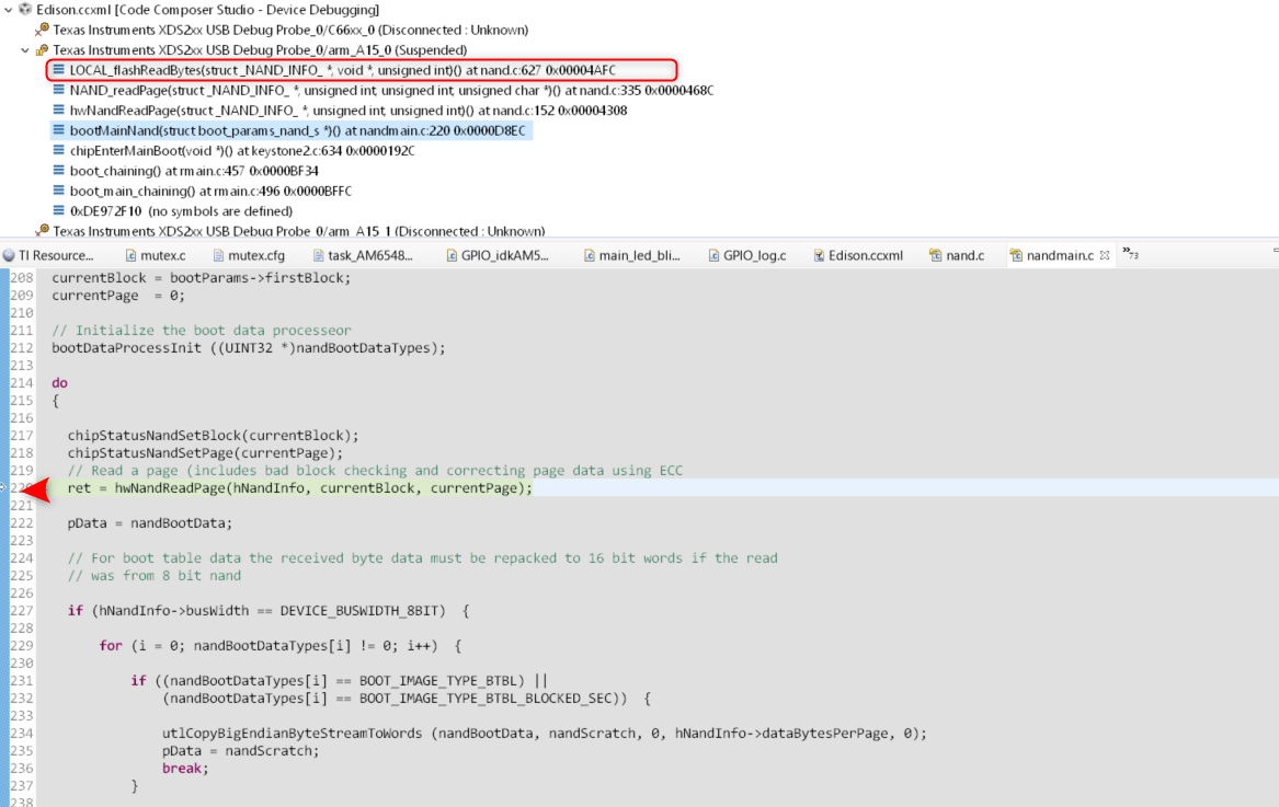
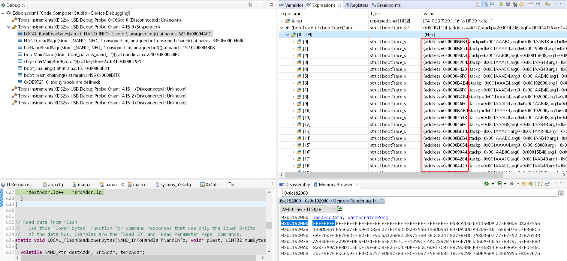
Using the debugger I can see the PC seems to be around 0x4AFC most the time, sometimes it is just stuck at 0x9B8 which I understand to be an error state.

(0x02620020) DEVSTAT Value: 0067

(0x0C1B0500) Boot Parameter Table: 

002A 0000 0050 0000 4019 0102 0000 0000 04E2 04E2 0001 0001 0000 0000 0000
0000 0000 0000 0000 0002 0000 0000 0000 0000 0000 0000 0000 0000 0000 0000

As you can see, many vital fields in the Boot Parameter table for the NAND boot mode are 0's. Does this indicate an issue? When using UART the fields are all filled in correctly, here there is only the chip select and block to boot from (0 anyway).

I am happy to run more tests and provide more data to understand why the boot is not completing.

Thanks,

Jasvinder

  • Reply with Trace and Boot log .dat files Trace.datBootLog.dat

  • Jasvinder,

    Thanks for providing the details. The fact that you are able to boot over UART indicates power sequencing on the board is good but have you confirmed if the NAND flash is powered up before the SOC can read from it?

    I also see that the DEVSTAT is similar to what we set on the TI EVM (0x00010067) so I don`t see any issues with that.  The interesting thing that I was able to observe with the EVM is if I configure NAND boot with no image on the NAND , the PC of the A15 hangs at the same place as 0x4AFC so i loaded the ROM symbol table to find the function being executed and found that this is one of the first functions in the ROM where is is trying to read the NAND page after the geometry is detected.

    HEre is a quick screenshot from the setup and I am also sharing the NANDmain.c file for your reference. The A15 core when it is at 0x4AfC is at function hwNANDReadPage.

    /*
     *
     * Copyright (C) 2011 Texas Instruments Incorporated - http://www.ti.com/ 
     * 
     * All rights reserved.
     *  
     *
    */
    #include "types.h"
    #include "device.h"
    #include "bootconfig.h"
    #include "bootlog.h"
    #include "tiboot.h"
    #include "ecc.h"
    #include "i2c.h"
    #include "nand.h"
    #include "device_nand.h"
    #include "bootproc.h"
    #include "bootTrace.h"
    #include "utlrepck.h"
    #include "cacheapi.h"
    
    #ifdef BOOTCONFIG_INCLUDE_NAND
    
    #ifdef BOOTCONFIG_N_BOOTLOG_ENTRIES
    #pragma DATA_SECTION (fname, ".fname")
    #pragma DATA_ALIGN (fname, 4)
    static char const fname[] = __FILE__;
    #endif
      
    
    const UINT32 nandBootDataTypes[] = BOOTCONFIG_NAND_IMAGE_TYPES;
    
    /*********************************************************************************************************
     * Data declaration: Where to store data. For non-secure devices this is just used to hold a single 
     *                   page of data. The first page in the NAND will contain the actual download size
     *                   and location. 
     *
     *                   secure aware block begin
     *                      For Secure devices the entire image will be placed here, and the table 
     *                      of contents information will be used to determine the read size
     *                   secure aware block end
     *
     **********************************************************************************************************/
    #pragma DATA_SECTION(nandBootData, ".nandData")
    UINT8 nandBootData[BOOTCONFIG_NAND_BOOT_MAX_PAGE_SIZE_BYTES];
    
    #pragma DATA_SECTION(nandScratch, ".nandScratch")
    UINT8 nandScratch[BOOTCONFIG_NAND_BOOT_MAX_PAGE_SIZE_BYTES];
    
    
    /*********************************************************************************************************
     * Data declaration: Where to store spare bytes of a pages. These bytes contain bad block markings and
     *                   ECC data for a page.
     *********************************************************************************************************/
    #pragma DATA_SECTION(nandEccData, ".nandEccData")
    UINT8 nandEccData[BOOTCONFIG_NAND_BOOT_MAX_SPARE_PAGE_BYTES];
        
    
    /*********************************************************************************************************
     * FUNCTION PURPOSE: Initialize the nand boot parameter table based on pin-strapped value latched at reset
     *********************************************************************************************************
     * DESCRIPTION: The initial table is constructed from default and pin-strapped values
     *********************************************************************************************************/
    void bootInitBootParamsNand (BOOT_PARAMS_NAND_T *bootParams)
    {
      UINT32 v;
    
      bootTrace ((UINT32)bootParams);
    
      bootParams->length    = sizeof (BOOT_PARAMS_NAND_T);
      bootParams->checksum  = 0;
      bootParams->boot_mode = BOOT_MODE_NAND;
      bootParams->portNum   = chipDefaultNandPortNum ();
    
      v = chipDefaultNandPll ();
      bootParams->swPllCfg_msw = chipUpper16 (v);
      bootParams->swPllCfg_lsw = chipLower16 (v);
    
      v = chipDefaultNandPll2 ();
      bootParams->swPll2Cfg_msw = chipUpper16 (v);
      bootParams->swPll2Cfg_lsw = chipLower16 (v);
    
      bootParams->sysFreqMhz  = chipSysFreqMhz ();
      bootParams->coreFreqMhz = chipCoreFreqMhz ();
    
      bootParams->options = chipDefaultNandClearMode () | BOOT_PARAMS_NAND_OPTIONS_READ_GEOMETRY;
    
      bootParams->numColumnAddrBytes = chipDefaultNandNumColumnAddrBytes ();
      bootParams->numRowAddrBytes    = chipDefaultNandNumRowAddrBytes ();
    
      v = chipDefaultNandNumDataBytesPerPage ();
      bootParams->numDataBytesPerPage_msw = chipUpper16 (v);
      bootParams->numDataBytesPerPage_lsw = chipLower16 (v);
    
      bootParams->numPagesPerBlock     = chipDefaultNandNumPagesPerBlock ();
      bootParams->busWidth             = chipDefaultNandBusWidth ();
      bootParams->numSpareBytesPerPage = chipDefaultNandNumSpareBytesPerPage ();
      
    
      bootParams->csNum      = chipDefaultNandcsNum();   
      bootParams->firstBlock = chipDefaultNandFirstBlock ();
    }


    /*********************************************************************************************************
     * FILE PURPOSE: Perform a NAND boot
     *********************************************************************************************************
     * DESCRIPTION: One complete block of memory is read from the NAND and placed into boot image area.
     *              Returns 0 on success, -1 on failure 
     *********************************************************************************************************/
    SINT32 bootMainNand (BOOT_PARAMS_NAND_T *bootParams)
    {
      nandPredefConfig_t  predef;
    
      NAND_InfoObj    NandInfo;     
      NAND_InfoHandle hNandInfo;
                                                           
      UINT32         ret;
    
      UINT32         currentBlock;
      UINT32         currentPage;
      UINT32         i;
    
      BOOL           validGeometry = FALSE;
      BOOL           moreData;
    
      UINT8         *pData;
    
      bootTrace ((UINT32)bootParams);
     
      /* Signal the host that nand boot is about to start */
      chipIndReadyToHost ();
    
      /* do some system settings for NAND boot */
      chipSystemNand();  
    
      hNandInfo = &NandInfo;
      hNandInfo->CSOffset = bootParams->csNum - BOOT_PARAMS_NAND_CS_2;  /* re-index to 0 based */
    
      chipStatusNandSetCSRegion(hNandInfo->CSOffset);
    
      hNandInfo->memBuffer = nandBootData;
      hNandInfo->spareByteBuffer = nandEccData; 
    
      /* Read the geometry from an I2C if required */
      if ((bootParams->options & BOOT_PARAMS_NAND_OPTIONS_GEOMETRY_MASK) == BOOT_PARAMS_NAND_OPTIONS_GEOMETRY_FROM_PARAMS)
      {
    
        predef.numColumnAddrBytes    = bootParams->numColumnAddrBytes;
        predef.numRowAddrBytes       = bootParams->numRowAddrBytes;
        predef.numDataBytesPerPage   = chipForm32 (bootParams->numDataBytesPerPage_msw, bootParams->numDataBytesPerPage_lsw);
        predef.numPagesPerBlock      = bootParams->numPagesPerBlock;
        predef.busWidth              = bootParams->busWidth;
        predef.numSpareBytesPerPage  = bootParams->numSpareBytesPerPage;
        predef.csNum                 = bootParams->csNum - BOOT_PARAMS_NAND_CS_2;   /* Boot params indexes the value from 2 */
    
        ret = nandImportParams (hNandInfo, &predef);
        if (ret != NAND_RET_OK)  
        {
          bootLogEntry ((char *)fname, __LINE__, (SINT32)ret);
          return (-1);
        }
    
        // Use the NAND geometry read from the I2C EEPROM
        validGeometry = TRUE;
      }
    
      // If we don't already have the NAND geometry - try ONFI and legacy (non-ONFI) devices
      if (validGeometry == FALSE)
      {
        validGeometry = hwNandGetGeometry(hNandInfo);
          
        if (validGeometry == FALSE)
        { 
          bootLogEntry ((char *)fname, __LINE__, 0);
          return (-1);
       }
      }
    
      /* Update boot progress */
      if (hNandInfo->isONFI == TRUE)
        chipStatusNandSetOnfi(1);
      else
        chipStatusNandSetOnfi(0);
    
      
      /* Boot progress page size is in units of 512 bytes (the division is done by the function) */
      chipStatusNandSetPageSize(hNandInfo->dataBytesPerPage);
    
      /* Boot progress pages per block is 2^(x+6) (handled in the function) */
      chipStatusNandSetPagesPerBlock(hNandInfo->pagesPerBlock);
    
      /* Have a valid geometry. Start reading pages and passing the data to the data handler.
       * Keep track of the total number of bytes read */
    
      // We now know the NAND geometry, update EMIF bus access size to match the hardware capabilities. 
      DEVICE_NAND_setEmifBusWidth(hNandInfo->busWidth, hNandInfo->CSOffset); 
    
      /* Set the clear nand mode */
      if ((bootParams->options & BOOT_PARAMS_NAND_OPTIONS_CLEAR) != 0)
        hNandInfo->clearNand  = TRUE;
      else
        hNandInfo->clearNand = FALSE;
       
      // Start with page 0 on first block
      currentBlock = bootParams->firstBlock;
      currentPage  = 0;
    
      // Initialize the boot data processeor
      bootDataProcessInit ((UINT32 *)nandBootDataTypes);
        
      do
      {
    
        chipStatusNandSetBlock(currentBlock);
        chipStatusNandSetPage(currentPage);
        // Read a page (includes bad block checking and correcting page data using ECC
        ret = hwNandReadPage(hNandInfo, currentBlock, currentPage);
    
        pData = nandBootData;
    
        // For boot table data the received byte data must be repacked to 16 bit words if the read
        // was from 8 bit nand
    
        if (hNandInfo->busWidth == DEVICE_BUSWIDTH_8BIT)  {
        
            for (i = 0; nandBootDataTypes[i] != 0; i++)  {
    
                if ((nandBootDataTypes[i] == BOOT_IMAGE_TYPE_BTBL) ||
                    (nandBootDataTypes[i] == BOOT_IMAGE_TYPE_BTBL_BLOCKED_SEC))  {
    
                    utlCopyBigEndianByteStreamToWords (nandBootData, nandScratch, 0, hNandInfo->dataBytesPerPage, 0);
                    pData = nandScratch;
                    break;
                }
    
            }
    
        }
    
    
        // Was the page read successful? If not, skip to the next block and try again.
        if (ret != NAND_RET_OK)
        {
          // Skip to the next block
          currentBlock = currentBlock + 1;
    
          // Start with first page on the new block
          currentPage = 0;
    
          // Initialize the boot data processeor, but only if the fail was due to an ecc problem
          if (ret == NAND_BOOT_ERROR_READ_PAGE_NOT_CORRECTED)  {
            chipStatusNandIncEccFail();
            bootDataProcessInit ((UINT32 *)nandBootDataTypes);
          }
          
          // Stay in the read data loop when starting on a new block
          moreData = TRUE;
        }  
        else
        {
          // Pass the data to the boot processing function. 
          // It will return TRUE if more data is needed.
          moreData = bootDataProcess (pData, hNandInfo->dataBytesPerPage, (UINT32 *)nandBootDataTypes, TRUE);
    
          // Is there more of the boot image to read from the NAND flash?
          if (moreData == TRUE)  
          {
            // Update page pointer for this block   
            currentPage = currentPage + 1;
                 
            // Does this block have another page to read?
            if (currentPage >= hNandInfo->pagesPerBlock)  
            {
              // Ran out of pages on this block, start reading from the next
              bootLogEntry ((char *)fname, __LINE__, (SINT32)NAND_BOOT_IMAGE_ON_MULTIPLE_BLOCKS);
    
              // Skip to the next block
              currentBlock  = currentBlock + 1;
     
              // Start with first page on the new block
              currentPage = 0;  
            }
          }
        }  
      } while (moreData == TRUE);
    
      /* The boot data was successfully processed */
      if (*p_boot_entry_addr != 0)
        return (NAND_RET_OK);
      else
        return (-1);
    }
                    
    
    #endif /* BOOTCONFIG_INCLUDE_NAND */


    I will need a little more time to analyze the boot trace information and get back to you. I will post my response when I have looked at the binaries.

    Regards,

    Rahul

  • Hi Rahul,

    Thanks for your response it is very helpful. I can see that my processor appears to be cycling that do loop at least. I put a breakpoint on address 0xD8EC which it does hit repeatedly so it does not hang. I can confirm that the flash is fully powered on before the SOC attempts to read.

    What would be most interesting is the return value of the hwReadNandPage function, or at least the program flow through this nandmain.c file. Do you have the disassembly alongside the source? then at least I can step through the addresses and put more breakpoints in to determine return values and order of operations.

    Otherwise thank you and I await you analysis of the trace information.

    Jasvinder

  • Hi Rahul,

    Have you made any progress on this? If there are any debug tools or ways I can be resolving this myself please let me know.

    Thanks,

    Jasvinder
  • I looked at the Trace Data and Bootlog that you provided  and there are 10 log entries from the boot ROM and 9 of them are  from the  hwNANDReadPage function in NAND so definitely the NAND is being read.

    Refer to screenshot provided below for Boot Log:

    Boot Trace

    From the boot Trace information, there are 256 entries and many of them indicate page read and ECC compute, so I suspect there could be an issue with NAND read associated with ECC data in the spare area.

    I am sharing relevant symbol locations:

    • 0x00004260 _hwNandGetGeometry
    • 0x000042b0 _hwNandReadPage
    • 0x00004330 _NAND_open
    • 0x00004410 _NAND_badBlockCheck
    • 0x00004500 _NAND_reset
    • 0x00004530 _NAND_readPage
    • 0x000046e4 _NAND_readSpareBytesOfPage
    • 0x00004864 _nandImportParams
    • 0x0000b608 _DEVICE_NAND_ECC_enable
    • 0x0000b654 _DEVICE_NAND_ECC_disable
    • 0x0000b69c _DEVICE_NAND_ECC_read
    • 0x0000b840 _DEVICE_NAND_ECC_correct
    • 0x000baa8 _DEVICE_NAND_BB_checkSpareBytes
    • 0x0000bae8 _DEVICE_NAND_setEmifBusWidth

    Here is a screenshot from the BootTrace information and also a view at the location where the ROM put the ECC data:

    I will try to capture the same from a working NAND boot setup so you have reference of what to expect.

    Regards,

    Rahul

    PS: Click on the images to zoom or right click and download for a zoomed in view.

  • Here is how the NAND ECC data on the flash spare area should look like for working test case: (first 6 bytes are 0xFF and next 10 bytes contain ECC data)

    Regards,

    Rahul

  • Jasvinder,

    Based on internal communication it appears that this issue is resolved both on TI evaluation platform as well as your custom platform. Can you please confirm that this issue is fixed at your end and close this E2E issue.

    Regards,
    Rahul
  • Hi Rahul,

    Sorry for the delay. I can confirm the issue has been fixed. Thanks for the help determining what the boot code was doing as it enabled us to verify our hardware and identify this as a software issue. I have put more details in my response on this thread https://e2e.ti.com/support/processors/f/791/p/779803/2892831