This thread has been locked.

If you have a related question, please click the "Ask a related question" button in the top right corner. The newly created question will be automatically linked to this question.

AFE7950EVM: How can I modify the software latte so that the LMK04828 on the AFE7950EVM has the correct output

Part Number: AFE7950EVM
Other Parts Discussed in Thread: AFE7950, , LMK04828

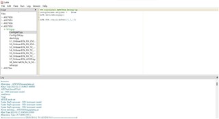
I made a ADC EVM ( AFE7950 ) similar to  AFE7950EVM

The difference is below:

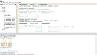
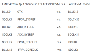
LMK04828 output channel in TI's AFE7950EVM   v.s.     ADC EVM I made

DCLK0          GTX                                                  v.s.           DCLK12

SDCLK1        FPGA_SYSREF                               v.s.           SDLCK13

DCLK2          ADC_REFCLK                                  v.s.           DCLK10

SDCLK3        ADC_SYSREF                                  v.s.          SDCLK11

SDCLK9        FPGA_REFCLK2                              v.s.          DCLK0

DCLK12         FPFA_CORECLK                             v.s.          SDCLK1

p.s. The rest is the same including TX, RX, SYNC.....

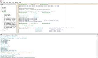
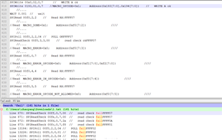
Here's my question: How can I modify the software latte so that the LMK04828 has the correct output

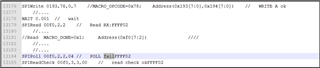
p.s. I tried to modify LMK output according to the E2E forum article

https://e2e.ti.com/support/rf-microwave-group/rf-microwave/f/rf-microwave-forum/1183600/afe7950evm-run-afe7950evm-on-htg-z920/4497259?tisearch=e2e-sitesearch&keymatch=afe7950#4497259

I found that it can only modify the LMK when I change the parameter in the LMK Clock Divider.

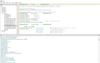
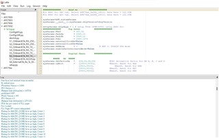
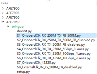
But once I run the script such as S1_OnboardCLK_RX_250M_TX_FB_500M.py

the LMK reset to previous setting so the ADC can't find the REFCLK !!

Pls help~ Thanks~

  • Hi Naiwen,

    What you can do is you split the programming of the AFE and LMK. This way you can program the LMK and make the adjustments that you need. Then you can program the AFE without affecting the LMK settings. The two scripts below can be used as a reference for splitting the programming. 

    ## Initiates AFE79xx Bring-up
    setupParams.skipLmk	=	True
    AFE.deviceBringup()
    
    AFE.TOP.overrideTdd(15,3,15)
    ##############		Read me			##############
    #In HSDC Pro DAC tab, Select AFE79xx_2x2TX_44210; Data Rate = 491.52M
    #In HSDC Pro ADC tab, Select AFE79xx_2x2RX_24410; Data Rate = 245.76M ---> To capture 4 RX channels
    #In HSDC Pro ADC tab, Select AFE79xx_1x2FB_44210; Data Rate = 491.52M ---> To capture 2 FB channels
    
    sysParams=AFE.systemParams
    sysParams.__init__();sysParams.chipVersion=chipVersion
    
    setupParams.skipFpga = 1 # setup FPGA (TSW14J56) using HSDC Pro 
    
    ##############		Top Level			##############
    sysParams.FRef			= 491.52
    sysParams.FadcRx		= 2949.12
    sysParams.FadcFb		= 2949.12
    sysParams.Fdac			= 2949.12*4
    sysParams.externalClockRx=False
    sysParams.externalClockTx=False
    													
    ##############		Digital Chain		##############
    
    		#####	RX	#####
    sysParams.ddcFactorRx	=	[12,12,12,12]			#DDC decimation factor for RX A, B, C and D
    sysParams.rxNco0		= 	[[9500,9500],			#Band0, Band1 for RXA 
    							[9500,9500],        	#Band0, Band1 for RXB 
    							[9500,9500],        	#Band0, Band1 for RXC 
    							[9500,9500]]        	#Band0, Band1 for RXD 
    
    		#####	FB	#####
    sysParams.ddcFactorFb	=	[6,6]					#DDC decimation factor for FB 1 and 2
    sysParams.fbNco0		= 	[9500,9500]				#Band0 for FB1 and FB2 
    
    		#####	TX	#####
    sysParams.ducFactorTx	=	[24,24,24,24]			#DUC interpolation factor for TX A, B, C and D
    sysParams.txNco0		= 	[[9500,9500],			#Band0, Band1 for TXA 
    							[9500,9500],        	#Band0, Band1 for TXB 
    							[9500,9500],        	#Band0, Band1 for TXC 
    							[9500,9500]]        	#Band0, Band1 for TXD
    
    
    ##############		JESD		##############
    
    		#####	ADC-JESD	#####
    sysParams.jesdSystemMode= [1,1]
    													#SystemMode 0:	2R1F-FDD						; rx1-rx2-fb -fb
    													#SystemMode 1:	1R1F-FDD						; rx -rx -fb -fb
    													#SystemMode 2:	2R-FDD							; rx1-rx1-rx2-rx2
    													#SystemMode 3:	1R								; rx -rx -rx -rx
    													#SystemMode 4:	1F								; fb -fb- fb -fb
    													#SystemMode 5:	1R1F-TDD						; rx/fb-rx/fb-rx/fb-rx/fb
    													
    sysParams.jesdTxProtocol= [0,0]						# 0 - 8b/10b encoding; 2 - 64b/66b encoding 
    sysParams.LMFSHdRx		= ["24410","24410","24410","24410"]
    													# The 2nd and 4th are valid only for jesdSystemMode values in (0,2).
    													# For other modes, select 4 converter modes for 1st and 3rd.
    sysParams.LMFSHdFb		= ["22210","22210"]
    
    sysParams.rxJesdTxScr	= [True,True,True,True]
    sysParams.fbJesdTxScr	= [True,True]
    
    sysParams.rxJesdTxK		= [16,16,16,16]
    sysParams.fbJesdTxK		= [16,16]
    
    sysParams.jesdTxLaneMux	= [0,1,2,3,4,5,6,7]			# Enter which lanes you want in each location. 
    													# For example, if you want to exchange the first two lines of each 2T,
    													#		this should be [[1,0,2,3],[5,4,6,7]]
    
    		#####	DAC-JESD	#####
    sysParams.jesdRxProtocol= [0,0]
    sysParams.LMFSHdTx		= ["44210","44210","44210","44210"]
    sysParams.jesdRxLaneMux	= [0,1,2,3,4,5,6,7]			# Enter which lanes you want in each location.
    													# For example, if you want to exchange the first two lines of each 2R
    													#		this should be [[1,0,2,3],[5,4,6,7]]
    sysParams.jesdRxRbd		= [4, 4]
    sysParams.jesdRxScr		= [True,True,True,True]
    sysParams.jesdRxK		= [16,16,16,16]
    
    		#####	JESD Common	#####
    	
    sysParams.jesdABLvdsSync= True
    sysParams.jesdCDLvdsSync= True
    sysParams.syncLoopBack	= True	#JESD Sync signal is connected to FPGA
    
    ##############		GPIO		##############
    sysParams.gpioMapping	= {
    						'H8': 'ADC_SYNC0',
    						'H7': 'ADC_SYNC1',
    						'N8': 'ADC_SYNC2',
    						'N7': 'ADC_SYNC3',
    						'H9': 'DAC_SYNC0',
    						'G9': 'DAC_SYNC1',
    						'N9': 'DAC_SYNC2',
    						'P9': 'DAC_SYNC3',
    						'P14': 'GLOBAL_PDN',
    						'K14': 'FBABTDD',
    						'R6': 'FBCDTDD',
    						'H15': ['TXATDD','TXBTDD'],
    						'V5': ['TXCTDD','TXDTDD'],
    						'E7': ['RXATDD','RXBTDD'],
    						'R15': ['RXCTDD','RXDTDD']}
    
    ##############		LMK Params		##############
    lmkParams.pllEn			= True
    lmkParams.inputClk		= 983.04 # Valid only when lmkParams.pllEn = False
    lmkParams.lmkFrefClk	= True
    setupParams.fpgaRefClk	= 245.76 # Should be equal to LaneRate/40 for TSW14J56
    
    ##############		Logging		##############
    logDumpInst.setFileName(ASTERIX_DIR+DEVICES_DIR+r"\Afe79xxPg1.txt")
    logDumpInst.logFormat=0x0 #Modify to 0x1 to save register scequence to log file. Script takes more time to execute.
    logDumpInst.rewriteFile=1
    logDumpInst.rewriteFileFormat4=1
    device.optimizeWrites=0
    device.rawWriteLogEn=1
    
    device.delay_time = 0
    #-------------------------------------------------------------------------------------------------#
    setupParams.skipLmk	=	False
    AFE.initializeConfig()
    lmkParams.sysrefFreq = AFE.systemStatus.sysrefFreq
    lmkParams.lmkPulseSysrefMode = False
    AFE.LMK.lmkConfig()

    Regards,

    David Chaparro

  • Hi David,

    Thanks for help !

    I follow your suggestion splitting the programming of the AFE and LMK

    It seems that LMK can output the correct channel so that the ADC can get the right REFCLK.

    However I encounter the next problem:

    the machine seems not to get MACRO_DOWN bit to go high

    Here is the screenshot for latte program:

    step1: setup.py

    step2: devinit.py

    step3: ConfigLMK.py

    and then I use the LMK Clock Divider setting the correct LMK output ( Checked by oscilloscope )

    step4: ConfigAFE.py

    It turns out to be the loop of wait for MACRO_DOWN bit to go high..........

    Please help, thanks

  • Hi Naiwen,

    This error may still be because of the clock. Can you confirm that the AFE is receiving the correct frequency for its RefClk, 491.52MHz? Also, can you share the LMK settings that you are using for the AFE reference clock output. 

    Regards,

    David Chaparro 

  • Hi David,

    Following attachment is log generated by latte and labview.

    In the labview log, the 1st error correspond to the OPCODE=0x1 and the 2nd error correspond to the OPCODE=0X78.

    In what circumstance will it cause the OPCODE=0x1 and OPCODE=0X78 ?

    Where can I find the document about these OPCODE ?

    Thanks~

    Afe79xxPg1_0217.txtLabview log.txt

  • Hi David,

    I have the another question: 

    Because I only need the function ADC of AFE7950, there is no RX and SYNCOUT on my ADC board design.

    Is it OK if I run the bring up S1_OnboardClk_RX_250M_TX_FB_500M that AFE7950 is used as a ADC only ?

    Or it will make the JESD connection between AFE and FPGA fail, because I discard the RX and SYNCOUT.

    thanks for help~

  • Here is the LMK settings~

  • Hi Naiwen,

    You can still use this script but you will receive the DAC JESD errors after the AFE configuration. To fix this you can disable the DACs by adding the following line, sysParams.txEnable = [False,False,False,False], before the AFE.deviceBringup() command. 

    The opcodes correspond to a certain Macro command that will be executed internally. Once the macro has completed a bit will be set to '1' indicating you can move on to the next step in the programming sequence. The issue that you are having is that when you are polling the macro done bit it never gets set to '1', which indicates that there is some error. Information on the opcodes and macros can be found in the Register Set document, SBAU337, which is available in the AFE79xx secure folder.

    One thing that can be tried on the AFE ref clock is to change the output format to LCPECL. This will make sure that the reference clock has a enough swing for the AFE input. 

    Regards,

    David Chaparro.

  • It seems that the error OPCODE is caused by RX data from FPGA~

    After closing the DACs, the latte software can run successfully.

    Thanks !