- Ask a related questionWhat is a related question?A related question is a question created from another question. When the related question is created, it will be automatically linked to the original question.
This thread has been locked.
If you have a related question, please click the "Ask a related question" button in the top right corner. The newly created question will be automatically linked to this question.
Part Number: TRF1208-AFE7950EVM
Tool/software:
Hi
I am taking the first steps to master the AFE7950 using the TSW14J57EVM using the AFE7950+TSW14J57.pptx method.
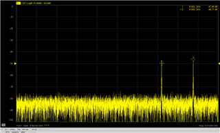
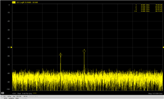
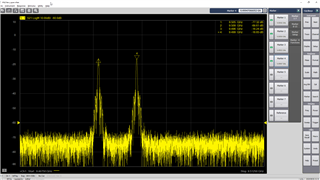
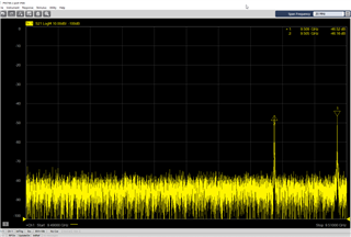
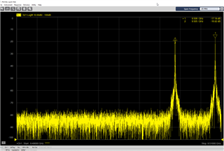
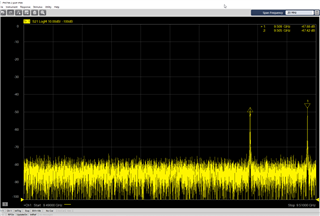
At step 5, instead of one harmonic at a frequency of (9500+9.9525) MHz, I see two harmonics at frequencies 9505 and 9509 MHz. What causes the harmonic at 9505 MHz?
There are no problems with powering the devices: directly on the AFE7950EVM board 5.1 V (current 3.7 A), directly on the TSW14J57EVM board 12.1 V (current 1.8 A).
I am attaching explanatory screenshots and logLatte.
Thanks in advance, Andrey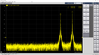
#======
#Executing .. AFE7950/bringup/setup.py
#Start Time 2024-06-18 11:35:38.878000
AFE79xxLibraryPG1p0
spi - USB Instrument created.
resetDevice
Kintex RegProgrammer - USB Instrument created.
Kintex RegProgrammer - USB Instrument created.
Kintex RegProgrammer - USB Instrument created.
#Done executing .. AFE7950/bringup/setup.py
#End Time 2024-06-18 11:35:48.111000
#Execution Time = 9.23300004005 s
#================ ERRORS:0, WARNINGS:0 ================#
#======
#Executing .. AFE7950/bringup/devInit.py
#Start Time 2024-06-18 11:39:22.260000
Power Card - USB Instrument created.
Reset the FPGA and try again.
Loaded Libraries
Refreshed GUI
#Done executing .. AFE7950/bringup/devInit.py
#End Time 2024-06-18 11:40:48.178000
#Execution Time = 85.9179999828 s
#================ ERRORS:1, WARNINGS:0 ================#
#======
#Executing .. AFE7950/bringup/S1_OnboardClk_RX_250M_TX_FB_500M.py
#Start Time 2024-06-18 11:45:28.578000
The External Sysref Frequency should be an integer factor of: 3.84MHz
2T2R1F Number: 0
Valid Configuration: True
laneRateRx: 9830.4
laneRateFb: 9830.4
laneRateTx: 9830.4
2T2R1F Number: 1
Valid Configuration: True
laneRateRx: 9830.4
laneRateFb: 9830.4
laneRateTx: 9830.4
LMK Clock Divider - Device registers reset.
LMK Clock Divider - Device registers reset.
REFCLOCK is used from LMK source, ensure board connections are ok to do the same
LMK and FPGA Configured.
DONOT_OPEN_Atharv_FULL - Device registers reset.
chipType: 0xa
chipId: 0x78
chipVersion: 0x11
AFE Reset Done
Fuse farm load autoload done successful
No autload error
Fuse farm load autoload done successful
No autload error
AFE MCU Wake up done and patch loaded.
PLL Locked
AFE PLL Configured.
AFE SerDes Configured.
AFE Digital Chains configured.
AFE TX Analog configured.
AFE RX Analog configured.
AFE FB Analog configured.
AFE JESD configured.
AFE AGC configured.
AFE GPIO configured.
Sysref Read as expected
###########Device DAC JESD-RX 0 Link Status###########
Serdes-FIFO error for lane 0: 1
Serdes-FIFO error for lane 1: 1
Serdes-FIFO error for lane 2: 1
Serdes-FIFO error for lane 3: 1
Comma Align Lock Lane0: False; Please check if the transmitter is sending data and eye is good.
Comma Align Lock Lane1: False; Please check if the transmitter is sending data and eye is good.
Comma Align Lock Lane2: False; Please check if the transmitter is sending data and eye is good.
Comma Align Lock Lane3: False; Please check if the transmitter is sending data and eye is good.
CS State TX0: 0b00000000 . It is expected to be 0b10101010
FS State TX0: 0b00000000 . It is expected to be 0b01010101
Couldn't get the link up for device RX: 0; Alarms: 0xf000
###################################
###########Device DAC JESD-RX 1 Link Status###########
Serdes-FIFO error for lane 0: 1
Serdes-FIFO error for lane 1: 1
Serdes-FIFO error for lane 2: 1
Serdes-FIFO error for lane 3: 1
Comma Align Lock Lane0: False; Please check if the transmitter is sending data and eye is good.
Comma Align Lock Lane1: False; Please check if the transmitter is sending data and eye is good.
Comma Align Lock Lane2: False; Please check if the transmitter is sending data and eye is good.
Comma Align Lock Lane3: False; Please check if the transmitter is sending data and eye is good.
CS State TX0: 0b00000000 . It is expected to be 0b10101010
FS State TX0: 0b00000000 . It is expected to be 0b01010101
Couldn't get the link up for device RX: 1; Alarms: 0xf000
###################################
AFE Configuration Complete
#Done executing .. AFE7950/bringup/S1_OnboardClk_RX_250M_TX_FB_500M.py
#End Time 2024-06-18 11:46:08.822000
#Execution Time = 40.243999958 s
#================ ERRORS:18, WARNINGS:1 ================#
###########Device DAC JESD-RX 0 Link Status###########
CS State TX0: 0b10101010 . It is expected to be 0b10101010
FS State TX0: 0b01010101 . It is expected to be 0b01010101
Could get the link up for device RX: 0
###################################
###########Device DAC JESD-RX 1 Link Status###########
CS State TX0: 0b10101010 . It is expected to be 0b10101010
FS State TX0: 0b01010101 . It is expected to be 0b01010101
Could get the link up for device RX: 1
###################################
#======
Hi Andrey,
I suspect that this issue would be caused by an incorrect setting on the HSDC Pro side, such as an issue with the ini file. Can you confirm that you are following the AFE79xx bringup guide for the TSW14J57 that is available in the AFE79xx secure folder? If not I would recommend to try the mode outlined and see if that fixes the spur issue. The bringup guide will have the settings for HSDC Pro and outline the required bringup procedure.
Regards,
David Chaparro

Hi David,
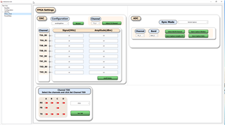
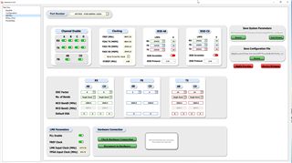
I indicated that I used the instructions AFE7950+TSW14J57.pptx, which was obtained from the AFE79xx_Bringup_Guides.zip archive. There is a very simple procedure for configuring FPGA, AFE and LMC on pages 6 and 7.
If you have some other instructions in mind, then please indicate the exact name of the required file, which is located in a protected folder. I didn't find anything else like it there.
Regards,
Andrey
Hi Andrey,
If the ppt was taken from the AFE79xx_Bringup_Guides.zip archive then that is the correct one. My suspect would then be on the ini file in HSDC Pro. Is this issue seen across all Tx channels.
Can you take a look at the ini file settings and confirm that they match the attached file? (Ini file can be found at the following location: C:\Program Files\Texas Instruments\High Speed Data Converter Pro\14J57revE Details\DAC files)
One additional test to verify if it is related to the tone send by the FPGA is to configure the DAC into a NCO test pattern mode using the writes given below.
enable=1
for i in range(4):
	CAFE.dacJesdConstantTestPatternEnable(0,i,enable)
	CAFE.dacJesdConstantTestPatternValue(0,i,0,0,35536) #0, chNo, bandNo, valueI, valueQ
Regards,
David Chaparro
Thank you, David.
The day after tomorrow I will check the contents of the specified ini file on my work computer.
Regarding the code:
enable=1
for i in range(4):
CAFE.dacJesdConstantTestPatternEnable(0,i,enable)
CAFE.dacJesdConstantTestPatternValue(0,i,0,0,35536) #0, chNo, bandNo, valueI, valueQ
Where should it be entered, in the Latte command line?
And what should be the result?
Regards,
Andrey
Hi Andrey,
I would suggest creating a seperate script for the code and run the script when testing the DAC in the NCO only mode. When you run those lines the DAC will be configured to output the NCO frequency directly, ignoring the data from the FPGA. So you should see a CW tone at the NCO frequency.
Regards,
David Chaparro
Hello David.
The INI files are identical.
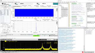
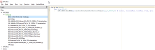
After the usual procedure, running the file S1_OnboardClk_RX_250M_TX_FB_500MT.py, I again got two harmonics instead of one. Then I ran your 4-line code in Latte as a py-file. But apparently I didn’t make this file correctly, because Latte threw an error and nothing in the spectrum changed. Here is Latte's log.
#================ ERRORS:1, WARNINGS:0 ================#
#======
#Executing .. AFE7950/bringup/S1_OnboardClk_RX_250M_TX_FB_500M.py
#Start Time 2024-06-23 12:00:59.503000
The External Sysref Frequency should be an integer factor of: 3.84MHz
2T2R1F Number: 0
Valid Configuration: True
laneRateRx: 9830.4
laneRateFb: 9830.4
laneRateTx: 9830.4
2T2R1F Number: 1
Valid Configuration: True
laneRateRx: 9830.4
laneRateFb: 9830.4
laneRateTx: 9830.4
LMK Clock Divider - Device registers reset.
LMK Clock Divider - Device registers reset.
REFCLOCK is used from LMK source, ensure board connections are ok to do the same
LMK and FPGA Configured.
DONOT_OPEN_Atharv_FULL - Device registers reset.
chipType: 0xa
chipId: 0x78
chipVersion: 0x11
AFE Reset Done
Fuse farm load autoload done successful
No autload error
Fuse farm load autoload done successful
No autload error
AFE MCU Wake up done and patch loaded.
PLL Locked
AFE PLL Configured.
AFE SerDes Configured.
AFE Digital Chains configured.
AFE TX Analog configured.
AFE RX Analog configured.
AFE FB Analog configured.
AFE JESD configured.
AFE AGC configured.
AFE GPIO configured.
Sysref Read as expected
###########Device DAC JESD-RX 0 Link Status###########
CS State TX0: 0b10101010 . It is expected to be 0b10101010
FS State TX0: 0b01010101 . It is expected to be 0b01010101
Could get the link up for device RX: 0
###################################
###########Device DAC JESD-RX 1 Link Status###########
CS State TX0: 0b10101010 . It is expected to be 0b10101010
FS State TX0: 0b01010101 . It is expected to be 0b01010101
Could get the link up for device RX: 1
###################################
AFE Configuration Complete
#Done executing .. AFE7950/bringup/S1_OnboardClk_RX_250M_TX_FB_500M.py
#End Time 2024-06-23 12:01:41.530000
#Execution Time = 42.0269999504 s
#================ ERRORS:0, WARNINGS:1 ================#
#======
#Executing .. AFE7950/bringup/DAC in the NCO only mode.py
#Start Time 2024-06-23 12:02:14.404000
#Error: afeCTestWrapper instance has no attribute 'dacJesdConstantTestPatternEnable'
# "AFE7950/bringup/DAC in the NCO only mode.py", line 3, in
# AttributeError: afeCTestWrapper instance has no attribute 'dacJesdConstantTestPatternEnable'
#
#
#Done executing .. AFE7950/bringup/DAC in the NCO only mode.py
#End Time 2024-06-23 12:02:14.413000
#Execution Time = 0.0090000629425 s
#================ ERRORS:1, WARNINGS:0 ================#
Regards,
Andrey
Hi Andrey,
Please try the updated lines below for NCO only mode.
for i in [0,1]:
	for j in [0,1]:
		AFE.JESD.DACJESD[i].dacJesdConstantTestPatternValue(1,j,0,35536,0) # enable, channelNum, bandNum, Ival, Qval
On the TSW14J57 can you report the status of the LEDs?
Regards,
David Chaparro
Hi David,
I tried running the updated lines for NCO only mode.
I am attaching screenshots of “before”, “after” and windows with this code. As you can see, the result does not meet expectations. In addition, the spectrum became dirtier than it previously was during my previous treatment.
The voltages directly on the boards are 12.2 V (current 1.8 A) and 5.1 V (current 3.7 A).
LED status on TSW14J57:
D1 - lights up or not (can change each time you press the SEND button);
D2 - started blinking only after the combination was launched (S1_OnboardClk_RX_250M_TX_FB_500M, AFE.adcDacSync(), SEND, SEND). It didn’t shine before;
D3 - always shines;
D4 - does not shine;
D5 - initially it shone brightly, but after launching S1_OnboardClk_RX_250M_TX_FB_500M it began to shine dimly;
D6 - shines;
D7 - does not shine;
D8 and D9 - always shine;
D10,11,13,14,15,17,18,19 (blue) - shine;
D16,22 - do not shine.
Sincerely,
Andrey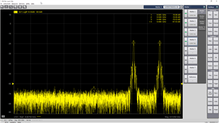
Hi Andrew,
The spectrum that you are seeing is not expected. Is this same issue seen on all channels or is it isolated to a single channel?
If you lower the amplitude of the output tone do you see any changes in the spectrum? To do this in the NCO only mode you can change the ‘35536’ to ‘8192’ in the function provided previously.
Regards,
David Chaparro
Hello David!
All channels behave the same.
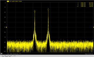
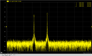
However, the harmonic amplitudes in the ТхВ and ТхД channels are lower than the amplitudes in the ТхА and ТхС channels by approximately 20 dB at the same noise level.
In the "NCD only" mode, the spectra are simply shifted to the left by 9.5 MHz.
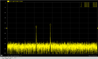
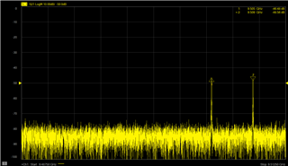
When moving from a value of 35336 to a value of 8192, the harmonic amplitudes in all channels decrease by approximately 10 dB while maintaining the same noise level.
David, the problem is not being solved. If you have no idea how to fix it, maybe your company will provide us with another, working kit?
Best wishes, Andrey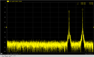
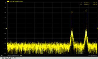
The pictures are arranged in the following order:
TxA,B,C,D after the standard script S1_OnboardClk_RX_250M_TX_FB_500M.py.
Then TxA,B in the “NCO only” mode with parameter 35336.
Then TxA,B in the “NCO only” mode with parameter 8192.
Hi Andrey,
Based on the fact that the issue is seen in NCO only configuration then the issue is either with the AFE configuration or the EVM hardware. One suggestion would be to try a different configuration on the AFE. Can you test the S3 configuration script?
Additionally, has the script S1 been modified in any way?
Regards,
David Chaparro
Hi David.
No, I did not change the S1 script, which should be clear from the Latte log that I posted here on June 23rd.
To begin with, I would like everything to work correctly with S1, as it is written in your instructions AFE7950+TSW14J57.pptx. I thought that I could master this platform using ready-made examples, and then quickly implement the functions I needed based on them, since I do not yet have time to independently understand the command system and register model of the AFE7950.
But I can try S3 too. At the same time, I need a priori information, what should I expect on the spectrum analyzer, following the example of the above instructions?
And even better, if you have instructions for detailed equipment diagnostics, I can immediately quickly collect all the information for your analysis, so as not to delay the solution to the problem.
Best wishes, Andrey
Hi David.
I looked at the S3 script. As I see, in terms of the transmitter it is no different from S1.
The results are also similar. I am attaching screenshots of TxA,B,C,D and logs.
With all respect, Andrey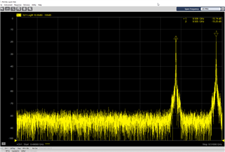
#======
#Executing .. AFE7950/bringup/setup.py
#Start Time 2024-07-14 12:00:07.093000
AFE79xxLibraryPG1p0
spi - USB Instrument created.
resetDevice
Kintex RegProgrammer - USB Instrument created.
Kintex RegProgrammer - USB Instrument created.
Kintex RegProgrammer - USB Instrument created.
#Done executing .. AFE7950/bringup/setup.py
#End Time 2024-07-14 12:00:14.865000
#Execution Time = 7.77200007439 s
#================ ERRORS:0, WARNINGS:0 ================#
#======
#Executing .. AFE7950/bringup/devInit.py
#Start Time 2024-07-14 12:00:27.686000
Power Card - USB Instrument created.
Reset the FPGA and try again.
Loaded Libraries
Refreshed GUI
#Done executing .. AFE7950/bringup/devInit.py
#End Time 2024-07-14 12:01:52.234000
#Execution Time = 84.5479998589 s
#================ ERRORS:1, WARNINGS:0 ================#
#======
#Executing .. AFE7950/bringup/S3_OnboardClk_RX_TX_500M_FB_disabled.py
#Start Time 2024-07-14 12:05:31.841000
The External Sysref Frequency should be an integer factor of: 5.12MHz
2T2R1F Number: 0
Valid Configuration: True
laneRateRx: 9830.4
laneRateFb: 9830.4
laneRateTx: 9830.4
2T2R1F Number: 1
Valid Configuration: True
laneRateRx: 9830.4
laneRateFb: 9830.4
laneRateTx: 9830.4
LMK Clock Divider - Device registers reset.
LMK Clock Divider - Device registers reset.
REFCLOCK is used from LMK source, ensure board connections are ok to do the same
LMK and FPGA Configured.
DONOT_OPEN_Atharv_FULL - Device registers reset.
chipType: 0xa
chipId: 0x78
chipVersion: 0x11
AFE Reset Done
Fuse farm load autoload done successful
No autload error
Fuse farm load autoload done successful
No autload error
AFE MCU Wake up done and patch loaded.
PLL Locked
AFE PLL Configured.
AFE SerDes Configured.
AFE Digital Chains configured.
AFE TX Analog configured.
AFE RX Analog configured.
AFE FB Analog configured.
AFE JESD configured.
AFE AGC configured.
AFE GPIO configured.
Sysref Read as expected
###########Device DAC JESD-RX 0 Link Status###########
Serdes-FIFO error for lane 0: 1
Serdes-FIFO error for lane 1: 1
Serdes-FIFO error for lane 2: 1
Serdes-FIFO error for lane 3: 1
Comma Align Lock Lane0: False; Please check if the transmitter is sending data and eye is good.
Comma Align Lock Lane1: False; Please check if the transmitter is sending data and eye is good.
Comma Align Lock Lane2: False; Please check if the transmitter is sending data and eye is good.
Comma Align Lock Lane3: False; Please check if the transmitter is sending data and eye is good.
CS State TX0: 0b00000000 . It is expected to be 0b10101010
FS State TX0: 0b00000000 . It is expected to be 0b01010101
Couldn't get the link up for device RX: 0; Alarms: 0xf000
###################################
###########Device DAC JESD-RX 1 Link Status###########
Serdes-FIFO error for lane 0: 1
Serdes-FIFO error for lane 1: 1
Serdes-FIFO error for lane 2: 1
Serdes-FIFO error for lane 3: 1
Comma Align Lock Lane0: False; Please check if the transmitter is sending data and eye is good.
Comma Align Lock Lane1: False; Please check if the transmitter is sending data and eye is good.
Comma Align Lock Lane2: False; Please check if the transmitter is sending data and eye is good.
Comma Align Lock Lane3: False; Please check if the transmitter is sending data and eye is good.
CS State TX0: 0b00000000 . It is expected to be 0b10101010
FS State TX0: 0b00000000 . It is expected to be 0b01010101
Couldn't get the link up for device RX: 1; Alarms: 0xf000
###################################
AFE Configuration Complete
#Done executing .. AFE7950/bringup/S3_OnboardClk_RX_TX_500M_FB_disabled.py
#End Time 2024-07-14 12:06:11.183000
#Execution Time = 39.3420000076 s
#================ ERRORS:18, WARNINGS:1 ================#
###########Device DAC JESD-RX 0 Link Status###########
Serdes-FIFO error for lane 0: 1
Serdes-FIFO error for lane 1: 1
Serdes-FIFO error for lane 2: 1
Serdes-FIFO error for lane 3: 1
Comma Align Lock Lane0: False; Please check if the transmitter is sending data and eye is good.
Comma Align Lock Lane1: False; Please check if the transmitter is sending data and eye is good.
Comma Align Lock Lane2: False; Please check if the transmitter is sending data and eye is good.
Comma Align Lock Lane3: False; Please check if the transmitter is sending data and eye is good.
CS State TX0: 0b00000000 . It is expected to be 0b10101010
FS State TX0: 0b00000000 . It is expected to be 0b01010101
Couldn't get the link up for device RX: 0; Alarms: 0xf000
###################################
###########Device DAC JESD-RX 1 Link Status###########
Serdes-FIFO error for lane 0: 1
Serdes-FIFO error for lane 1: 1
Serdes-FIFO error for lane 2: 1
Serdes-FIFO error for lane 3: 1
Comma Align Lock Lane0: False; Please check if the transmitter is sending data and eye is good.
Comma Align Lock Lane1: False; Please check if the transmitter is sending data and eye is good.
Comma Align Lock Lane2: False; Please check if the transmitter is sending data and eye is good.
Comma Align Lock Lane3: False; Please check if the transmitter is sending data and eye is good.
CS State TX0: 0b00000000 . It is expected to be 0b10101010
FS State TX0: 0b00000000 . It is expected to be 0b01010101
Couldn't get the link up for device RX: 1; Alarms: 0xf000
###################################
#======
###########Device DAC JESD-RX 0 Link Status###########
CS State TX0: 0b10101010 . It is expected to be 0b10101010
FS State TX0: 0b01010101 . It is expected to be 0b01010101
Could get the link up for device RX: 0
###################################
###########Device DAC JESD-RX 1 Link Status###########
CS State TX0: 0b10101010 . It is expected to be 0b10101010
FS State TX0: 0b01010101 . It is expected to be 0b01010101
Could get the link up for device RX: 1
###################################
#======
Qt: Untested Windows version 10.0 detected! [Errno 13] Permission denied: u'C:\\Users\\andreysheleg\\Documents\\Texas Instruments\\AFE79xxLatte\\projects\\/temp/AFE7900/bringup' [Errno 13] Permission denied: u'C:\\Users\\andreysheleg\\Documents\\Texas Instruments\\AFE79xxLatte\\projects\\/temp/AFE7901/bringup' [Errno 13] Permission denied: u'C:\\Users\\andreysheleg\\Documents\\Texas Instruments\\AFE79xxLatte\\projects\\/temp/AFE7903/bringup' [Errno 13] Permission denied: u'C:\\Users\\andreysheleg\\Documents\\Texas Instruments\\AFE79xxLatte\\projects\\/temp/AFE7906/bringup' [Errno 13] Permission denied: u'C:\\Users\\andreysheleg\\Documents\\Texas Instruments\\AFE79xxLatte\\projects\\/temp/AFE7951/bringup' [Errno 13] Permission denied: u'C:\\Users\\andreysheleg\\Documents\\Texas Instruments\\AFE79xxLatte\\projects\\/temp/AFE7953/bringup' [Errno 13] Permission denied: u'C:\\Users\\andreysheleg\\Documents\\Texas Instruments\\AFE79xxLatte\\projects\\/temp/AFE7954/bringup' [Errno 13] Permission denied: u'C:\\Users\\andreysheleg\\Documents\\Texas Instruments\\AFE79xxLatte\\projects\\/temp/AFE7955/bringup' [Errno 13] Permission denied: u'C:\\Users\\andreysheleg\\Documents\\Texas Instruments\\AFE79xxLatte\\projects\\/temp/TSW14J58/Scripts' u'' <string>:199: SyntaxWarning: import * only allowed at module level Connecting... 0 ERROR: Please check environment setup! No device is detected. FTDI Not Connected Opened the USB FTDI Handle. Closing the USB FTDI Handle. couldn't create image from "https://cdn4.iconfinder.com/data/icons/ionicons/512/icon-plus-round-128.png" couldn't create image from "https://cdn4.iconfinder.com/data/icons/essential-app-2/16/record-round-circle-dot-128.png" couldn't create image from "https://cdn4.iconfinder.com/data/icons/essential-app-2/16/record-round-circle-dot-128.png" couldn't create image from "https://cdn4.iconfinder.com/data/icons/essential-app-2/16/record-round-circle-dot-128.png" couldn't create image from "https://cdn4.iconfinder.com/data/icons/essential-app-2/16/record-round-circle-dot-128.png" couldn't create image from "https://cdn4.iconfinder.com/data/icons/essential-app-2/16/record-round-circle-dot-128.png" Writing into 0x0000 value 0x30 Writing into 0x0000 value 0xb0 Writing into 0x0000 value 0x30 Writing into 0x0000 value 0x30 Writing into 0x0000 value 0x30 Reading From 0x0003 value 0x0a Reading From 0x0004 value 0x78 Reading From 0x0005 value 0x00 Reading From 0x0006 value 0x11 Reading From 0x0007 value 0x51 Reading From 0x0008 value 0x04 Writing into 0x0015 value 0x80 Writing into 0x0191 value 0x00 Writing into 0x0231 value 0x00 Writing into 0x02d1 value 0x00 Writing into 0x0371 value 0x00 Writing into 0x042a value 0x00 Writing into 0x04e2 value 0x00 Writing into 0x059a value 0x00 Writing into 0x0652 value 0x00 Writing into 0x070a value 0x00 Writing into 0x07c2 value 0x00 Writing into 0x00ec value 0x01 Writing into 0x00f4 value 0x01 Writing into 0x00e4 value 0x01 Writing into 0x00ed value 0x00 Writing into 0x00f5 value 0x00 Writing into 0x00e5 value 0x00 Writing into 0x00ed value 0x00 Writing into 0x00f5 value 0x00 Writing into 0x00e5 value 0x00 Writing into 0x0015 value 0x00 Writing into 0x0015 value 0x40 Writing into 0x0190 value 0x03 Writing into 0x0190 value 0x01 Writing into 0x0015 value 0x00 Writing into 0x0015 value 0x40 Writing into 0x0931 value 0x01 Writing into 0x0931 value 0x03 Writing into 0x0015 value 0x00 Writing into 0x0011 value 0x3f Writing into 0x00ce value 0x20 Writing into 0x00cb value 0x04 Writing into 0x00ca value 0x20 Writing into 0x00ce value 0x30 Writing into 0x00c3 value 0x40 Writing into 0x00c0 value 0x01 Writing into 0x00b9 value 0x40 Writing into 0x00b9 value 0x50 Writing into 0x00b9 value 0x70 Writing into 0x00b9 value 0x78 Writing into 0x0011 value 0x00 Writing into 0x0010 value 0x3f Writing into 0x00b0 value 0x30 Writing into 0x00b4 value 0x30 Writing into 0x0010 value 0x00 Writing into 0x0015 value 0x02 Writing into 0x00c0 value 0x00 Writing into 0x0015 value 0x00 Writing into 0x0015 value 0x40 Writing into 0x0170 value 0x01 Writing into 0x0540 value 0x00 Reading From 0x0171 value 0x01 Writing into 0x0015 value 0x00 Writing into 0x0015 value 0x01 Writing into 0x0054 value 0x81 Writing into 0x0015 value 0x00 Writing into 0x0015 value 0x40 Writing into 0x0170 value 0x00 Writing into 0x0540 value 0x00 Writing into 0x0015 value 0x00 Writing into 0x0015 value 0x40 Writing into 0x08a8 value 0x02 Writing into 0x0810 value 0x01 Writing into 0x0830 value 0x01 Writing into 0x0200 value 0x00 Writing into 0x0210 value 0x00 Writing into 0x0814 value 0x00 Writing into 0x0834 value 0x00 Writing into 0x0814 value 0x01 Writing into 0x0834 value 0x01 Writing into 0x0810 value 0x00 Writing into 0x0830 value 0x00 Writing into 0x0810 value 0x01 Writing into 0x0830 value 0x01 Writing into 0x0200 value 0x05 Writing into 0x0210 value 0x00 Writing into 0x0814 value 0x03 Writing into 0x0834 value 0x03 Writing into 0x0814 value 0x00 Writing into 0x0834 value 0x00 Writing into 0x0810 value 0x00 Writing into 0x0830 value 0x00 Writing into 0x0814 value 0x00 Writing into 0x0834 value 0x00 Writing into 0x0814 value 0x1c Writing into 0x0834 value 0x1c Writing into 0x0814 value 0x00 Writing into 0x0834 value 0x00 Reading From 0x0150 value 0x0f Reading From 0x0150 value 0x0f Reading From 0x0160 value 0x0f Reading From 0x0160 value 0x0f Writing into 0x0830 value 0x01 Writing into 0x0810 value 0x01 Writing into 0x0910 value 0x0f Writing into 0x0911 value 0x03 Writing into 0x0912 value 0x0f Writing into 0x0015 value 0x00 Writing into 0x0016 value 0x10 Writing into 0x00c1 value 0x02 Writing into 0x00c0 value 0x42 Writing into 0x00c0 value 0x42 Writing into 0x00c0 value 0xc2 Writing into 0x00c0 value 0x42 Writing into 0x0016 value 0x00 Writing into 0x0018 value 0x20 Writing into 0x0140 value 0x01 Writing into 0x0140 value 0x00 Reading From 0x00f0 value 0x01 Writing into 0x00a3 value 0x00 Writing into 0x00a2 value 0x00 Writing into 0x00a1 value 0x00 Writing into 0x00a0 value 0x02 Writing into 0x0193 value 0x01 Reading From 0x00f0 value 0x07 Reading From 0x00f0 value 0x07 Reading From 0x00f1 value 0x00 Reading From 0x00f0 value 0x07 Reading From 0x00f0 value 0x07 Reading From 0x00f0 value 0x07 Reading From 0x00f0 value 0x07 Reading From 0x00f3 value 0x00 Reading From 0x00f2 value 0x00 Reading From 0x00f7 value 0x00 Reading From 0x00f6 value 0x00 Reading From 0x00f5 value 0x00 Reading From 0x00f4 value 0x00 Reading From 0x00fb value 0x13 Reading From 0x00fa value 0x07 Reading From 0x00f9 value 0x0a Reading From 0x00f8 value 0x01 Reading From 0x00ff value 0x00 Reading From 0x00fe value 0x00 Reading From 0x00fd value 0x2a Reading From 0x00fc value 0xf8 Reading From 0x00f0 value 0x07 Writing into 0x00a3 value 0x00 Writing into 0x00a2 value 0x00 Writing into 0x00a1 value 0x00 Writing into 0x00a0 value 0x00 Writing into 0x0193 value 0x90 Reading From 0x00f0 value 0x07 Reading From 0x00f0 value 0x07 Reading From 0x00f1 value 0x00 Reading From 0x00f0 value 0x07 Reading From 0x00f0 value 0x07 Reading From 0x00f0 value 0x07 Reading From 0x00f0 value 0x07 Reading From 0x00f3 value 0x00 Reading From 0x00f2 value 0x00 Reading From 0x00f7 value 0x00 Reading From 0x00f6 value 0x00 Reading From 0x00f5 value 0x00 Reading From 0x00f4 value 0x00 Writing into 0x0144 value 0x08 Writing into 0x0018 value 0x00 Writing into 0x0018 value 0x08 Writing into 0x1a28 value 0x10 Writing into 0x1a29 value 0x27 Writing into 0x1a2a value 0x00 Writing into 0x1a2b value 0x00 Writing into 0x0018 value 0x00 Writing into 0x0018 value 0x20 Writing into 0x0144 value 0x08 Writing into 0x0018 value 0x00 Writing into 0x0018 value 0x08 Writing into 0x1a2c value 0x10 Writing into 0x1a2d value 0x27 Writing into 0x1a2e value 0x00 Writing into 0x1a2f value 0x00 Writing into 0x0018 value 0x00 Writing into 0x0018 value 0x20 Writing into 0x0144 value 0x08 Writing into 0x0018 value 0x00 Writing into 0x0018 value 0x08 Writing into 0x1a30 value 0x10 Writing into 0x1a31 value 0x27 Writing into 0x1a32 value 0x00 Writing into 0x1a33 value 0x00 Writing into 0x0018 value 0x00 Writing into 0x0018 value 0x20 Writing into 0x0144 value 0x08 Writing into 0x0018 value 0x00 Writing into 0x0018 value 0x08 Writing into 0x1a34 value 0x10 Writing into 0x1a35 value 0x27 Writing into 0x1a36 value 0x00 Writing into 0x1a37 value 0x00 Writing into 0x0018 value 0x00 Writing into 0x0018 value 0x20 Writing into 0x0144 value 0x08 Writing into 0x0018 value 0x00 Writing into 0x0018 value 0x08 Writing into 0x03bf value 0x00 Writing into 0x03be value 0x07 Writing into 0x03bd value 0x80 Writing into 0x03bc value 0x00 Writing into 0x03c3 value 0x00 Writing into 0x03c2 value 0x04 Writing into 0x03c1 value 0x17 Writing into 0x03c0 value 0x46 Writing into 0x03d0 value 0x05 Writing into 0x03ac value 0x1d Writing into 0x03ad value 0x1d Writing into 0x1abd value 0x03 Writing into 0x1402 value 0x00 Writing into 0x1403 value 0x00 Writing into 0x1401 value 0x00 Writing into 0x0018 value 0x00 Writing into 0x0018 value 0x20 Writing into 0x0144 value 0x08 Writing into 0x0018 value 0x00 Writing into 0x0018 value 0x08 Writing into 0x1b5f value 0x0e Writing into 0x0018 value 0x00 Writing into 0x0018 value 0x20 Writing into 0x0144 value 0x08 Writing into 0x0018 value 0x00 Writing into 0x0018 value 0x08 Writing into 0x1b6f value 0x07 Writing into 0x0018 value 0x00 Writing into 0x0018 value 0x20 Writing into 0x0144 value 0x08 Writing into 0x0018 value 0x00 Writing into 0x0018 value 0x08 Writing into 0x1e7d value 0x07 Writing into 0x0018 value 0x00 Writing into 0x0018 value 0x20 Writing into 0x0144 value 0x08 Writing into 0x0018 value 0x00 Writing into 0x0018 value 0x08 Writing into 0x1a68 value 0x80 Writing into 0x1a69 value 0x05 Writing into 0x0018 value 0x00 Writing into 0x0018 value 0x20 Writing into 0x0144 value 0x08 Writing into 0x0018 value 0x00 Writing into 0x0018 value 0x08 Writing into 0x1b1e value 0x80 Writing into 0x1b1f value 0x05 Writing into 0x0018 value 0x00 Writing into 0x0018 value 0x20 Reading From 0x00f0 value 0x07 Writing into 0x00a3 value 0x00 Writing into 0x00a2 value 0x00 Writing into 0x00a1 value 0x00 Writing into 0x00a0 value 0x01 Writing into 0x0193 value 0x90 Reading From 0x00f0 value 0x07 Reading From 0x00f0 value 0x07 Reading From 0x00f1 value 0x00 Reading From 0x00f0 value 0x07 Reading From 0x00f0 value 0x07 Reading From 0x00f0 value 0x07 Reading From 0x00f0 value 0x07 Reading From 0x00f3 value 0x00 Reading From 0x00f2 value 0x00 Reading From 0x00f7 value 0x00 Reading From 0x00f6 value 0x00 Reading From 0x00f5 value 0x00 Reading From 0x00f4 value 0x00 Writing into 0x0018 value 0x00 Writing into 0x0018 value 0x20 Writing into 0x0144 value 0x00 Writing into 0x0018 value 0x00 Writing into 0x0018 value 0x01 Writing into 0x0018 value 0x00 Writing into 0x0018 value 0x20 Reading From 0x00f0 value 0x07 Writing into 0x00a3 value 0x08 Writing into 0x00a2 value 0x00 Writing into 0x00a1 value 0x00 Writing into 0x00a0 value 0x00 Writing into 0x00a7 value 0x00 Writing into 0x00a6 value 0x00 Writing into 0x00a5 value 0x00 Writing into 0x00a4 value 0x00 Writing into 0x0193 value 0x78 Reading From 0x00f0 value 0x07 Reading From 0x00f0 value 0x07 Reading From 0x00f1 value 0x00 Reading From 0x00f0 value 0x07 Reading From 0x00f0 value 0x07 Reading From 0x00f0 value 0x07 Reading From 0x00f0 value 0x07 Reading From 0x00f3 value 0x00 Reading From 0x00f2 value 0x00 Reading From 0x00f7 value 0x00 Reading From 0x00f6 value 0x00 Reading From 0x00f5 value 0x00 Reading From 0x00f4 value 0x00 Writing into 0x0144 value 0x00 Writing into 0x0018 value 0x00 Writing into 0x0018 value 0x01 Writing into 0x0018 value 0x00 Writing into 0x0018 value 0x20 Reading From 0x00f0 value 0x07 Writing into 0x00a3 value 0x08 Writing into 0x00a2 value 0x00 Writing into 0x00a1 value 0x00 Writing into 0x00a0 value 0x00 Writing into 0x00a7 value 0x00 Writing into 0x00a6 value 0x00 Writing into 0x00a5 value 0x08 Writing into 0x00a4 value 0x00 Writing into 0x0193 value 0x78 Reading From 0x00f0 value 0x07 Reading From 0x00f0 value 0x07 Reading From 0x00f1 value 0x00 Reading From 0x00f0 value 0x07 Reading From 0x00f0 value 0x07 Reading From 0x00f0 value 0x07 Reading From 0x00f0 value 0x07 Reading From 0x00f3 value 0x00 Reading From 0x00f2 value 0x00 Reading From 0x00f7 value 0x00 Reading From 0x00f6 value 0x00 Reading From 0x00f5 value 0x00 Reading From 0x00f4 value 0x00 Writing into 0x0144 value 0x00 Writing into 0x0018 value 0x00 Writing into 0x0018 value 0x01 Writing into 0x0018 value 0x00 Writing into 0x0018 value 0x20 Reading From 0x00f0 value 0x07 Writing into 0x00a3 value 0x08 Writing into 0x00a2 value 0x00 Writing into 0x00a1 value 0x00 Writing into 0x00a0 value 0x00 Writing into 0x00a7 value 0x00 Writing into 0x00a6 value 0x00 Writing into 0x00a5 value 0x10 Writing into 0x00a4 value 0x00 Writing into 0x0193 value 0x78 Reading From 0x00f0 value 0x07 Reading From 0x00f0 value 0x07 Reading From 0x00f1 value 0x00 Reading From 0x00f0 value 0x07 Reading From 0x00f0 value 0x07 Reading From 0x00f0 value 0x07 Reading From 0x00f0 value 0x07 Reading From 0x00f3 value 0x00 Reading From 0x00f2 value 0x00 Reading From 0x00f7 value 0x00 Reading From 0x00f6 value 0x00 Reading From 0x00f5 value 0x00 Reading From 0x00f4 value 0x00 Writing into 0x0144 value 0x00 Writing into 0x0018 value 0x00 Writing into 0x0018 value 0x01 Writing into 0x0018 value 0x00 Writing into 0x0018 value 0x20 Reading From 0x00f0 value 0x07 Writing into 0x00a3 value 0x08 Writing into 0x00a2 value 0x00 Writing into 0x00a1 value 0x00 Writing into 0x00a0 value 0x00 Writing into 0x00a7 value 0x00 Writing into 0x00a6 value 0x00 Writing into 0x00a5 value 0x18 Writing into 0x00a4 value 0x00 Writing into 0x0193 value 0x78 Reading From 0x00f0 value 0x07 Reading From 0x00f0 value 0x07 Reading From 0x00f1 value 0x00 Reading From 0x00f0 value 0x07 Reading From 0x00f0 value 0x07 Reading From 0x00f0 value 0x07 Reading From 0x00f0 value 0x07 Reading From 0x00f3 value 0x00 Reading From 0x00f2 value 0x00 Reading From 0x00f7 value 0x00 Reading From 0x00f6 value 0x00 Reading From 0x00f5 value 0x00 Reading From 0x00f4 value 0x00 Writing into 0x0144 value 0x00 Writing into 0x0018 value 0x00 Writing into 0x0018 value 0x01 Writing into 0x0018 value 0x00 Writing into 0x0018 value 0x20 Reading From 0x00f0 value 0x07 Writing into 0x00a3 value 0x08 Writing into 0x00a2 value 0x00 Writing into 0x00a1 value 0x00 Writing into 0x00a0 value 0x00 Writing into 0x00a7 value 0x00 Writing into 0x00a6 value 0x00 Writing into 0x00a5 value 0x20 Writing into 0x00a4 value 0x00 Writing into 0x0193 value 0x78 Reading From 0x00f0 value 0x07 Reading From 0x00f0 value 0x07 Reading From 0x00f1 value 0x00 Reading From 0x00f0 value 0x07 Reading From 0x00f0 value 0x07 Reading From 0x00f0 value 0x07 Reading From 0x00f0 value 0x07 Reading From 0x00f3 value 0x00 Reading From 0x00f2 value 0x00 Reading From 0x00f7 value 0x00 Reading From 0x00f6 value 0x00 Reading From 0x00f5 value 0x00 Reading From 0x00f4 value 0x00 Writing into 0x0144 value 0x00 Writing into 0x0018 value 0x00 Writing into 0x0018 value 0x01 Writing into 0x0018 value 0x00 Writing into 0x0018 value 0x20 Reading From 0x00f0 value 0x07 Writing into 0x00a3 value 0x08 Writing into 0x00a2 value 0x00 Writing into 0x00a1 value 0x00 Writing into 0x00a0 value 0x00 Writing into 0x00a7 value 0x00 Writing into 0x00a6 value 0x00 Writing into 0x00a5 value 0x28 Writing into 0x00a4 value 0x00 Writing into 0x0193 value 0x78 Reading From 0x00f0 value 0x07 Reading From 0x00f0 value 0x07 Reading From 0x00f1 value 0x00 Reading From 0x00f0 value 0x07 Reading From 0x00f0 value 0x07 Reading From 0x00f0 value 0x07 Reading From 0x00f0 value 0x07 Reading From 0x00f3 value 0x00 Reading From 0x00f2 value 0x00 Reading From 0x00f7 value 0x00 Reading From 0x00f6 value 0x00 Reading From 0x00f5 value 0x00 Reading From 0x00f4 value 0x00 Writing into 0x0144 value 0x00 Writing into 0x0018 value 0x00 Writing into 0x0018 value 0x01 Writing into 0x0018 value 0x00 Writing into 0x0018 value 0x20 Reading From 0x00f0 value 0x07 Writing into 0x00a3 value 0x00 Writing into 0x00a2 value 0x71 Writing into 0x00a1 value 0x00 Writing into 0x00a0 value 0x00 Writing into 0x00a7 value 0x00 Writing into 0x00a6 value 0x00 Writing into 0x00a5 value 0x30 Writing into 0x00a4 value 0x00 Writing into 0x0193 value 0x78 Reading From 0x00f0 value 0x07 Reading From 0x00f0 value 0x07 Reading From 0x00f1 value 0x00 Reading From 0x00f0 value 0x07 Reading From 0x00f0 value 0x07 Reading From 0x00f0 value 0x07 Reading From 0x00f0 value 0x07 Reading From 0x00f3 value 0x00 Reading From 0x00f2 value 0x00 Reading From 0x00f7 value 0x00 Reading From 0x00f6 value 0x00 Reading From 0x00f5 value 0x00 Reading From 0x00f4 value 0x00 Reading From 0x00f0 value 0x07 Writing into 0x00a3 value 0x00 Writing into 0x00a2 value 0x00 Writing into 0x00a1 value 0x00 Writing into 0x00a0 value 0x01 Writing into 0x0193 value 0x78 Reading From 0x00f0 value 0x07 Reading From 0x00f0 value 0x07 Reading From 0x00f1 value 0x00 Reading From 0x00f0 value 0x07 Reading From 0x00f0 value 0x07 Reading From 0x00f0 value 0x07 Reading From 0x00f0 value 0x07 Reading From 0x00f3 value 0x00 Reading From 0x00f2 value 0x00 Reading From 0x00f7 value 0x00 Reading From 0x00f6 value 0x00 Reading From 0x00f5 value 0x00 Reading From 0x00f4 value 0x00 Reading From 0x00f0 value 0x07 Writing into 0x00a3 value 0x00 Writing into 0x00a2 value 0x00 Writing into 0x00a1 value 0x00 Writing into 0x00a0 value 0x03 Writing into 0x0193 value 0x01 Reading From 0x00f0 value 0x07 Reading From 0x00f0 value 0x07 Reading From 0x00f1 value 0x00 Reading From 0x00f0 value 0x07 Reading From 0x00f0 value 0x07 Reading From 0x00f0 value 0x07 Reading From 0x00f0 value 0x07 Reading From 0x00f3 value 0x00 Reading From 0x00f2 value 0x00 Reading From 0x00f7 value 0x00 Reading From 0x00f6 value 0x00 Reading From 0x00f5 value 0x00 Reading From 0x00f4 value 0x00 Reading From 0x00fb value 0x17 Reading From 0x00fa value 0x0a Reading From 0x00f9 value 0x0d Reading From 0x00f8 value 0x00 Reading From 0x00ff value 0x00 Reading From 0x00fe value 0x00 Reading From 0x00fd value 0x00 Reading From 0x00fc value 0xa9 Writing into 0x0018 value 0x00 Writing into 0x0015 value 0x02 Writing into 0x00c0 value 0x80 Writing into 0x0015 value 0x00 Writing into 0x0015 value 0x40 Writing into 0x02a3 value 0x00 Writing into 0x02a2 value 0x00 Writing into 0x02a1 value 0x00 Writing into 0x02a0 value 0x7e Writing into 0x02a7 value 0x01 Writing into 0x02a6 value 0x00 Writing into 0x02a5 value 0x00 Writing into 0x02a4 value 0x00 Writing into 0x0015 value 0x00 Writing into 0x0018 value 0x20 Reading From 0x00f0 value 0x07 Writing into 0x00a3 value 0x00 Writing into 0x00a2 value 0x00 Writing into 0x00a1 value 0x02 Writing into 0x00a0 value 0x0f Writing into 0x0193 value 0x34 Reading From 0x00f0 value 0x07 Reading From 0x00f0 value 0x07 Reading From 0x00f1 value 0x00 Reading From 0x00f0 value 0x07 Reading From 0x00f0 value 0x07 Reading From 0x00f0 value 0x07 Reading From 0x00f0 value 0x07 Reading From 0x00f3 value 0x00 Reading From 0x00f2 value 0x00 Reading From 0x00f7 value 0x00 Reading From 0x00f6 value 0x00 Reading From 0x00f5 value 0x00 Reading From 0x00f4 value 0x00 Reading From 0x00f0 value 0x07 Writing into 0x00a3 value 0x00 Writing into 0x00a2 value 0x00 Writing into 0x00a1 value 0x00 Writing into 0x00a0 value 0x01 Writing into 0x0193 value 0x72 Reading From 0x00f0 value 0x07 Reading From 0x00f0 value 0x07 Reading From 0x00f1 value 0x00 Reading From 0x00f0 value 0x07 Reading From 0x00f0 value 0x07 Reading From 0x00f0 value 0x07 Reading From 0x00f0 value 0x07 Reading From 0x00f3 value 0x00 Reading From 0x00f2 value 0x00 Reading From 0x00f7 value 0x00 Reading From 0x00f6 value 0x00 Reading From 0x00f5 value 0x00 Reading From 0x00f4 value 0x00 Reading From 0x00f0 value 0x07 Writing into 0x00a3 value 0x00 Writing into 0x00a2 value 0x0e Writing into 0x00a1 value 0x01 Writing into 0x00a0 value 0x00 Writing into 0x0193 value 0x71 Reading From 0x00f0 value 0x07 Reading From 0x00f0 value 0x07 Reading From 0x00f1 value 0x00 Reading From 0x00f0 value 0x07 Reading From 0x00f0 value 0x07 Reading From 0x00f0 value 0x07 Reading From 0x00f0 value 0x07 Reading From 0x00f3 value 0x00 Reading From 0x00f2 value 0x00 Reading From 0x00f7 value 0x00 Reading From 0x00f6 value 0x00 Reading From 0x00f5 value 0x00 Reading From 0x00f4 value 0x00 Reading From 0x00f0 value 0x07 Writing into 0x00a3 value 0x00 Writing into 0x00a2 value 0x01 Writing into 0x00a1 value 0x01 Writing into 0x00a0 value 0x01 Writing into 0x0193 value 0x73 Reading From 0x00f0 value 0x07 Reading From 0x00f0 value 0x07 Reading From 0x00f1 value 0x00 Reading From 0x00f0 value 0x07 Reading From 0x00f0 value 0x07 Reading From 0x00f0 value 0x07 Reading From 0x00f0 value 0x07 Reading From 0x00f3 value 0x00 Reading From 0x00f2 value 0x00 Reading From 0x00f7 value 0x00 Reading From 0x00f6 value 0x00 Reading From 0x00f5 value 0x00 Reading From 0x00f4 value 0x00 Writing into 0x0018 value 0x00 Writing into 0x0012 value 0x01 Writing into 0x2422 value 0x00 Writing into 0x0012 value 0x02 Writing into 0x2422 value 0x00 Writing into 0x0012 value 0x04 Writing into 0x2422 value 0x00 Writing into 0x0012 value 0x08 Writing into 0x2422 value 0x00 Writing into 0x0012 value 0x00 Writing into 0x0015 value 0x08 Writing into 0x0043 value 0x00 Writing into 0x0042 value 0x00 Writing into 0x0041 value 0x00 Writing into 0x0040 value 0x00 Writing into 0x0015 value 0x00 Writing into 0x0015 value 0x02 Writing into 0x00c1 value 0x60 Writing into 0x0015 value 0x00 Writing into 0x0015 value 0x40 Writing into 0x0170 value 0x01 Writing into 0x0540 value 0x00 Reading From 0x0171 value 0x01 Writing into 0x0015 value 0x00 Writing into 0x0015 value 0x01 Writing into 0x003f value 0x08 Writing into 0x0028 value 0x01 Writing into 0x0035 value 0x10 Writing into 0x0036 value 0x40 Writing into 0x0038 value 0x08 Writing into 0x0039 value 0x20 Writing into 0x003b value 0x08 Writing into 0x0046 value 0x60 Writing into 0x0046 value 0x60 Writing into 0x0043 value 0x18 Writing into 0x0043 value 0x18 Writing into 0x004c value 0x00 Writing into 0x003c value 0xe0 Writing into 0x0015 value 0x00 Writing into 0x0015 value 0x02 Writing into 0x010c value 0x00 Writing into 0x0015 value 0x00 Writing into 0x0015 value 0x01 Writing into 0x003c value 0x60 Writing into 0x003c value 0x20 Writing into 0x003d value 0x00 Writing into 0x0015 value 0x00 Writing into 0x0015 value 0x02 Writing into 0x010d value 0x01 Writing into 0x0015 value 0x00 Writing into 0x0015 value 0x01 Writing into 0x0056 value 0x43 Writing into 0x0056 value 0xc3 Writing into 0x0056 value 0xc3 Writing into 0x0056 value 0xf3 Writing into 0x0057 value 0x02 Writing into 0x0015 value 0x00 Writing into 0x0015 value 0x80 Writing into 0x07f5 value 0x01 Writing into 0x07f4 value 0x1f Writing into 0x0015 value 0x00 Writing into 0x0015 value 0x01 Writing into 0x006d value 0x01 Writing into 0x006c value 0x1f Writing into 0x0062 value 0x00 Writing into 0x0015 value 0x00 Writing into 0x0015 value 0x02 Writing into 0x010f value 0x18 Writing into 0x010e value 0x00 Writing into 0x0015 value 0x00 Writing into 0x0015 value 0x01 Writing into 0x0050 value 0xfe Writing into 0x0050 value 0xfe Writing into 0x0050 value 0xfe Writing into 0x0015 value 0x00 Writing into 0x0015 value 0x02 Writing into 0x0110 value 0x00 Writing into 0x0015 value 0x00 Writing into 0x0015 value 0x01 Writing into 0x0051 value 0x3d Writing into 0x0015 value 0x00 Writing into 0x0015 value 0x02 Writing into 0x0111 value 0x00 Writing into 0x0015 value 0x00 Writing into 0x0015 value 0x01 Writing into 0x007f value 0x00 Writing into 0x0015 value 0x00 Writing into 0x0015 value 0x02 Writing into 0x0112 value 0x01 Writing into 0x0015 value 0x00 Writing into 0x0015 value 0x01 Writing into 0x0051 value 0x3d Writing into 0x0015 value 0x00 Writing into 0x0015 value 0x02 Writing into 0x0113 value 0x03 Writing into 0x0015 value 0x00 Writing into 0x0015 value 0x01 Writing into 0x007f value 0x00 Writing into 0x0015 value 0x00 Writing into 0x0015 value 0x02 Writing into 0x0114 value 0x01 Writing into 0x0015 value 0x00 Writing into 0x0015 value 0x01 Writing into 0x0051 value 0x3d Writing into 0x0015 value 0x00 Writing into 0x0015 value 0x02 Writing into 0x0115 value 0x03 Writing into 0x0015 value 0x00 Writing into 0x0015 value 0x01 Writing into 0x0051 value 0x2d Writing into 0x0063 value 0x01 Writing into 0x0072 value 0x02 Writing into 0x006f value 0x07 Writing into 0x0070 value 0x02 Writing into 0x0071 value 0x02 Writing into 0x006d value 0x01 Writing into 0x006c value 0x1f Writing into 0x007c value 0x04 Writing into 0x0055 value 0xff Writing into 0x0055 value 0xff Writing into 0x0055 value 0xff Writing into 0x0055 value 0xff Writing into 0x0055 value 0xff Writing into 0x0059 value 0x01 Writing into 0x0058 value 0x00 Writing into 0x0059 value 0x01 Writing into 0x0059 value 0x01 Writing into 0x005c value 0x00 Writing into 0x005d value 0x04 Writing into 0x005d value 0x0c Writing into 0x003d value 0x01 Writing into 0x0053 value 0x03 Writing into 0x0052 value 0x00 Writing into 0x0065 value 0x22 Writing into 0x0052 value 0x00 Writing into 0x0052 value 0x00 Writing into 0x0053 value 0x03 Writing into 0x005e value 0x00 Writing into 0x0052 value 0x00 Writing into 0x0052 value 0x00 Writing into 0x003e value 0x00 Writing into 0x003f value 0x08 Writing into 0x0065 value 0x20 Writing into 0x0087 value 0x00 Writing into 0x005e value 0x00 Writing into 0x0087 value 0x00 Writing into 0x0087 value 0x00 Writing into 0x003e value 0x00 Writing into 0x0051 value 0x2d Writing into 0x0052 value 0x00 Writing into 0x0065 value 0x00 Writing into 0x0084 value 0x10 Writing into 0x0084 value 0x90 Writing into 0x0069 value 0x47 Writing into 0x0045 value 0x20 Writing into 0x0032 value 0x00 Writing into 0x0049 value 0x38 Writing into 0x0049 value 0x3d Writing into 0x004a value 0x00 Writing into 0x004b value 0x00 Writing into 0x004d value 0xc0 Writing into 0x004a value 0x04 Writing into 0x004b value 0x0f Writing into 0x004b value 0x3f Writing into 0x0051 value 0x2d Writing into 0x0040 value 0x40 Writing into 0x0041 value 0x00 Writing into 0x0043 value 0xf8 Writing into 0x0075 value 0x08 Writing into 0x0075 value 0x0e Writing into 0x0045 value 0x24 Writing into 0x0031 value 0x00 Writing into 0x0046 value 0x63 Writing into 0x0045 value 0x24 Writing into 0x0064 value 0x07 Writing into 0x0065 value 0x00 Writing into 0x004e value 0x00 Writing into 0x002d value 0x00 Writing into 0x0035 value 0xb0 Writing into 0x003e value 0x00 Writing into 0x0073 value 0x00 Writing into 0x0056 value 0xf3 Writing into 0x0058 value 0x04 Writing into 0x0062 value 0x00 Writing into 0x0066 value 0x00 Writing into 0x0066 value 0x01 Writing into 0x0066 value 0x03 Writing into 0x0063 value 0x41 Writing into 0x0063 value 0x01 Reading From 0x0066 value 0x33 Reading From 0x0066 value 0x33 Reading From 0x0066 value 0x33 Reading From 0x0066 value 0x33 Writing into 0x0066 value 0x31 Writing into 0x0063 value 0x81 Writing into 0x0063 value 0xc1 Writing into 0x0063 value 0xc2 Writing into 0x0015 value 0x00 Writing into 0x0015 value 0x80 Writing into 0x085b value 0x00 Writing into 0x085a value 0x00 Writing into 0x0859 value 0x00 Writing into 0x0858 value 0x00 Writing into 0x085b value 0x00 Writing into 0x085a value 0x00 Writing into 0x0859 value 0x01 Writing into 0x0858 value 0x01 Writing into 0x085b value 0x00 Writing into 0x085a value 0x00 Writing into 0x0859 value 0x00 Writing into 0x0858 value 0x00 Writing into 0x0015 value 0x00 Writing into 0x0015 value 0x01 Writing into 0x006a value 0x00 Writing into 0x006e value 0x00 Writing into 0x006a value 0x00 Writing into 0x006a value 0x02 Writing into 0x0058 value 0x06 Writing into 0x0058 value 0x04 Writing into 0x0063 value 0xc0 Writing into 0x0015 value 0x00 Writing into 0x0015 value 0x02 Writing into 0x00c1 value 0x00 Writing into 0x0015 value 0x00 Writing into 0x0015 value 0x01 Writing into 0x0063 value 0x40 Writing into 0x0063 value 0x00 Writing into 0x0066 value 0x33 Writing into 0x0015 value 0x00 Writing into 0x0015 value 0x40 Writing into 0x0170 value 0x00 Writing into 0x0540 value 0x00 Writing into 0x0015 value 0x00 Writing into 0x0015 value 0x80 Writing into 0x010d value 0x02 Writing into 0x010c value 0xed Writing into 0x01ad value 0x02 Writing into 0x01ac value 0xed Writing into 0x024d value 0x02 Writing into 0x024c value 0xed Writing into 0x02ed value 0x02 Writing into 0x02ec value 0xed Writing into 0x0421 value 0x01 Writing into 0x0420 value 0x2c Writing into 0x04d9 value 0x01 Writing into 0x04d8 value 0x2c Writing into 0x0591 value 0x01 Writing into 0x0590 value 0x2c Writing into 0x0649 value 0x01 Writing into 0x0648 value 0x2c Writing into 0x0701 value 0x01 Writing into 0x0700 value 0x2c Writing into 0x07b9 value 0x01 Writing into 0x07b8 value 0x2c Writing into 0x0015 value 0x00 Writing into 0x0018 value 0x40 Writing into 0x0086 value 0x01 Writing into 0x0082 value 0x10 Writing into 0x0083 value 0x01 Writing into 0x0084 value 0x00 Writing into 0x0084 value 0x01 Writing into 0x0084 value 0x00 Writing into 0x0018 value 0x00 Writing into 0x0018 value 0x20 Reading From 0x00f0 value 0x07 Writing into 0x0193 value 0x12 Reading From 0x00f0 value 0x07 Reading From 0x00f0 value 0x07 Reading From 0x00f1 value 0x00 Reading From 0x00f0 value 0x07 Reading From 0x00f0 value 0x07 Reading From 0x00f0 value 0x07 Reading From 0x00f0 value 0x07 Reading From 0x00f3 value 0x00 Reading From 0x00f2 value 0x00 Reading From 0x00f7 value 0x00 Reading From 0x00f6 value 0x00 Reading From 0x00f5 value 0x00 Reading From 0x00f4 value 0x00 Writing into 0x0018 value 0x00 Writing into 0x0016 value 0x10 Writing into 0x00c0 value 0x42 Writing into 0x00c0 value 0x40 Writing into 0x00c4 value 0x01 Writing into 0x0020 value 0x12 Writing into 0x0021 value 0x12 Writing into 0x0020 value 0x12 Writing into 0x0021 value 0x12 Writing into 0x0020 value 0x12 Writing into 0x0021 value 0x12 Writing into 0x0016 value 0x00 Writing into 0x0016 value 0x20 Writing into 0x7007 value 0x00 Writing into 0x7006 value 0x00 Writing into 0x7007 value 0x00 Writing into 0x7006 value 0x00 Writing into 0x7007 value 0x00 Writing into 0x7006 value 0x00 Writing into 0x7007 value 0x00 Writing into 0x7006 value 0x00 Writing into 0x0016 value 0x40 Writing into 0x7007 value 0x00 Writing into 0x7006 value 0x00 Writing into 0x7007 value 0x00 Writing into 0x7006 value 0x00 Writing into 0x7007 value 0x00 Writing into 0x7006 value 0x00 Writing into 0x7007 value 0x00 Writing into 0x7006 value 0x00 Writing into 0x0016 value 0x00 Writing into 0x0015 value 0x02 Writing into 0x0107 value 0x00 Writing into 0x0106 value 0x00 Writing into 0x0105 value 0x01 Writing into 0x0104 value 0x01 Writing into 0x0015 value 0x00 Writing into 0x0016 value 0x20 Writing into 0x701b value 0x08 Writing into 0x701a value 0x88 Writing into 0x701b value 0x00 Writing into 0x701a value 0x00 Writing into 0x701b value 0x07 Writing into 0x701a value 0x77 Writing into 0x701b value 0x00 Writing into 0x701a value 0x00 Writing into 0x0016 value 0x40 Writing into 0x701b value 0x08 Writing into 0x701a value 0x88 Writing into 0x701b value 0x00 Writing into 0x701a value 0x00 Writing into 0x701b value 0x07 Writing into 0x701a value 0x77 Writing into 0x701b value 0x00 Writing into 0x701a value 0x00 Writing into 0x0016 value 0x00 Writing into 0x0016 value 0x10 Writing into 0x00c0 value 0x40 Writing into 0x0020 value 0x12 Writing into 0x0021 value 0x12 Writing into 0x0016 value 0x00 Writing into 0x0016 value 0x60 Writing into 0x7029 value 0xff Writing into 0x7028 value 0xf0 Writing into 0x701b value 0x0a Writing into 0x701a value 0xaa Writing into 0x701b value 0x00 Writing into 0x701a value 0x00 Writing into 0x7007 value 0x00 Writing into 0x7006 value 0x00 Writing into 0x49f1 value 0x92 Writing into 0x49f0 value 0x40 Writing into 0x49f3 value 0xea Writing into 0x49f2 value 0x80 Writing into 0x49e3 value 0xf0 Writing into 0x49e2 value 0x00 Writing into 0x49b5 value 0x47 Writing into 0x49b4 value 0x47 Writing into 0x49ff value 0xfd Writing into 0x49fe value 0xb0 Writing into 0x49ed value 0x1d Writing into 0x49ec value 0xc0 Writing into 0x49e7 value 0x52 Writing into 0x49e6 value 0x36 Writing into 0x49e5 value 0x6e Writing into 0x49e4 value 0xb6 Writing into 0x49df value 0xa8 Writing into 0x49de value 0x28 Writing into 0x49eb value 0x0a Writing into 0x49ea value 0x9e Writing into 0x49e9 value 0x72 Writing into 0x49e8 value 0x44 Writing into 0x49fd value 0x0a Writing into 0x49fc value 0x9e Writing into 0x49fb value 0x72 Writing into 0x49fa value 0x48 Writing into 0x49f9 value 0x4a Writing into 0x49f8 value 0x66 Writing into 0x49f7 value 0x79 Writing into 0x49f6 value 0xb6 Writing into 0x49d9 value 0x6c Writing into 0x49d8 value 0x06 Writing into 0x4201 value 0x10 Writing into 0x4200 value 0x6b Writing into 0x4203 value 0x64 Writing into 0x4202 value 0x80 Writing into 0x4205 value 0x62 Writing into 0x4204 value 0x00 Writing into 0x4207 value 0x7b Writing into 0x4206 value 0x33 Writing into 0x4209 value 0x70 Writing into 0x4208 value 0x0a Writing into 0x420b value 0xbd Writing into 0x420a value 0x68 Writing into 0x420d value 0x76 Writing into 0x420c value 0x2d Writing into 0x420f value 0x66 Writing into 0x420e value 0xab Writing into 0x4211 value 0xd0 Writing into 0x4210 value 0x08 Writing into 0x4213 value 0x00 Writing into 0x4212 value 0x18 Writing into 0x4215 value 0x66 Writing into 0x4214 value 0x2c Writing into 0x4217 value 0x3d Writing into 0x4216 value 0x15 Writing into 0x4219 value 0x00 Writing into 0x4218 value 0x80 Writing into 0x421b value 0x00 Writing into 0x421a value 0x02 Writing into 0x421d value 0x34 Writing into 0x421c value 0x00 Writing into 0x421f value 0x00 Writing into 0x421e value 0x00 Writing into 0x4221 value 0x10 Writing into 0x4220 value 0x1a Writing into 0x4239 value 0x03 Writing into 0x4238 value 0x40 Writing into 0x423b value 0x00 Writing into 0x423a value 0x60 Writing into 0x423d value 0x00 Writing into 0x423c value 0x00 Writing into 0x423f value 0x00 Writing into 0x423e value 0x00 Writing into 0x4277 value 0x00 Writing into 0x4276 value 0x00 Writing into 0x4279 value 0x00 Writing into 0x4278 value 0x00 Writing into 0x427b value 0x00 Writing into 0x427a value 0x00 Writing into 0x427d value 0x00 Writing into 0x427c value 0x00 Writing into 0x4283 value 0x93 Writing into 0x4282 value 0xdf Writing into 0x4285 value 0xb3 Writing into 0x4284 value 0xc0 Writing into 0x428f value 0x24 Writing into 0x428e value 0xa2 Writing into 0x4291 value 0xcc Writing into 0x4290 value 0x34 Writing into 0x4293 value 0xe3 Writing into 0x4292 value 0xd7 Writing into 0x4295 value 0x76 Writing into 0x4294 value 0x60 Writing into 0x4297 value 0x06 Writing into 0x4296 value 0xdb Writing into 0x4341 value 0x03 Writing into 0x4340 value 0x41 Writing into 0x43e7 value 0x00 Writing into 0x43e6 value 0x80 Writing into 0x43e9 value 0xfc Writing into 0x43e8 value 0x00 Writing into 0x43eb value 0x9f Writing into 0x43ea value 0xfe Writing into 0x43ed value 0x00 Writing into 0x43ec value 0x60 Writing into 0x43ef value 0x10 Writing into 0x43ee value 0x00 Writing into 0x43f1 value 0x68 Writing into 0x43f0 value 0x64 Writing into 0x43f3 value 0x92 Writing into 0x43f2 value 0x30 Writing into 0x43f5 value 0x00 Writing into 0x43f4 value 0x00 Writing into 0x43f7 value 0x6d Writing into 0x43f6 value 0x87 Writing into 0x43f9 value 0x6d Writing into 0x43f8 value 0xb6 Writing into 0x43fb value 0x42 Writing into 0x43fa value 0x46 Writing into 0x43fd value 0x62 Writing into 0x43fc value 0x7c Writing into 0x43ff value 0x88 Writing into 0x43fe value 0xc8 Writing into 0x4001 value 0x10 Writing into 0x4000 value 0x6b Writing into 0x4003 value 0x64 Writing into 0x4002 value 0x80 Writing into 0x4005 value 0x62 Writing into 0x4004 value 0x00 Writing into 0x4007 value 0x7b Writing into 0x4006 value 0x33 Writing into 0x4009 value 0x70 Writing into 0x4008 value 0x0a Writing into 0x400b value 0xbd Writing into 0x400a value 0x68 Writing into 0x400d value 0x76 Writing into 0x400c value 0x2d Writing into 0x400f value 0x66 Writing into 0x400e value 0xab Writing into 0x4011 value 0xd0 Writing into 0x4010 value 0x08 Writing into 0x4013 value 0x00 Writing into 0x4012 value 0x18 Writing into 0x4015 value 0x66 Writing into 0x4014 value 0x2c Writing into 0x4017 value 0x3d Writing into 0x4016 value 0x15 Writing into 0x4019 value 0x00 Writing into 0x4018 value 0x80 Writing into 0x401b value 0x00 Writing into 0x401a value 0x02 Writing into 0x401d value 0x34 Writing into 0x401c value 0x00 Writing into 0x401f value 0x00 Writing into 0x401e value 0x00 Writing into 0x4021 value 0x10 Writing into 0x4020 value 0x1a Writing into 0x4039 value 0x03 Writing into 0x4038 value 0x40 Writing into 0x403b value 0x00 Writing into 0x403a value 0x60 Writing into 0x403d value 0x00 Writing into 0x403c value 0x00 Writing into 0x403f value 0x00 Writing into 0x403e value 0x00 Writing into 0x4077 value 0x00 Writing into 0x4076 value 0x00 Writing into 0x4079 value 0x00 Writing into 0x4078 value 0x00 Writing into 0x407b value 0x00 Writing into 0x407a value 0x00 Writing into 0x407d value 0x00 Writing into 0x407c value 0x00 Writing into 0x4083 value 0x93 Writing into 0x4082 value 0xdf Writing into 0x4085 value 0xb3 Writing into 0x4084 value 0xc0 Writing into 0x408f value 0x24 Writing into 0x408e value 0xa2 Writing into 0x4091 value 0xcc Writing into 0x4090 value 0x34 Writing into 0x4093 value 0xe3 Writing into 0x4092 value 0xd7 Writing into 0x4095 value 0x76 Writing into 0x4094 value 0x60 Writing into 0x4097 value 0x06 Writing into 0x4096 value 0xdb Writing into 0x4141 value 0x03 Writing into 0x4140 value 0x41 Writing into 0x41e7 value 0x00 Writing into 0x41e6 value 0x80 Writing into 0x41e9 value 0xfc Writing into 0x41e8 value 0x00 Writing into 0x41eb value 0x9f Writing into 0x41ea value 0xfe Writing into 0x41ed value 0x00 Writing into 0x41ec value 0x00 Writing into 0x41ef value 0x10 Writing into 0x41ee value 0x00 Writing into 0x41f1 value 0x68 Writing into 0x41f0 value 0x64 Writing into 0x41f3 value 0x92 Writing into 0x41f2 value 0x30 Writing into 0x41f5 value 0x00 Writing into 0x41f4 value 0x00 Writing into 0x41f7 value 0x6d Writing into 0x41f6 value 0x87 Writing into 0x41f9 value 0x6d Writing into 0x41f8 value 0xb6 Writing into 0x41fb value 0x42 Writing into 0x41fa value 0x46 Writing into 0x41fd value 0x62 Writing into 0x41fc value 0x7c Writing into 0x41ff value 0x88 Writing into 0x41fe value 0xc8 Writing into 0x4401 value 0x10 Writing into 0x4400 value 0x6b Writing into 0x4403 value 0x64 Writing into 0x4402 value 0x80 Writing into 0x4405 value 0x62 Writing into 0x4404 value 0x00 Writing into 0x4407 value 0x7b Writing into 0x4406 value 0x33 Writing into 0x4409 value 0x70 Writing into 0x4408 value 0x0a Writing into 0x440b value 0xbd Writing into 0x440a value 0x68 Writing into 0x440d value 0x76 Writing into 0x440c value 0x2d Writing into 0x440f value 0x66 Writing into 0x440e value 0xab Writing into 0x4411 value 0xd0 Writing into 0x4410 value 0x08 Writing into 0x4413 value 0x00 Writing into 0x4412 value 0x18 Writing into 0x4415 value 0x66 Writing into 0x4414 value 0x2c Writing into 0x4417 value 0x3d Writing into 0x4416 value 0x15 Writing into 0x4419 value 0x00 Writing into 0x4418 value 0x80 Writing into 0x441b value 0x00 Writing into 0x441a value 0x02 Writing into 0x441d value 0x34 Writing into 0x441c value 0x00 Writing into 0x441f value 0x00 Writing into 0x441e value 0x00 Writing into 0x4421 value 0x10 Writing into 0x4420 value 0x1a Writing into 0x4439 value 0x03 Writing into 0x4438 value 0x40 Writing into 0x443b value 0x00 Writing into 0x443a value 0x60 Writing into 0x443d value 0x00 Writing into 0x443c value 0x00 Writing into 0x443f value 0x00 Writing into 0x443e value 0x00 Writing into 0x4477 value 0x00 Writing into 0x4476 value 0x00 Writing into 0x4479 value 0x00 Writing into 0x4478 value 0x00 Writing into 0x447b value 0x00 Writing into 0x447a value 0x00 Writing into 0x447d value 0x00 Writing into 0x447c value 0x00 Writing into 0x4483 value 0x93 Writing into 0x4482 value 0xdf Writing into 0x4485 value 0xb3 Writing into 0x4484 value 0xc0 Writing into 0x448f value 0x24 Writing into 0x448e value 0xa2 Writing into 0x4491 value 0xcc Writing into 0x4490 value 0x34 Writing into 0x4493 value 0xe3 Writing into 0x4492 value 0xd7 Writing into 0x4495 value 0x76 Writing into 0x4494 value 0x60 Writing into 0x4497 value 0x06 Writing into 0x4496 value 0xdb Writing into 0x4541 value 0x03 Writing into 0x4540 value 0x41 Writing into 0x45e7 value 0x00 Writing into 0x45e6 value 0x80 Writing into 0x45e9 value 0xfc Writing into 0x45e8 value 0x00 Writing into 0x45eb value 0x9f Writing into 0x45ea value 0xfe Writing into 0x45ed value 0x00 Writing into 0x45ec value 0x00 Writing into 0x45ef value 0x10 Writing into 0x45ee value 0x00 Writing into 0x45f1 value 0x68 Writing into 0x45f0 value 0x64 Writing into 0x45f3 value 0x92 Writing into 0x45f2 value 0x30 Writing into 0x45f5 value 0x00 Writing into 0x45f4 value 0x00 Writing into 0x45f7 value 0x6d Writing into 0x45f6 value 0x87 Writing into 0x45f9 value 0x6d Writing into 0x45f8 value 0xb6 Writing into 0x45fb value 0x42 Writing into 0x45fa value 0x46 Writing into 0x45fd value 0x62 Writing into 0x45fc value 0x7c Writing into 0x45ff value 0x88 Writing into 0x45fe value 0xc8 Writing into 0x4601 value 0x10 Writing into 0x4600 value 0x6b Writing into 0x4603 value 0x64 Writing into 0x4602 value 0x80 Writing into 0x4605 value 0x62 Writing into 0x4604 value 0x00 Writing into 0x4607 value 0x7b Writing into 0x4606 value 0x33 Writing into 0x4609 value 0x70 Writing into 0x4608 value 0x0a Writing into 0x460b value 0xbd Writing into 0x460a value 0x68 Writing into 0x460d value 0x76 Writing into 0x460c value 0x2d Writing into 0x460f value 0x66 Writing into 0x460e value 0xab Writing into 0x4611 value 0xd0 Writing into 0x4610 value 0x08 Writing into 0x4613 value 0x00 Writing into 0x4612 value 0x18 Writing into 0x4615 value 0x66 Writing into 0x4614 value 0x2c Writing into 0x4617 value 0x3d Writing into 0x4616 value 0x15 Writing into 0x4619 value 0x00 Writing into 0x4618 value 0x80 Writing into 0x461b value 0x00 Writing into 0x461a value 0x02 Writing into 0x461d value 0x34 Writing into 0x461c value 0x00 Writing into 0x461f value 0x00 Writing into 0x461e value 0x00 Writing into 0x4621 value 0x10 Writing into 0x4620 value 0x1a Writing into 0x4639 value 0x03 Writing into 0x4638 value 0x40 Writing into 0x463b value 0x00 Writing into 0x463a value 0x60 Writing into 0x463d value 0x00 Writing into 0x463c value 0x00 Writing into 0x463f value 0x00 Writing into 0x463e value 0x00 Writing into 0x4677 value 0x00 Writing into 0x4676 value 0x00 Writing into 0x4679 value 0x00 Writing into 0x4678 value 0x00 Writing into 0x467b value 0x00 Writing into 0x467a value 0x00 Writing into 0x467d value 0x00 Writing into 0x467c value 0x00 Writing into 0x4683 value 0x93 Writing into 0x4682 value 0xdf Writing into 0x4685 value 0xb3 Writing into 0x4684 value 0xc0 Writing into 0x468f value 0x24 Writing into 0x468e value 0xa2 Writing into 0x4691 value 0xcc Writing into 0x4690 value 0x34 Writing into 0x4693 value 0xe3 Writing into 0x4692 value 0xd7 Writing into 0x4695 value 0x76 Writing into 0x4694 value 0x60 Writing into 0x4697 value 0x06 Writing into 0x4696 value 0xdb Writing into 0x4741 value 0x03 Writing into 0x4740 value 0x41 Writing into 0x47e7 value 0x00 Writing into 0x47e6 value 0x80 Writing into 0x47e9 value 0xfc Writing into 0x47e8 value 0x00 Writing into 0x47eb value 0x9f Writing into 0x47ea value 0xfe Writing into 0x47ed value 0x00 Writing into 0x47ec value 0x00 Writing into 0x47ef value 0x10 Writing into 0x47ee value 0x00 Writing into 0x47f1 value 0x68 Writing into 0x47f0 value 0x64 Writing into 0x47f3 value 0x92 Writing into 0x47f2 value 0x30 Writing into 0x47f5 value 0x00 Writing into 0x47f4 value 0x00 Writing into 0x47f7 value 0x6d Writing into 0x47f6 value 0x87 Writing into 0x47f9 value 0x6d Writing into 0x47f8 value 0xb6 Writing into 0x47fb value 0x42 Writing into 0x47fa value 0x46 Writing into 0x47fd value 0x62 Writing into 0x47fc value 0x7c Writing into 0x47ff value 0x88 Writing into 0x47fe value 0xc8 Writing into 0x7007 value 0x00 Writing into 0x7006 value 0x00 Writing into 0x7007 value 0x00 Writing into 0x7006 value 0x00 Writing into 0x7007 value 0x00 Writing into 0x7006 value 0x00 Writing into 0x7007 value 0x00 Writing into 0x7006 value 0x00 Writing into 0x0016 value 0x00 Writing into 0x0018 value 0x20 Reading From 0x00f0 value 0x07 Reading From 0x00a3 value 0x00 Reading From 0x00a2 value 0x01 Reading From 0x00a1 value 0x01 Reading From 0x00a0 value 0x01 Writing into 0x00a3 value 0x00 Writing into 0x00a2 value 0x01 Writing into 0x00a1 value 0x03 Writing into 0x00a0 value 0x00 Reading From 0x0193 value 0x12 Reading From 0x0192 value 0x00 Writing into 0x0193 value 0x79 Reading From 0x00f0 value 0x02 Reading From 0x00f0 value 0x07 Reading From 0x00f0 value 0x07 Reading From 0x00f1 value 0x00 Reading From 0x00f0 value 0x07 Reading From 0x00f0 value 0x07 Reading From 0x00f0 value 0x07 Reading From 0x00f0 value 0x07 Reading From 0x00f3 value 0x00 Reading From 0x00f2 value 0x00 Reading From 0x00f7 value 0x00 Reading From 0x00f6 value 0x00 Reading From 0x00f5 value 0x00 Reading From 0x00f4 value 0x00 Reading From 0x00f0 value 0x07 Reading From 0x00a3 value 0x00 Reading From 0x00a2 value 0x01 Reading From 0x00a1 value 0x03 Reading From 0x00a0 value 0x00 Writing into 0x00a3 value 0x00 Writing into 0x00a2 value 0x01 Writing into 0x00a1 value 0x03 Writing into 0x00a0 value 0x01 Reading From 0x0193 value 0x79 Reading From 0x0192 value 0x00 Writing into 0x0193 value 0x79 Reading From 0x00f0 value 0x07 Reading From 0x00f0 value 0x07 Reading From 0x00f1 value 0x00 Reading From 0x00f0 value 0x07 Reading From 0x00f0 value 0x07 Reading From 0x00f0 value 0x07 Reading From 0x00f0 value 0x07 Reading From 0x00f3 value 0x00 Reading From 0x00f2 value 0x00 Reading From 0x00f7 value 0x00 Reading From 0x00f6 value 0x00 Reading From 0x00f5 value 0x00 Reading From 0x00f4 value 0x00 Writing into 0x0018 value 0x00 Writing into 0x0016 value 0x60 Writing into 0x702d value 0x00 Writing into 0x702c value 0x05 Writing into 0x7025 value 0x00 Writing into 0x7024 value 0x08 Writing into 0x702b value 0xe0 Writing into 0x702a value 0x20 Writing into 0x702d value 0x00 Writing into 0x702c value 0x02 Writing into 0x7025 value 0x00 Writing into 0x7024 value 0x50 Writing into 0x702b value 0xe0 Writing into 0x702a value 0x20 Writing into 0x701b value 0x07 Writing into 0x701a value 0x77 Writing into 0x701b value 0x00 Writing into 0x701a value 0x00 Writing into 0x0016 value 0x00 Writing into 0x0015 value 0x80 Writing into 0x0081 value 0x00 Writing into 0x0080 value 0x01 Writing into 0x008c value 0x01 Writing into 0x008d value 0x01 Writing into 0x00a0 value 0x01 Writing into 0x00a1 value 0x01 Writing into 0x0015 value 0x00 Writing into 0x0015 value 0x02 Writing into 0x0129 value 0x00 Writing into 0x012a value 0x00 Writing into 0x012b value 0x00 Writing into 0x00dc value 0x00 Writing into 0x00df value 0x00 Writing into 0x00c4 value 0x00 Writing into 0x00c7 value 0x00 Writing into 0x00cc value 0x00 Writing into 0x00cf value 0x00 Writing into 0x0015 value 0x00 Writing into 0x0015 value 0x80 Writing into 0x0399 value 0x00 Writing into 0x0398 value 0x00 Writing into 0x039b value 0x00 Writing into 0x039a value 0xe1 Writing into 0x0451 value 0x00 Writing into 0x0450 value 0x00 Writing into 0x0453 value 0x00 Writing into 0x0452 value 0xe1 Writing into 0x0509 value 0x00 Writing into 0x0508 value 0x00 Writing into 0x050b value 0x00 Writing into 0x050a value 0xe1 Writing into 0x05c1 value 0x00 Writing into 0x05c0 value 0x00 Writing into 0x05c3 value 0x00 Writing into 0x05c2 value 0xe1 Writing into 0x0679 value 0x00 Writing into 0x0678 value 0x00 Writing into 0x067b value 0x00 Writing into 0x067a value 0xe1 Writing into 0x0731 value 0x00 Writing into 0x0730 value 0x00 Writing into 0x0733 value 0x00 Writing into 0x0732 value 0xe1 Writing into 0x0015 value 0x00 Writing into 0x0015 value 0x40 Writing into 0x0180 value 0x00 Writing into 0x0181 value 0x00 Writing into 0x0015 value 0x00 Writing into 0x0013 value 0x40 Reading From 0x054f value 0x00 Reading From 0x054e value 0x00 Writing into 0x054e value 0x00 Writing into 0x0013 value 0x80 Reading From 0x054f value 0x00 Reading From 0x054e value 0x00 Writing into 0x054e value 0x00 Writing into 0x0013 value 0xc0 Writing into 0x00d1 value 0x06 Writing into 0x0124 value 0x01 Writing into 0x0124 value 0x00 Writing into 0x0174 value 0x01 Writing into 0x0174 value 0x00 Writing into 0x0013 value 0x00 Writing into 0x0013 value 0x10 Writing into 0x006c value 0x01 Writing into 0x006c value 0x00 Writing into 0x0013 value 0x00 Writing into 0x0013 value 0x80 Writing into 0x00d1 value 0x06 Writing into 0x0124 value 0x01 Writing into 0x0124 value 0x00 Writing into 0x0174 value 0x01 Writing into 0x0174 value 0x00 Writing into 0x0013 value 0x00 Writing into 0x0013 value 0x20 Writing into 0x006c value 0x01 Writing into 0x006c value 0x00 Writing into 0x0013 value 0x00 Writing into 0x0015 value 0x40 Writing into 0x0940 value 0x00 Writing into 0x0941 value 0x00 Writing into 0x0015 value 0x00 Writing into 0x0013 value 0xc0 Writing into 0x0545 value 0x06 Writing into 0x054a value 0x06 Writing into 0x05a4 value 0x2c Writing into 0x05a5 value 0x18 Writing into 0x056e value 0x00 Writing into 0x056d value 0x00 Writing into 0x056c value 0x12 Writing into 0x0572 value 0x00 Writing into 0x0571 value 0x00 Writing into 0x0570 value 0x07 Writing into 0x0576 value 0x00 Writing into 0x0575 value 0x00 Writing into 0x0574 value 0x00 Writing into 0x057e value 0x00 Writing into 0x057d value 0x00 Writing into 0x057c value 0x5c Writing into 0x057a value 0x00 Writing into 0x0579 value 0x00 Writing into 0x0578 value 0x01 Writing into 0x0596 value 0x00 Writing into 0x0595 value 0x00 Writing into 0x0594 value 0x07 Writing into 0x059a value 0x00 Writing into 0x0599 value 0x00 Writing into 0x0598 value 0x07 Writing into 0x0556 value 0x00 Writing into 0x0555 value 0x00 Writing into 0x0554 value 0x12 Writing into 0x055a value 0x00 Writing into 0x0559 value 0x00 Writing into 0x0558 value 0x07 Writing into 0x055e value 0x00 Writing into 0x055d value 0x00 Writing into 0x055c value 0x00 Writing into 0x0566 value 0x00 Writing into 0x0565 value 0x00 Writing into 0x0564 value 0x5c Writing into 0x0562 value 0x00 Writing into 0x0561 value 0x00 Writing into 0x0560 value 0x01 Writing into 0x058e value 0x00 Writing into 0x058d value 0x00 Writing into 0x058c value 0x07 Writing into 0x0592 value 0x00 Writing into 0x0591 value 0x00 Writing into 0x0590 value 0x07 Writing into 0x0577 value 0x01 Writing into 0x056f value 0x00 Writing into 0x05a1 value 0x00 Writing into 0x055f value 0x01 Writing into 0x0557 value 0x00 Writing into 0x05a0 value 0x00 Writing into 0x0013 value 0x00 Writing into 0x0013 value 0x10 Writing into 0x00d0 value 0x18 Writing into 0x00d4 value 0x18 Writing into 0x0013 value 0x20 Writing into 0x00d0 value 0x18 Writing into 0x00d4 value 0x18 Writing into 0x0013 value 0x00 Writing into 0x0013 value 0xc0 Writing into 0x0a37 value 0x40 Writing into 0x0a3f value 0x40 Writing into 0x0a4f value 0x40 Writing into 0x0a5f value 0x40 Writing into 0x0a77 value 0x40 Writing into 0x0a7f value 0x40 Writing into 0x0a97 value 0x40 Writing into 0x0a9f value 0x40 Writing into 0x0aa7 value 0x40 Writing into 0x0aaf value 0x40 Writing into 0x0c37 value 0x40 Writing into 0x0c3f value 0x40 Writing into 0x0c4f value 0x40 Writing into 0x0c5f value 0x40 Writing into 0x0c77 value 0x40 Writing into 0x0c7f value 0x40 Writing into 0x0c97 value 0x40 Writing into 0x0c9f value 0x40 Writing into 0x0ca7 value 0x40 Writing into 0x0caf value 0x40 Writing into 0x0013 value 0x00 Writing into 0x0018 value 0x20 Reading From 0x00f0 value 0x07 Writing into 0x00a3 value 0x00 Writing into 0x00a2 value 0x00 Writing into 0x00a1 value 0x00 Writing into 0x00a0 value 0x03 Writing into 0x0193 value 0x22 Reading From 0x00f0 value 0x07 Reading From 0x00f0 value 0x07 Reading From 0x00f1 value 0x00 Reading From 0x00f0 value 0x07 Reading From 0x00f0 value 0x07 Reading From 0x00f0 value 0x07 Reading From 0x00f0 value 0x07 Reading From 0x00f3 value 0x00 Reading From 0x00f2 value 0x00 Reading From 0x00f7 value 0x00 Reading From 0x00f6 value 0x00 Reading From 0x00f5 value 0x00 Reading From 0x00f4 value 0x00 Reading From 0x00f0 value 0x07 Writing into 0x00a3 value 0x00 Writing into 0x00a2 value 0x0f Writing into 0x00a1 value 0x00 Writing into 0x00a0 value 0x0f Writing into 0x0193 value 0x21 Reading From 0x00f0 value 0x07 Reading From 0x00f0 value 0x07 Reading From 0x00f1 value 0x00 Reading From 0x00f0 value 0x07 Reading From 0x00f0 value 0x07 Reading From 0x00f0 value 0x07 Reading From 0x00f0 value 0x07 Reading From 0x00f3 value 0x00 Reading From 0x00f2 value 0x00 Reading From 0x00f7 value 0x00 Reading From 0x00f6 value 0x00 Reading From 0x00f5 value 0x00 Reading From 0x00f4 value 0x00 Reading From 0x00f0 value 0x07 Writing into 0x00a3 value 0x00 Writing into 0x00a2 value 0x00 Writing into 0x00a1 value 0x00 Writing into 0x00a0 value 0x00 Writing into 0x0193 value 0x2f Reading From 0x00f0 value 0x07 Reading From 0x00f0 value 0x07 Reading From 0x00f1 value 0x00 Reading From 0x00f0 value 0x07 Reading From 0x00f0 value 0x07 Reading From 0x00f0 value 0x07 Reading From 0x00f0 value 0x07 Reading From 0x00f3 value 0x00 Reading From 0x00f2 value 0x00 Reading From 0x00f7 value 0x00 Reading From 0x00f6 value 0x00 Reading From 0x00f5 value 0x00 Reading From 0x00f4 value 0x00 Writing into 0x0018 value 0x00 Writing into 0x0018 value 0x20 Reading From 0x00f0 value 0x07 Writing into 0x00a3 value 0x00 Writing into 0x00a2 value 0x00 Writing into 0x00a1 value 0x07 Writing into 0x00a0 value 0x03 Writing into 0x0193 value 0x2c Reading From 0x00f0 value 0x07 Reading From 0x00f0 value 0x07 Reading From 0x00f1 value 0x00 Reading From 0x00f0 value 0x07 Reading From 0x00f0 value 0x07 Reading From 0x00f0 value 0x07 Reading From 0x00f0 value 0x07 Reading From 0x00f3 value 0x00 Reading From 0x00f2 value 0x00 Reading From 0x00f7 value 0x00 Reading From 0x00f6 value 0x00 Reading From 0x00f5 value 0x00 Reading From 0x00f4 value 0x00 Reading From 0x00f0 value 0x07 Writing into 0x00a3 value 0x00 Writing into 0x00a2 value 0x00 Writing into 0x00a1 value 0x06 Writing into 0x00a0 value 0x01 Writing into 0x0193 value 0x29 Reading From 0x00f0 value 0x07 Reading From 0x00f0 value 0x07 Reading From 0x00f1 value 0x00 Reading From 0x00f0 value 0x07 Reading From 0x00f0 value 0x07 Reading From 0x00f0 value 0x07 Reading From 0x00f0 value 0x07 Reading From 0x00f3 value 0x00 Reading From 0x00f2 value 0x00 Reading From 0x00f7 value 0x00 Reading From 0x00f6 value 0x00 Reading From 0x00f5 value 0x00 Reading From 0x00f4 value 0x00 Reading From 0x00f0 value 0x07 Writing into 0x00a3 value 0x00 Writing into 0x00a2 value 0x00 Writing into 0x00a1 value 0x01 Writing into 0x00a0 value 0x01 Writing into 0x0193 value 0x23 Reading From 0x00f0 value 0x07 Reading From 0x00f0 value 0x07 Reading From 0x00f1 value 0x00 Reading From 0x00f0 value 0x07 Reading From 0x00f0 value 0x07 Reading From 0x00f0 value 0x07 Reading From 0x00f0 value 0x07 Reading From 0x00f3 value 0x00 Reading From 0x00f2 value 0x00 Reading From 0x00f7 value 0x00 Reading From 0x00f6 value 0x00 Reading From 0x00f5 value 0x00 Reading From 0x00f4 value 0x00 Reading From 0x00f0 value 0x07 Writing into 0x00a3 value 0xf5 Writing into 0x00a2 value 0x60 Writing into 0x00a1 value 0x00 Writing into 0x00a0 value 0x01 Writing into 0x00a7 value 0xf5 Writing into 0x00a6 value 0x60 Writing into 0x00a5 value 0x00 Writing into 0x00a4 value 0x09 Writing into 0x00ab value 0x77 Writing into 0x00aa value 0x40 Writing into 0x00a9 value 0x00 Writing into 0x00a8 value 0x09 Writing into 0x00af value 0xac Writing into 0x00ae value 0x40 Writing into 0x00ad value 0x00 Writing into 0x00ac value 0x1b Writing into 0x00b3 value 0x00 Writing into 0x00b2 value 0x00 Writing into 0x00b1 value 0x00 Writing into 0x00b0 value 0x27 Writing into 0x0193 value 0x31 Reading From 0x00f0 value 0x07 Reading From 0x00f0 value 0x07 Reading From 0x00f1 value 0x00 Reading From 0x00f0 value 0x07 Reading From 0x00f0 value 0x07 Reading From 0x00f0 value 0x07 Reading From 0x00f0 value 0x07 Reading From 0x00f3 value 0x00 Reading From 0x00f2 value 0x00 Reading From 0x00f7 value 0x00 Reading From 0x00f6 value 0x00 Reading From 0x00f5 value 0x00 Reading From 0x00f4 value 0x00 Reading From 0x00f0 value 0x07 Writing into 0x00a3 value 0x00 Writing into 0x00a2 value 0x00 Writing into 0x00a1 value 0x06 Writing into 0x00a0 value 0x02 Writing into 0x0193 value 0x29 Reading From 0x00f0 value 0x07 Reading From 0x00f0 value 0x07 Reading From 0x00f1 value 0x00 Reading From 0x00f0 value 0x07 Reading From 0x00f0 value 0x07 Reading From 0x00f0 value 0x07 Reading From 0x00f0 value 0x07 Reading From 0x00f3 value 0x00 Reading From 0x00f2 value 0x00 Reading From 0x00f7 value 0x00 Reading From 0x00f6 value 0x00 Reading From 0x00f5 value 0x00 Reading From 0x00f4 value 0x00 Reading From 0x00f0 value 0x07 Writing into 0x00a3 value 0x00 Writing into 0x00a2 value 0x00 Writing into 0x00a1 value 0x01 Writing into 0x00a0 value 0x02 Writing into 0x0193 value 0x23 Reading From 0x00f0 value 0x07 Reading From 0x00f0 value 0x07 Reading From 0x00f1 value 0x00 Reading From 0x00f0 value 0x07 Reading From 0x00f0 value 0x07 Reading From 0x00f0 value 0x07 Reading From 0x00f0 value 0x07 Reading From 0x00f3 value 0x00 Reading From 0x00f2 value 0x00 Reading From 0x00f7 value 0x00 Reading From 0x00f6 value 0x00 Reading From 0x00f5 value 0x00 Reading From 0x00f4 value 0x00 Reading From 0x00f0 value 0x07 Writing into 0x00a3 value 0xf5 Writing into 0x00a2 value 0x60 Writing into 0x00a1 value 0x00 Writing into 0x00a0 value 0x02 Writing into 0x00a7 value 0xf5 Writing into 0x00a6 value 0x60 Writing into 0x00a5 value 0x00 Writing into 0x00a4 value 0x09 Writing into 0x00ab value 0x77 Writing into 0x00aa value 0x40 Writing into 0x00a9 value 0x00 Writing into 0x00a8 value 0x09 Writing into 0x00af value 0xac Writing into 0x00ae value 0x40 Writing into 0x00ad value 0x00 Writing into 0x00ac value 0x1b Writing into 0x00b3 value 0x00 Writing into 0x00b2 value 0x00 Writing into 0x00b1 value 0x00 Writing into 0x00b0 value 0x27 Writing into 0x0193 value 0x31 Reading From 0x00f0 value 0x07 Reading From 0x00f0 value 0x07 Reading From 0x00f1 value 0x00 Reading From 0x00f0 value 0x07 Reading From 0x00f0 value 0x07 Reading From 0x00f0 value 0x07 Reading From 0x00f0 value 0x07 Reading From 0x00f3 value 0x00 Reading From 0x00f2 value 0x00 Reading From 0x00f7 value 0x00 Reading From 0x00f6 value 0x00 Reading From 0x00f5 value 0x00 Reading From 0x00f4 value 0x00 Reading From 0x00f0 value 0x07 Writing into 0x00a3 value 0x00 Writing into 0x00a2 value 0x00 Writing into 0x00a1 value 0x06 Writing into 0x00a0 value 0x04 Writing into 0x0193 value 0x29 Reading From 0x00f0 value 0x07 Reading From 0x00f0 value 0x07 Reading From 0x00f1 value 0x00 Reading From 0x00f0 value 0x07 Reading From 0x00f0 value 0x07 Reading From 0x00f0 value 0x07 Reading From 0x00f0 value 0x07 Reading From 0x00f3 value 0x00 Reading From 0x00f2 value 0x00 Reading From 0x00f7 value 0x00 Reading From 0x00f6 value 0x00 Reading From 0x00f5 value 0x00 Reading From 0x00f4 value 0x00 Reading From 0x00f0 value 0x07 Writing into 0x00a3 value 0x00 Writing into 0x00a2 value 0x00 Writing into 0x00a1 value 0x01 Writing into 0x00a0 value 0x04 Writing into 0x0193 value 0x23 Reading From 0x00f0 value 0x07 Reading From 0x00f0 value 0x07 Reading From 0x00f1 value 0x00 Reading From 0x00f0 value 0x07 Reading From 0x00f0 value 0x07 Reading From 0x00f0 value 0x07 Reading From 0x00f0 value 0x07 Reading From 0x00f3 value 0x00 Reading From 0x00f2 value 0x00 Reading From 0x00f7 value 0x00 Reading From 0x00f6 value 0x00 Reading From 0x00f5 value 0x00 Reading From 0x00f4 value 0x00 Reading From 0x00f0 value 0x07 Writing into 0x00a3 value 0xf5 Writing into 0x00a2 value 0x60 Writing into 0x00a1 value 0x00 Writing into 0x00a0 value 0x04 Writing into 0x00a7 value 0xf5 Writing into 0x00a6 value 0x60 Writing into 0x00a5 value 0x00 Writing into 0x00a4 value 0x09 Writing into 0x00ab value 0x77 Writing into 0x00aa value 0x40 Writing into 0x00a9 value 0x00 Writing into 0x00a8 value 0x09 Writing into 0x00af value 0xac Writing into 0x00ae value 0x40 Writing into 0x00ad value 0x00 Writing into 0x00ac value 0x1b Writing into 0x00b3 value 0x00 Writing into 0x00b2 value 0x00 Writing into 0x00b1 value 0x00 Writing into 0x00b0 value 0x27 Writing into 0x0193 value 0x31 Reading From 0x00f0 value 0x07 Reading From 0x00f0 value 0x07 Reading From 0x00f1 value 0x00 Reading From 0x00f0 value 0x07 Reading From 0x00f0 value 0x07 Reading From 0x00f0 value 0x07 Reading From 0x00f0 value 0x07 Reading From 0x00f3 value 0x00 Reading From 0x00f2 value 0x00 Reading From 0x00f7 value 0x00 Reading From 0x00f6 value 0x00 Reading From 0x00f5 value 0x00 Reading From 0x00f4 value 0x00 Reading From 0x00f0 value 0x07 Writing into 0x00a3 value 0x00 Writing into 0x00a2 value 0x00 Writing into 0x00a1 value 0x06 Writing into 0x00a0 value 0x08 Writing into 0x0193 value 0x29 Reading From 0x00f0 value 0x07 Reading From 0x00f0 value 0x07 Reading From 0x00f1 value 0x00 Reading From 0x00f0 value 0x07 Reading From 0x00f0 value 0x07 Reading From 0x00f0 value 0x07 Reading From 0x00f0 value 0x07 Reading From 0x00f3 value 0x00 Reading From 0x00f2 value 0x00 Reading From 0x00f7 value 0x00 Reading From 0x00f6 value 0x00 Reading From 0x00f5 value 0x00 Reading From 0x00f4 value 0x00 Reading From 0x00f0 value 0x07 Writing into 0x00a3 value 0x00 Writing into 0x00a2 value 0x00 Writing into 0x00a1 value 0x01 Writing into 0x00a0 value 0x08 Writing into 0x0193 value 0x23 Reading From 0x00f0 value 0x07 Reading From 0x00f0 value 0x07 Reading From 0x00f1 value 0x00 Reading From 0x00f0 value 0x07 Reading From 0x00f0 value 0x07 Reading From 0x00f0 value 0x07 Reading From 0x00f0 value 0x07 Reading From 0x00f3 value 0x00 Reading From 0x00f2 value 0x00 Reading From 0x00f7 value 0x00 Reading From 0x00f6 value 0x00 Reading From 0x00f5 value 0x00 Reading From 0x00f4 value 0x00 Reading From 0x00f0 value 0x07 Writing into 0x00a3 value 0xf5 Writing into 0x00a2 value 0x60 Writing into 0x00a1 value 0x00 Writing into 0x00a0 value 0x08 Writing into 0x00a7 value 0xf5 Writing into 0x00a6 value 0x60 Writing into 0x00a5 value 0x00 Writing into 0x00a4 value 0x09 Writing into 0x00ab value 0x77 Writing into 0x00aa value 0x40 Writing into 0x00a9 value 0x00 Writing into 0x00a8 value 0x09 Writing into 0x00af value 0xac Writing into 0x00ae value 0x40 Writing into 0x00ad value 0x00 Writing into 0x00ac value 0x1b Writing into 0x00b3 value 0x00 Writing into 0x00b2 value 0x00 Writing into 0x00b1 value 0x00 Writing into 0x00b0 value 0x27 Writing into 0x0193 value 0x31 Reading From 0x00f0 value 0x07 Reading From 0x00f0 value 0x07 Reading From 0x00f1 value 0x00 Reading From 0x00f0 value 0x07 Reading From 0x00f0 value 0x07 Reading From 0x00f0 value 0x07 Reading From 0x00f0 value 0x07 Reading From 0x00f3 value 0x00 Reading From 0x00f2 value 0x00 Reading From 0x00f7 value 0x00 Reading From 0x00f6 value 0x00 Reading From 0x00f5 value 0x00 Reading From 0x00f4 value 0x00 Writing into 0x0018 value 0x00 Writing into 0x0018 value 0x20 Reading From 0x00f0 value 0x07 Writing into 0x00a3 value 0x00 Writing into 0x00a2 value 0x00 Writing into 0x00a1 value 0x07 Writing into 0x00a0 value 0x00 Writing into 0x0193 value 0x2d Reading From 0x00f0 value 0x07 Reading From 0x00f0 value 0x07 Reading From 0x00f1 value 0x00 Reading From 0x00f0 value 0x07 Reading From 0x00f0 value 0x07 Reading From 0x00f0 value 0x07 Reading From 0x00f0 value 0x07 Reading From 0x00f3 value 0x00 Reading From 0x00f2 value 0x00 Reading From 0x00f7 value 0x00 Reading From 0x00f6 value 0x00 Reading From 0x00f5 value 0x00 Reading From 0x00f4 value 0x00 Reading From 0x00f0 value 0x07 Writing into 0x00a3 value 0x00 Writing into 0x00a2 value 0x00 Writing into 0x00a1 value 0x04 Writing into 0x00a0 value 0x3f Writing into 0x0193 value 0xd7 Reading From 0x00f0 value 0x07 Reading From 0x00f0 value 0x07 Reading From 0x00f1 value 0x00 Reading From 0x00f0 value 0x07 Reading From 0x00f0 value 0x07 Reading From 0x00f0 value 0x07 Reading From 0x00f0 value 0x07 Reading From 0x00f3 value 0x00 Reading From 0x00f2 value 0x00 Reading From 0x00f7 value 0x00 Reading From 0x00f6 value 0x00 Reading From 0x00f5 value 0x00 Reading From 0x00f4 value 0x00 Writing into 0x0018 value 0x00 Writing into 0x0018 value 0x20 Reading From 0x00f0 value 0x07 Writing into 0x00a3 value 0x00 Writing into 0x00a2 value 0x00 Writing into 0x00a1 value 0x00 Writing into 0x00a0 value 0x01 Writing into 0x0193 value 0x8d Reading From 0x00f0 value 0x07 Reading From 0x00f0 value 0x07 Reading From 0x00f1 value 0x00 Reading From 0x00f0 value 0x07 Reading From 0x00f0 value 0x07 Reading From 0x00f0 value 0x07 Reading From 0x00f0 value 0x07 Reading From 0x00f3 value 0x00 Reading From 0x00f2 value 0x00 Reading From 0x00f7 value 0x00 Reading From 0x00f6 value 0x00 Reading From 0x00f5 value 0x00 Reading From 0x00f4 value 0x00 Reading From 0x00f0 value 0x07 Writing into 0x00a3 value 0x00 Writing into 0x00a2 value 0x00 Writing into 0x00a1 value 0x11 Writing into 0x00a0 value 0x03 Writing into 0x0193 value 0x2e Reading From 0x00f0 value 0x07 Reading From 0x00f0 value 0x07 Reading From 0x00f1 value 0x00 Reading From 0x00f0 value 0x07 Reading From 0x00f0 value 0x07 Reading From 0x00f0 value 0x07 Reading From 0x00f0 value 0x07 Reading From 0x00f3 value 0x00 Reading From 0x00f2 value 0x00 Reading From 0x00f7 value 0x00 Reading From 0x00f6 value 0x00 Reading From 0x00f5 value 0x00 Reading From 0x00f4 value 0x00 Reading From 0x00f0 value 0x07 Writing into 0x00a3 value 0x00 Writing into 0x00a2 value 0x00 Writing into 0x00a1 value 0x06 Writing into 0x00a0 value 0x0f Writing into 0x0193 value 0x2b Reading From 0x00f0 value 0x07 Reading From 0x00f0 value 0x07 Reading From 0x00f1 value 0x00 Reading From 0x00f0 value 0x07 Reading From 0x00f0 value 0x07 Reading From 0x00f0 value 0x07 Reading From 0x00f0 value 0x07 Reading From 0x00f3 value 0x00 Reading From 0x00f2 value 0x00 Reading From 0x00f7 value 0x00 Reading From 0x00f6 value 0x00 Reading From 0x00f5 value 0x00 Reading From 0x00f4 value 0x00 Reading From 0x00f0 value 0x07 Writing into 0x00a3 value 0x00 Writing into 0x00a2 value 0x00 Writing into 0x00a1 value 0x01 Writing into 0x00a0 value 0xf0 Writing into 0x0193 value 0x23 Reading From 0x00f0 value 0x07 Reading From 0x00f0 value 0x07 Reading From 0x00f1 value 0x00 Reading From 0x00f0 value 0x07 Reading From 0x00f0 value 0x07 Reading From 0x00f0 value 0x07 Reading From 0x00f0 value 0x07 Reading From 0x00f3 value 0x00 Reading From 0x00f2 value 0x00 Reading From 0x00f7 value 0x00 Reading From 0x00f6 value 0x00 Reading From 0x00f5 value 0x00 Reading From 0x00f4 value 0x00 Reading From 0x00f0 value 0x07 Writing into 0x00a3 value 0xf5 Writing into 0x00a2 value 0x60 Writing into 0x00a1 value 0x00 Writing into 0x00a0 value 0x0f Writing into 0x00a7 value 0xf5 Writing into 0x00a6 value 0x60 Writing into 0x00a5 value 0x00 Writing into 0x00a4 value 0x90 Writing into 0x00ab value 0x77 Writing into 0x00aa value 0x40 Writing into 0x00a9 value 0x00 Writing into 0x00a8 value 0x90 Writing into 0x00af value 0xac Writing into 0x00ae value 0x40 Writing into 0x00ad value 0x00 Writing into 0x00ac value 0x1b Writing into 0x00b3 value 0x00 Writing into 0x00b2 value 0x00 Writing into 0x00b1 value 0x00 Writing into 0x00b0 value 0x27 Writing into 0x0193 value 0x30 Reading From 0x00f0 value 0x07 Reading From 0x00f0 value 0x07 Reading From 0x00f1 value 0x00 Reading From 0x00f0 value 0x07 Reading From 0x00f0 value 0x07 Reading From 0x00f0 value 0x07 Reading From 0x00f0 value 0x07 Reading From 0x00f3 value 0x00 Reading From 0x00f2 value 0x00 Reading From 0x00f7 value 0x00 Reading From 0x00f6 value 0x00 Reading From 0x00f5 value 0x00 Reading From 0x00f4 value 0x00 Writing into 0x0018 value 0x00 Writing into 0x0018 value 0x20 Reading From 0x00f0 value 0x07 Writing into 0x00a3 value 0x00 Writing into 0x00a2 value 0x00 Writing into 0x00a1 value 0x07 Writing into 0x00a0 value 0x07 Writing into 0x0193 value 0x3a Reading From 0x00f0 value 0x07 Reading From 0x00f0 value 0x07 Reading From 0x00f1 value 0x00 Reading From 0x00f0 value 0x07 Reading From 0x00f0 value 0x07 Reading From 0x00f0 value 0x07 Reading From 0x00f0 value 0x07 Reading From 0x00f3 value 0x00 Reading From 0x00f2 value 0x00 Reading From 0x00f7 value 0x00 Reading From 0x00f6 value 0x00 Reading From 0x00f5 value 0x00 Reading From 0x00f4 value 0x00 Reading From 0x00f0 value 0x07 Writing into 0x00a3 value 0x00 Writing into 0x00a2 value 0x00 Writing into 0x00a1 value 0x00 Writing into 0x00a0 value 0x00 Writing into 0x0193 value 0x90 Reading From 0x00f0 value 0x07 Reading From 0x00f0 value 0x07 Reading From 0x00f1 value 0x00 Reading From 0x00f0 value 0x07 Reading From 0x00f0 value 0x07 Reading From 0x00f0 value 0x07 Reading From 0x00f0 value 0x07 Reading From 0x00f3 value 0x00 Reading From 0x00f2 value 0x00 Reading From 0x00f7 value 0x00 Reading From 0x00f6 value 0x00 Reading From 0x00f5 value 0x00 Reading From 0x00f4 value 0x00 Writing into 0x0144 value 0x08 Writing into 0x0018 value 0x00 Writing into 0x0018 value 0x08 Writing into 0x0309 value 0x05 Writing into 0x0018 value 0x00 Writing into 0x0018 value 0x20 Reading From 0x00f0 value 0x07 Writing into 0x00a3 value 0x00 Writing into 0x00a2 value 0x00 Writing into 0x00a1 value 0x00 Writing into 0x00a0 value 0x01 Writing into 0x0193 value 0x90 Reading From 0x00f0 value 0x07 Reading From 0x00f0 value 0x07 Reading From 0x00f1 value 0x00 Reading From 0x00f0 value 0x07 Reading From 0x00f0 value 0x07 Reading From 0x00f0 value 0x07 Reading From 0x00f0 value 0x07 Reading From 0x00f3 value 0x00 Reading From 0x00f2 value 0x00 Reading From 0x00f7 value 0x00 Reading From 0x00f6 value 0x00 Reading From 0x00f5 value 0x00 Reading From 0x00f4 value 0x00 Reading From 0x00f0 value 0x07 Writing into 0x00a3 value 0x00 Writing into 0x00a2 value 0x00 Writing into 0x00a1 value 0x0f Writing into 0x00a0 value 0x0f Writing into 0x0193 value 0x36 Reading From 0x00f0 value 0x07 Reading From 0x00f0 value 0x07 Reading From 0x00f1 value 0x00 Reading From 0x00f0 value 0x07 Reading From 0x00f0 value 0x07 Reading From 0x00f0 value 0x07 Reading From 0x00f0 value 0x07 Reading From 0x00f3 value 0x00 Reading From 0x00f2 value 0x00 Reading From 0x00f7 value 0x00 Reading From 0x00f6 value 0x00 Reading From 0x00f5 value 0x00 Reading From 0x00f4 value 0x00 Writing into 0x0018 value 0x00 Writing into 0x0012 value 0x01 Reading From 0x0063 value 0x00 Reading From 0x0062 value 0x00 Reading From 0x0060 value 0x44 Writing into 0x0060 value 0x46 Reading From 0x0063 value 0x00 Reading From 0x0062 value 0x00 Reading From 0x0060 value 0x46 Writing into 0x0060 value 0x66 Reading From 0x0063 value 0x00 Reading From 0x0062 value 0x00 Reading From 0x0061 value 0x44 Writing into 0x0061 value 0x46 Reading From 0x0063 value 0x00 Reading From 0x0062 value 0x00 Reading From 0x0061 value 0x46 Writing into 0x0061 value 0x66 Writing into 0x0012 value 0x02 Reading From 0x0063 value 0x00 Reading From 0x0062 value 0x00 Reading From 0x0060 value 0x44 Writing into 0x0060 value 0x46 Reading From 0x0063 value 0x00 Reading From 0x0062 value 0x00 Reading From 0x0060 value 0x46 Writing into 0x0060 value 0x66 Reading From 0x0063 value 0x00 Reading From 0x0062 value 0x00 Reading From 0x0061 value 0x44 Writing into 0x0061 value 0x46 Reading From 0x0063 value 0x00 Reading From 0x0062 value 0x00 Reading From 0x0061 value 0x46 Writing into 0x0061 value 0x66 Writing into 0x0012 value 0x04 Reading From 0x0063 value 0x00 Reading From 0x0062 value 0x00 Reading From 0x0060 value 0x44 Writing into 0x0060 value 0x46 Reading From 0x0063 value 0x00 Reading From 0x0062 value 0x00 Reading From 0x0060 value 0x46 Writing into 0x0060 value 0x66 Reading From 0x0063 value 0x00 Reading From 0x0062 value 0x00 Reading From 0x0061 value 0x44 Writing into 0x0061 value 0x46 Reading From 0x0063 value 0x00 Reading From 0x0062 value 0x00 Reading From 0x0061 value 0x46 Writing into 0x0061 value 0x66 Writing into 0x0012 value 0x08 Reading From 0x0063 value 0x00 Reading From 0x0062 value 0x00 Reading From 0x0060 value 0x44 Writing into 0x0060 value 0x46 Reading From 0x0063 value 0x00 Reading From 0x0062 value 0x00 Reading From 0x0060 value 0x46 Writing into 0x0060 value 0x66 Reading From 0x0063 value 0x00 Reading From 0x0062 value 0x00 Reading From 0x0061 value 0x44 Writing into 0x0061 value 0x46 Reading From 0x0063 value 0x00 Reading From 0x0062 value 0x00 Reading From 0x0061 value 0x46 Writing into 0x0061 value 0x66 Writing into 0x0012 value 0x00 Writing into 0x0012 value 0x10 Reading From 0x0063 value 0x00 Reading From 0x0062 value 0x00 Reading From 0x0060 value 0x44 Writing into 0x0060 value 0x46 Reading From 0x0063 value 0x00 Reading From 0x0062 value 0x00 Reading From 0x0060 value 0x46 Writing into 0x0060 value 0x66 Reading From 0x0063 value 0x00 Reading From 0x0062 value 0x00 Reading From 0x0061 value 0x44 Writing into 0x0061 value 0x46 Reading From 0x0063 value 0x00 Reading From 0x0062 value 0x00 Reading From 0x0061 value 0x46 Writing into 0x0061 value 0x66 Writing into 0x0012 value 0x20 Reading From 0x0063 value 0x00 Reading From 0x0062 value 0x00 Reading From 0x0060 value 0x44 Writing into 0x0060 value 0x46 Reading From 0x0063 value 0x00 Reading From 0x0062 value 0x00 Reading From 0x0060 value 0x46 Writing into 0x0060 value 0x66 Reading From 0x0063 value 0x00 Reading From 0x0062 value 0x00 Reading From 0x0061 value 0x44 Writing into 0x0061 value 0x46 Reading From 0x0063 value 0x00 Reading From 0x0062 value 0x00 Reading From 0x0061 value 0x46 Writing into 0x0061 value 0x66 Writing into 0x0012 value 0x00 Writing into 0x0019 value 0x10 Reading From 0x0063 value 0x00 Reading From 0x0062 value 0x08 Writing into 0x0062 value 0x00 Writing into 0x0019 value 0x20 Reading From 0x0063 value 0x00 Reading From 0x0062 value 0x08 Writing into 0x0062 value 0x00 Writing into 0x0019 value 0x40 Reading From 0x0063 value 0x00 Reading From 0x0062 value 0x08 Writing into 0x0062 value 0x00 Writing into 0x0019 value 0x80 Reading From 0x0063 value 0x00 Reading From 0x0062 value 0x08 Writing into 0x0062 value 0x00 Writing into 0x0019 value 0x10 Reading From 0x0063 value 0x00 Reading From 0x0062 value 0x00 Reading From 0x0060 value 0x00 Writing into 0x0060 value 0x00 Writing into 0x0019 value 0x20 Reading From 0x0063 value 0x00 Reading From 0x0062 value 0x00 Reading From 0x0060 value 0x00 Writing into 0x0060 value 0x00 Writing into 0x0019 value 0x40 Reading From 0x0063 value 0x00 Reading From 0x0062 value 0x00 Reading From 0x0060 value 0x00 Writing into 0x0060 value 0x00 Writing into 0x0019 value 0x80 Reading From 0x0063 value 0x00 Reading From 0x0062 value 0x00 Reading From 0x0060 value 0x00 Writing into 0x0060 value 0x00 Writing into 0x0019 value 0x00 Writing into 0x0016 value 0x10 Reading From 0x0033 value 0x00 Reading From 0x0032 value 0x88 Reading From 0x0030 value 0x88 Writing into 0x0030 value 0x80 Reading From 0x0033 value 0x00 Reading From 0x0032 value 0x88 Reading From 0x0030 value 0x80 Writing into 0x0030 value 0x00 Reading From 0x0033 value 0x00 Reading From 0x0032 value 0x88 Reading From 0x0031 value 0x88 Writing into 0x0031 value 0x80 Reading From 0x0033 value 0x00 Reading From 0x0032 value 0x88 Reading From 0x0031 value 0x80 Writing into 0x0031 value 0x00 Reading From 0x0033 value 0x00 Reading From 0x0032 value 0x88 Writing into 0x0032 value 0x80 Reading From 0x0033 value 0x00 Reading From 0x0032 value 0x80 Writing into 0x0032 value 0x00 Writing into 0x0016 value 0x00 Writing into 0x0011 value 0x3f Writing into 0x0075 value 0x00 Writing into 0x0076 value 0x03 Writing into 0x0071 value 0x04 Writing into 0x0071 value 0x14 Writing into 0x0084 value 0x80 Writing into 0x0085 value 0x03 Writing into 0x0011 value 0x00 Writing into 0x0011 value 0x10 Writing into 0x0071 value 0x10 Writing into 0x0011 value 0x01 Writing into 0x0071 value 0x10 Writing into 0x0011 value 0x02 Writing into 0x0071 value 0x10 Writing into 0x0011 value 0x20 Writing into 0x0071 value 0x10 Writing into 0x0011 value 0x04 Writing into 0x0071 value 0x10 Writing into 0x0011 value 0x08 Writing into 0x0071 value 0x10 Writing into 0x0011 value 0x00 Writing into 0x0015 value 0x40 Reading From 0x086b value 0x57 Reading From 0x086a value 0xc0 Reading From 0x0869 value 0x0c Reading From 0x0868 value 0x00 Writing into 0x0015 value 0x00 Writing into 0x0018 value 0x20 Reading From 0x00f0 value 0x07 Writing into 0x00a3 value 0x00 Writing into 0x00a2 value 0x00 Writing into 0x00a1 value 0x00 Writing into 0x00a0 value 0x24 Writing into 0x0193 value 0x72 Reading From 0x00f0 value 0x07 Reading From 0x00f0 value 0x07 Reading From 0x00f1 value 0x00 Reading From 0x00f0 value 0x07 Reading From 0x00f0 value 0x07 Reading From 0x00f0 value 0x07 Reading From 0x00f0 value 0x07 Reading From 0x00f3 value 0x00 Reading From 0x00f2 value 0x00 Reading From 0x00f7 value 0x00 Reading From 0x00f6 value 0x00 Reading From 0x00f5 value 0x00 Reading From 0x00f4 value 0x00 Reading From 0x00f0 value 0x07 Writing into 0x00a3 value 0x01 Writing into 0x00a2 value 0x00 Writing into 0x00a1 value 0x07 Writing into 0x00a0 value 0x00 Writing into 0x00a7 value 0x09 Writing into 0x00a6 value 0x08 Writing into 0x00a5 value 0x07 Writing into 0x00a4 value 0x06 Writing into 0x00ab value 0x00 Writing into 0x00aa value 0x00 Writing into 0x00a9 value 0x00 Writing into 0x00a8 value 0x14 Writing into 0x0193 value 0x71 Reading From 0x00f0 value 0x07 Reading From 0x00f0 value 0x07 Reading From 0x00f1 value 0x00 Reading From 0x00f0 value 0x07 Reading From 0x00f0 value 0x07 Reading From 0x00f0 value 0x07 Reading From 0x00f0 value 0x07 Reading From 0x00f3 value 0x00 Reading From 0x00f2 value 0x00 Reading From 0x00f7 value 0x00 Reading From 0x00f6 value 0x00 Reading From 0x00f5 value 0x00 Reading From 0x00f4 value 0x00 Writing into 0x0018 value 0x00 Writing into 0x0011 value 0x3f Writing into 0x0060 value 0x01 Writing into 0x0060 value 0x00 Writing into 0x0011 value 0x00 Writing into 0x0013 value 0x0f Writing into 0x015a value 0x02 Writing into 0x0013 value 0x00 Writing into 0x0015 value 0x80 Writing into 0x00ed value 0x00 Writing into 0x00f5 value 0x00 Writing into 0x00e5 value 0x00 Writing into 0x00ed value 0x00 Writing into 0x00f5 value 0x00 Writing into 0x00e5 value 0x0f Writing into 0x0015 value 0x00 Writing into 0x0013 value 0x0f Writing into 0x015a value 0x22 Writing into 0x01bd value 0x00 Writing into 0x01bc value 0x01 Writing into 0x0070 value 0x27 Writing into 0x0071 value 0x27 Writing into 0x0072 value 0x27 Writing into 0x0074 value 0x27 Writing into 0x0075 value 0x27 Writing into 0x0076 value 0x27 Writing into 0x0078 value 0x27 Writing into 0x0079 value 0x27 Writing into 0x007a value 0x27 Writing into 0x015a value 0x26 Writing into 0x015a value 0x26 Writing into 0x0025 value 0x00 Writing into 0x015a value 0x27 Writing into 0x015a value 0x27 Writing into 0x015a value 0x27 Writing into 0x015a value 0x27 Writing into 0x015a value 0x27 Writing into 0x0168 value 0x01 Writing into 0x017c value 0x01 Writing into 0x01b1 value 0x00 Writing into 0x01b0 value 0x10 Writing into 0x0158 value 0x01 Writing into 0x0159 value 0x01 Writing into 0x0158 value 0x01 Writing into 0x0159 value 0x01 Writing into 0x0158 value 0x01 Writing into 0x0159 value 0x01 Writing into 0x0158 value 0x01 Writing into 0x0159 value 0x01 Writing into 0x0177 value 0x00 Writing into 0x0176 value 0x01 Writing into 0x0175 value 0x00 Writing into 0x0174 value 0x80 Writing into 0x0178 value 0x00 Writing into 0x018b value 0x00 Writing into 0x018a value 0x01 Writing into 0x0189 value 0x00 Writing into 0x0188 value 0x80 Writing into 0x018c value 0x00 Writing into 0x011a value 0x00 Writing into 0x0119 value 0x00 Writing into 0x0118 value 0x00 Writing into 0x0126 value 0x00 Writing into 0x0125 value 0x00 Writing into 0x0124 value 0x00 Writing into 0x01c5 value 0x3d Writing into 0x01c4 value 0xe0 Writing into 0x0029 value 0x00 Writing into 0x018e value 0x01 Writing into 0x0112 value 0x00 Writing into 0x0111 value 0x00 Writing into 0x0110 value 0x00 Writing into 0x0151 value 0x0e Writing into 0x0150 value 0x6c Writing into 0x01ad value 0x00 Writing into 0x01ac value 0x00 Writing into 0x0162 value 0x0f Writing into 0x0163 value 0x0f Writing into 0x0013 value 0x00 Writing into 0x0013 value 0x0f Writing into 0x0133 value 0x00 Writing into 0x0132 value 0x00 Writing into 0x0131 value 0x1f Writing into 0x0130 value 0xe0 Writing into 0x0135 value 0x00 Writing into 0x0134 value 0x00 Writing into 0x0013 value 0x00 Writing into 0x0015 value 0x40 Writing into 0x0170 value 0x01 Writing into 0x0540 value 0x00 Reading From 0x0171 value 0x01 Writing into 0x0015 value 0x00 Writing into 0x0014 value 0xff Writing into 0x0119 value 0x00 Writing into 0x0118 value 0x01 Writing into 0x0119 value 0x00 Writing into 0x0118 value 0x00 Writing into 0x0014 value 0x00 Writing into 0x0015 value 0x40 Writing into 0x0170 value 0x00 Writing into 0x0540 value 0x00 Writing into 0x0015 value 0x00 Writing into 0x0019 value 0xf0 Writing into 0x07d3 value 0x01 Writing into 0x0019 value 0x00 Writing into 0x0019 value 0xf0 Writing into 0x0320 value 0x00 Writing into 0x0019 value 0x00 Writing into 0x0013 value 0x01 Writing into 0x0107 value 0x00 Writing into 0x0106 value 0x00 Writing into 0x0105 value 0x00 Writing into 0x0104 value 0x40 Writing into 0x010a value 0x01 Writing into 0x0109 value 0x00 Writing into 0x0108 value 0x3f Writing into 0x0013 value 0x02 Writing into 0x0107 value 0x00 Writing into 0x0106 value 0x00 Writing into 0x0105 value 0x00 Writing into 0x0104 value 0x40 Writing into 0x010a value 0x01 Writing into 0x0109 value 0x00 Writing into 0x0108 value 0x3f Writing into 0x0013 value 0x04 Writing into 0x0107 value 0x00 Writing into 0x0106 value 0x00 Writing into 0x0105 value 0x00 Writing into 0x0104 value 0x40 Writing into 0x010a value 0x01 Writing into 0x0109 value 0x00 Writing into 0x0108 value 0x3f Writing into 0x0013 value 0x08 Writing into 0x0107 value 0x00 Writing into 0x0106 value 0x00 Writing into 0x0105 value 0x00 Writing into 0x0104 value 0x40 Writing into 0x010a value 0x01 Writing into 0x0109 value 0x00 Writing into 0x0108 value 0x3f Writing into 0x0013 value 0x0f Writing into 0x0024 value 0x01 Writing into 0x0013 value 0x00 Writing into 0x0019 value 0xf0 Writing into 0x030c value 0x00 Writing into 0x0019 value 0x00 Writing into 0x0013 value 0x0f Writing into 0x011a value 0x00 Writing into 0x0119 value 0x20 Writing into 0x0118 value 0x00 Writing into 0x0126 value 0x00 Writing into 0x0125 value 0x20 Writing into 0x0124 value 0x00 Writing into 0x0013 value 0x00 Writing into 0x0015 value 0x80 Writing into 0x00fd value 0x01 Writing into 0x00fc value 0x80 Writing into 0x0101 value 0x01 Writing into 0x0100 value 0x80 Writing into 0x019d value 0x01 Writing into 0x019c value 0x80 Writing into 0x01a1 value 0x01 Writing into 0x01a0 value 0x80 Writing into 0x023d value 0x01 Writing into 0x023c value 0x80 Writing into 0x0241 value 0x01 Writing into 0x0240 value 0x80 Writing into 0x02dd value 0x01 Writing into 0x02dc value 0x80 Writing into 0x02e1 value 0x01 Writing into 0x02e0 value 0x80 Writing into 0x0135 value 0x0c Writing into 0x0134 value 0x00 Writing into 0x01d5 value 0x0c Writing into 0x01d4 value 0x00 Writing into 0x0275 value 0x0c Writing into 0x0274 value 0x00 Writing into 0x0315 value 0x0c Writing into 0x0314 value 0x00 Writing into 0x0015 value 0x00 Writing into 0x0013 value 0x0f Writing into 0x0167 value 0x02 Writing into 0x0166 value 0x00 Writing into 0x0165 value 0x00 Writing into 0x0164 value 0x00 Writing into 0x01b1 value 0x00 Writing into 0x01b0 value 0x30 Writing into 0x0112 value 0x01 Writing into 0x0111 value 0x00 Writing into 0x0110 value 0x00 Writing into 0x0013 value 0x00 Writing into 0x0019 value 0xf0 Writing into 0x07b2 value 0x00 Writing into 0x07b0 value 0x1c Writing into 0x07b1 value 0x1c Writing into 0x0019 value 0x00 Writing into 0x0018 value 0x20 Reading From 0x00f0 value 0x07 Writing into 0x00a3 value 0x0a Writing into 0x00a2 value 0x10 Writing into 0x00a1 value 0x10 Writing into 0x00a0 value 0x14 Writing into 0x00a7 value 0x1f Writing into 0x00a6 value 0x01 Writing into 0x00a5 value 0x01 Writing into 0x00a4 value 0x00 Writing into 0x00ab value 0x03 Writing into 0x00aa value 0x03 Writing into 0x00a9 value 0x04 Writing into 0x00a8 value 0x1f Writing into 0x00af value 0x00 Writing into 0x00ae value 0x00 Writing into 0x00ad value 0x01 Writing into 0x00ac value 0x01 Writing into 0x0193 value 0x88 Reading From 0x00f0 value 0x07 Reading From 0x00f0 value 0x07 Reading From 0x00f1 value 0x00 Reading From 0x00f0 value 0x07 Reading From 0x00f0 value 0x07 Reading From 0x00f0 value 0x07 Reading From 0x00f0 value 0x07 Reading From 0x00f3 value 0x00 Reading From 0x00f2 value 0x00 Reading From 0x00f7 value 0x00 Reading From 0x00f6 value 0x00 Reading From 0x00f5 value 0x00 Reading From 0x00f4 value 0x00 Reading From 0x00f0 value 0x07 Writing into 0x00a3 value 0x00 Writing into 0x00a2 value 0x00 Writing into 0x00a1 value 0x00 Writing into 0x00a0 value 0x00 Writing into 0x0193 value 0x90 Reading From 0x00f0 value 0x07 Reading From 0x00f0 value 0x07 Reading From 0x00f1 value 0x00 Reading From 0x00f0 value 0x07 Reading From 0x00f0 value 0x07 Reading From 0x00f0 value 0x07 Reading From 0x00f0 value 0x07 Reading From 0x00f3 value 0x00 Reading From 0x00f2 value 0x00 Reading From 0x00f7 value 0x00 Reading From 0x00f6 value 0x00 Reading From 0x00f5 value 0x00 Reading From 0x00f4 value 0x00 Writing into 0x0144 value 0x08 Writing into 0x0018 value 0x00 Writing into 0x0018 value 0x08 Writing into 0x1f96 value 0x00 Writing into 0x0018 value 0x00 Writing into 0x0018 value 0x20 Writing into 0x0144 value 0x08 Writing into 0x0018 value 0x00 Writing into 0x0018 value 0x08 Writing into 0x1bd4 value 0x10 Writing into 0x0018 value 0x00 Writing into 0x0018 value 0x20 Reading From 0x00f0 value 0x07 Writing into 0x00a3 value 0x00 Writing into 0x00a2 value 0x00 Writing into 0x00a1 value 0x00 Writing into 0x00a0 value 0x01 Writing into 0x0193 value 0x90 Reading From 0x00f0 value 0x07 Reading From 0x00f0 value 0x07 Reading From 0x00f1 value 0x00 Reading From 0x00f0 value 0x07 Reading From 0x00f0 value 0x07 Reading From 0x00f0 value 0x07 Reading From 0x00f0 value 0x07 Reading From 0x00f3 value 0x00 Reading From 0x00f2 value 0x00 Reading From 0x00f7 value 0x00 Reading From 0x00f6 value 0x00 Reading From 0x00f5 value 0x00 Reading From 0x00f4 value 0x00 Writing into 0x0018 value 0x00 Writing into 0x0015 value 0x02 Writing into 0x00c0 value 0xc0 Writing into 0x0015 value 0x00 Writing into 0x0015 value 0x40 Writing into 0x0500 value 0x01 Writing into 0x0500 value 0x01 Writing into 0x0500 value 0x09 Writing into 0x0506 value 0x01 Writing into 0x0502 value 0x00 Writing into 0x0502 value 0x00 Writing into 0x0501 value 0x08 Writing into 0x0501 value 0x0a Writing into 0x0508 value 0x00 Writing into 0x0505 value 0xa0 Writing into 0x0505 value 0xa1 Writing into 0x0506 value 0x05 Writing into 0x0506 value 0x15 Writing into 0x0506 value 0x15 Writing into 0x0505 value 0xa1 Writing into 0x0508 value 0x00 Writing into 0x0508 value 0x00 Writing into 0x0503 value 0x00 Writing into 0x0502 value 0x00 Writing into 0x0500 value 0x01 Writing into 0x0500 value 0x03 Writing into 0x0015 value 0x00 Writing into 0x0015 value 0x80 Writing into 0x00ed value 0x00 Writing into 0x00f5 value 0x00 Writing into 0x00e5 value 0x00 Writing into 0x00ed value 0x0f Writing into 0x00f5 value 0x00 Writing into 0x00e5 value 0x00 Writing into 0x0015 value 0x00 Writing into 0x0011 value 0x3f Writing into 0x0063 value 0x80 Writing into 0x0067 value 0x10 Writing into 0x0077 value 0x0c Writing into 0x0076 value 0x53 Writing into 0x0082 value 0x80 Writing into 0x0082 value 0xa0 Writing into 0x0081 value 0x30 Writing into 0x0086 value 0xc0 Writing into 0x0087 value 0x01 Writing into 0x0084 value 0x85 Writing into 0x0087 value 0x05 Writing into 0x00f9 value 0x00 Writing into 0x00fa value 0x06 Writing into 0x00e8 value 0x80 Writing into 0x014e value 0x01 Writing into 0x014d value 0x1c Writing into 0x014c value 0x20 Writing into 0x0138 value 0x18 Writing into 0x013e value 0x40 Writing into 0x004a value 0x60 Writing into 0x0049 value 0x80 Writing into 0x004a value 0x61 Writing into 0x00c2 value 0xc0 Writing into 0x00c1 value 0x60 Writing into 0x00b6 value 0x0c Writing into 0x004f value 0x0c Writing into 0x012e value 0x80 Writing into 0x012f value 0x03 Writing into 0x012e value 0xf0 Writing into 0x012f value 0x03 Writing into 0x0011 value 0x00 Writing into 0x0010 value 0x3f Writing into 0x00c1 value 0x5a Writing into 0x0078 value 0x60 Writing into 0x00c0 value 0x17 Writing into 0x00d5 value 0x00 Writing into 0x00d5 value 0x08 Writing into 0x0150 value 0x30 Writing into 0x00f8 value 0x51 Writing into 0x00f9 value 0x50 Writing into 0x00fa value 0x0c Writing into 0x00fb value 0x8c Writing into 0x00fc value 0x0a Writing into 0x0168 value 0x02 Writing into 0x00ef value 0x08 Writing into 0x0178 value 0x71 Writing into 0x0075 value 0xb5 Writing into 0x0168 value 0x06 Writing into 0x0168 value 0x02 Writing into 0x0169 value 0xbb Writing into 0x0074 value 0x7a Writing into 0x013c value 0xfe Writing into 0x013d value 0xff Writing into 0x013e value 0x6b Writing into 0x0124 value 0xfe Writing into 0x0125 value 0xff Writing into 0x0126 value 0x6b Writing into 0x0129 value 0x24 Writing into 0x0130 value 0x76 Writing into 0x0130 value 0x7e Writing into 0x0044 value 0x01 Writing into 0x003c value 0x01 Writing into 0x003c value 0x00 Writing into 0x0044 value 0x00 Writing into 0x00e8 value 0x00 Writing into 0x00e8 value 0x01 Writing into 0x0010 value 0x00 Writing into 0x0015 value 0x04 Writing into 0x0063 value 0x00 Writing into 0x0062 value 0x04 Writing into 0x0061 value 0x00 Writing into 0x0060 value 0x00 Writing into 0x0038 value 0xb0 Writing into 0x0028 value 0x04 Writing into 0x0015 value 0x08 Writing into 0x0063 value 0x00 Writing into 0x0062 value 0x04 Writing into 0x0061 value 0x00 Writing into 0x0060 value 0x00 Writing into 0x0038 value 0xb0 Writing into 0x0028 value 0x04 Writing into 0x0015 value 0x00 Writing into 0x0015 value 0x02 Writing into 0x006b value 0x00 Writing into 0x006a value 0x00 Writing into 0x0069 value 0x00 Writing into 0x0068 value 0x08 Writing into 0x0067 value 0x00 Writing into 0x0066 value 0x00 Writing into 0x0065 value 0x40 Writing into 0x0064 value 0x00 Writing into 0x0015 value 0x00 Writing into 0x0011 value 0x10 Writing into 0x00a4 value 0x80 Writing into 0x00a5 value 0x07 Writing into 0x0011 value 0x01 Writing into 0x00a4 value 0x80 Writing into 0x00a5 value 0x07 Writing into 0x0011 value 0x02 Writing into 0x00a4 value 0x80 Writing into 0x00a5 value 0x07 Writing into 0x0011 value 0x20 Writing into 0x00a4 value 0x80 Writing into 0x00a5 value 0x07 Writing into 0x0011 value 0x04 Writing into 0x00a4 value 0x80 Writing into 0x00a5 value 0x07 Writing into 0x0011 value 0x08 Writing into 0x00a4 value 0x80 Writing into 0x00a5 value 0x07 Writing into 0x0011 value 0x00 Writing into 0x0015 value 0x40 Reading From 0x0173 value 0x00 Reading From 0x0172 value 0x00 Reading From 0x0170 value 0x00 Writing into 0x0170 value 0x01 Reading From 0x0543 value 0x00 Reading From 0x0542 value 0x00 Reading From 0x0540 value 0x00 Writing into 0x0540 value 0x00 Reading From 0x0171 value 0x01 Writing into 0x0015 value 0x00 Writing into 0x0015 value 0x01 Reading From 0x005f value 0x00 Reading From 0x005e value 0x00 Writing into 0x005e value 0x01 Reading From 0x005f value 0x00 Reading From 0x005e value 0x01 Reading From 0x005d value 0x0c Writing into 0x005d value 0xec Writing into 0x0015 value 0x00 Writing into 0x0015 value 0x40 Reading From 0x0173 value 0x00 Reading From 0x0172 value 0x00 Reading From 0x0170 value 0x01 Writing into 0x0170 value 0x00 Reading From 0x0543 value 0x00 Reading From 0x0542 value 0x00 Reading From 0x0540 value 0x00 Writing into 0x0540 value 0x00 Reading From 0x050f value 0x00 Reading From 0x050e value 0x00 Reading From 0x050d value 0x00 Reading From 0x050c value 0x00 Writing into 0x050f value 0x00 Writing into 0x050e value 0x0c Writing into 0x050d value 0x00 Writing into 0x050c value 0x00 Writing into 0x0015 value 0x00 Writing into 0x0015 value 0x02 Reading From 0x00bb value 0x00 Reading From 0x00ba value 0x00 Reading From 0x00b9 value 0x00 Reading From 0x00b8 value 0x00 Writing into 0x00bb value 0x00 Writing into 0x00ba value 0x00 Writing into 0x00b9 value 0x00 Writing into 0x00b8 value 0x00 Reading From 0x00bb value 0x00 Reading From 0x00ba value 0x00 Reading From 0x00b9 value 0x00 Reading From 0x00b8 value 0x00 Writing into 0x00bb value 0x00 Writing into 0x00ba value 0x00 Writing into 0x00b9 value 0x80 Writing into 0x00b8 value 0x00 Reading From 0x00bb value 0x00 Reading From 0x00ba value 0x00 Reading From 0x00b9 value 0x80 Reading From 0x00b8 value 0x00 Writing into 0x00bb value 0x00 Writing into 0x00ba value 0x00 Writing into 0x00b9 value 0x00 Writing into 0x00b8 value 0x00 Writing into 0x0015 value 0x00 Writing into 0x0016 value 0x10 Writing into 0x0048 value 0x10 Writing into 0x0048 value 0x10 Writing into 0x0049 value 0x32 Writing into 0x0049 value 0x32 Writing into 0x004a value 0x54 Writing into 0x004a value 0x54 Writing into 0x004b value 0x76 Writing into 0x004b value 0x76 Writing into 0x004c value 0x10 Writing into 0x004c value 0x10 Writing into 0x004d value 0x32 Writing into 0x004d value 0x32 Writing into 0x004e value 0x54 Writing into 0x004e value 0x54 Writing into 0x004f value 0x76 Writing into 0x004f value 0x76 Writing into 0x0068 value 0x10 Writing into 0x0068 value 0x10 Writing into 0x0069 value 0x32 Writing into 0x0069 value 0x32 Writing into 0x006a value 0x54 Writing into 0x006a value 0x54 Writing into 0x006b value 0x76 Writing into 0x006b value 0x76 Writing into 0x006c value 0x10 Writing into 0x006c value 0x10 Writing into 0x006d value 0x32 Writing into 0x006d value 0x32 Writing into 0x006e value 0x54 Writing into 0x006e value 0x54 Writing into 0x006f value 0x76 Writing into 0x006f value 0x76 Writing into 0x0034 value 0x00 Writing into 0x0034 value 0x00 Writing into 0x0035 value 0x22 Writing into 0x0035 value 0x22 Writing into 0x0036 value 0x44 Writing into 0x0036 value 0x44 Writing into 0x0037 value 0x66 Writing into 0x0037 value 0x66 Writing into 0x0038 value 0x40 Writing into 0x0038 value 0x00 Writing into 0x0039 value 0x52 Writing into 0x0039 value 0x22 Writing into 0x003a value 0x64 Writing into 0x003a value 0x44 Writing into 0x003b value 0x76 Writing into 0x003b value 0x66 Writing into 0x0040 value 0x00 Writing into 0x0040 value 0x00 Writing into 0x0041 value 0x22 Writing into 0x0041 value 0x22 Writing into 0x0042 value 0x24 Writing into 0x0042 value 0x44 Writing into 0x0043 value 0x36 Writing into 0x0043 value 0x66 Writing into 0x0044 value 0x50 Writing into 0x0044 value 0x50 Writing into 0x0044 value 0x50 Writing into 0x0044 value 0x50 Writing into 0x0045 value 0xfa Writing into 0x0045 value 0xfa Writing into 0x0045 value 0xfa Writing into 0x0045 value 0xfa Writing into 0x0046 value 0xfa Writing into 0x0046 value 0xfa Writing into 0x0046 value 0xfa Writing into 0x0046 value 0xfa Writing into 0x0047 value 0x50 Writing into 0x0047 value 0x50 Writing into 0x0047 value 0x50 Writing into 0x0047 value 0x50 Writing into 0x00cc value 0x00 Writing into 0x00cc value 0x00 Writing into 0x00cd value 0x11 Writing into 0x00cd value 0x11 Writing into 0x00ce value 0x22 Writing into 0x00ce value 0x22 Writing into 0x00cf value 0x33 Writing into 0x00cf value 0x33 Writing into 0x00d0 value 0x48 Writing into 0x00d0 value 0x88 Writing into 0x00d1 value 0x59 Writing into 0x00d1 value 0x99 Writing into 0x00d2 value 0x6a Writing into 0x00d2 value 0xaa Writing into 0x00d3 value 0x7b Writing into 0x00d3 value 0xbb Writing into 0x0060 value 0x10 Writing into 0x0060 value 0x10 Writing into 0x0061 value 0x34 Writing into 0x0061 value 0x54 Writing into 0x00bc value 0xe4 Writing into 0x00bc value 0xe4 Writing into 0x00bc value 0xe4 Writing into 0x00bc value 0xe4 Writing into 0x00be value 0x4e Writing into 0x00be value 0x4e Writing into 0x00be value 0x6e Writing into 0x00be value 0xee Writing into 0x0054 value 0x00 Writing into 0x0054 value 0x00 Writing into 0x0055 value 0x30 Writing into 0x0055 value 0x00 Writing into 0x0056 value 0x50 Writing into 0x0056 value 0x00 Writing into 0x00ca value 0xe4 Writing into 0x00ca value 0xe0 Writing into 0x00ca value 0xc0 Writing into 0x00ca value 0x00 Writing into 0x009c value 0x03 Writing into 0x009e value 0x03 Writing into 0x009c value 0x03 Writing into 0x00a0 value 0x02 Writing into 0x00a0 value 0x02 Writing into 0x0016 value 0x00 Writing into 0x0015 value 0x04 Writing into 0x0067 value 0x18 Writing into 0x0066 value 0x00 Writing into 0x0065 value 0x00 Writing into 0x0064 value 0x00 Writing into 0x0015 value 0x08 Writing into 0x0067 value 0x18 Writing into 0x0066 value 0x00 Writing into 0x0065 value 0x00 Writing into 0x0064 value 0x00 Writing into 0x0015 value 0x00 Writing into 0x0016 value 0x01 Writing into 0x006d value 0x07 Writing into 0x006d value 0x07 Writing into 0x006d value 0x07 Writing into 0x0022 value 0x04 Writing into 0x006f value 0x02 Writing into 0x006c value 0x0f Writing into 0x006c value 0x0f Writing into 0x006c value 0x0f Writing into 0x006c value 0x0f Writing into 0x006c value 0x0e Writing into 0x006c value 0x0c Writing into 0x006c value 0x08 Writing into 0x006c value 0x00 Writing into 0x006e value 0x0f Writing into 0x006e value 0x0f Writing into 0x006e value 0x0f Writing into 0x006e value 0x0f Writing into 0x005c value 0x1f Writing into 0x005c value 0x1f Writing into 0x005c value 0x1b Writing into 0x005c value 0x13 Writing into 0x005c value 0x03 Writing into 0x0021 value 0x03 Writing into 0x005d value 0x01 Writing into 0x005d value 0x01 Writing into 0x0024 value 0x0f Writing into 0x0069 value 0x88 Writing into 0x0069 value 0x88 Writing into 0x006a value 0x88 Writing into 0x006a value 0x88 Writing into 0x0040 value 0x01 Writing into 0x0041 value 0x00 Writing into 0x0046 value 0x02 Writing into 0x0047 value 0x02 Writing into 0x004c value 0x01 Writing into 0x004d value 0x02 Writing into 0x0034 value 0x05 Writing into 0x0084 value 0x0f Writing into 0x0079 value 0x0f Writing into 0x0042 value 0x01 Writing into 0x0043 value 0x00 Writing into 0x0048 value 0x02 Writing into 0x0049 value 0x02 Writing into 0x004e value 0x01 Writing into 0x004f value 0x02 Writing into 0x0035 value 0x05 Writing into 0x009c value 0x0f Writing into 0x0091 value 0x0f Writing into 0x0044 value 0x01 Writing into 0x0045 value 0x00 Writing into 0x004a value 0x02 Writing into 0x004b value 0x02 Writing into 0x0050 value 0x01 Writing into 0x0051 value 0x02 Writing into 0x0036 value 0x18 Writing into 0x00b4 value 0x0f Writing into 0x00a9 value 0x0f Writing into 0x0020 value 0x00 Writing into 0x0077 value 0x81 Writing into 0x008f value 0x81 Writing into 0x00a7 value 0x81 Writing into 0x0023 value 0x0f Writing into 0x003c value 0x02 Writing into 0x003c value 0x02 Writing into 0x003c value 0x0a Writing into 0x003c value 0x0a Writing into 0x003c value 0x2a Writing into 0x003c value 0x3a Writing into 0x0083 value 0x01 Writing into 0x009b value 0x01 Writing into 0x00b2 value 0x80 Writing into 0x0078 value 0x01 Writing into 0x0090 value 0x01 Writing into 0x00a8 value 0x01 Writing into 0x007a value 0x07 Writing into 0x0092 value 0x07 Writing into 0x00aa value 0x07 Writing into 0x0077 value 0x83 Writing into 0x008f value 0x83 Writing into 0x00a7 value 0x83 Writing into 0x007b value 0x0f Writing into 0x0093 value 0x0f Writing into 0x00ab value 0x0f Writing into 0x00bc value 0x00 Writing into 0x00bd value 0x01 Writing into 0x00be value 0x02 Writing into 0x00bf value 0x03 Writing into 0x00e4 value 0x42 Writing into 0x00e4 value 0x22 Writing into 0x00e5 value 0x83 Writing into 0x00e5 value 0x43 Writing into 0x00e6 value 0x42 Writing into 0x00e6 value 0x22 Writing into 0x00e7 value 0x83 Writing into 0x00e7 value 0x43 Writing into 0x00e8 value 0x42 Writing into 0x00e8 value 0x22 Writing into 0x00e9 value 0x83 Writing into 0x00e9 value 0x43 Writing into 0x0037 value 0x06 Writing into 0x0037 value 0x04 Writing into 0x0037 value 0x00 Writing into 0x0016 value 0x02 Writing into 0x006d value 0x07 Writing into 0x006d value 0x07 Writing into 0x006d value 0x07 Writing into 0x0022 value 0x04 Writing into 0x006f value 0x02 Writing into 0x006c value 0x0f Writing into 0x006c value 0x0f Writing into 0x006c value 0x0f Writing into 0x006c value 0x0f Writing into 0x006c value 0x0e Writing into 0x006c value 0x0c Writing into 0x006c value 0x08 Writing into 0x006c value 0x00 Writing into 0x006e value 0x0f Writing into 0x006e value 0x0f Writing into 0x006e value 0x0f Writing into 0x006e value 0x0f Writing into 0x005c value 0x1f Writing into 0x005c value 0x1f Writing into 0x005c value 0x1b Writing into 0x005c value 0x13 Writing into 0x005c value 0x03 Writing into 0x0021 value 0x03 Writing into 0x005d value 0x01 Writing into 0x005d value 0x01 Writing into 0x0024 value 0x0f Writing into 0x0069 value 0x88 Writing into 0x0069 value 0x88 Writing into 0x006a value 0x88 Writing into 0x006a value 0x88 Writing into 0x0040 value 0x01 Writing into 0x0041 value 0x00 Writing into 0x0046 value 0x02 Writing into 0x0047 value 0x02 Writing into 0x004c value 0x01 Writing into 0x004d value 0x02 Writing into 0x0034 value 0x05 Writing into 0x0084 value 0x0f Writing into 0x0079 value 0x0f Writing into 0x0042 value 0x01 Writing into 0x0043 value 0x00 Writing into 0x0048 value 0x02 Writing into 0x0049 value 0x02 Writing into 0x004e value 0x01 Writing into 0x004f value 0x02 Writing into 0x0035 value 0x05 Writing into 0x009c value 0x0f Writing into 0x0091 value 0x0f Writing into 0x0044 value 0x01 Writing into 0x0045 value 0x00 Writing into 0x004a value 0x02 Writing into 0x004b value 0x02 Writing into 0x0050 value 0x01 Writing into 0x0051 value 0x02 Writing into 0x0036 value 0x18 Writing into 0x00b4 value 0x0f Writing into 0x00a9 value 0x0f Writing into 0x0020 value 0x00 Writing into 0x0077 value 0x81 Writing into 0x008f value 0x81 Writing into 0x00a7 value 0x81 Writing into 0x0023 value 0x0f Writing into 0x003c value 0x02 Writing into 0x003c value 0x02 Writing into 0x003c value 0x0a Writing into 0x003c value 0x0a Writing into 0x003c value 0x2a Writing into 0x003c value 0x3a Writing into 0x0083 value 0x01 Writing into 0x009b value 0x01 Writing into 0x00b2 value 0x80 Writing into 0x0078 value 0x01 Writing into 0x0090 value 0x01 Writing into 0x00a8 value 0x01 Writing into 0x007a value 0x07 Writing into 0x0092 value 0x07 Writing into 0x00aa value 0x07 Writing into 0x0077 value 0x83 Writing into 0x008f value 0x83 Writing into 0x00a7 value 0x83 Writing into 0x007b value 0x0f Writing into 0x0093 value 0x0f Writing into 0x00ab value 0x0f Writing into 0x00bc value 0x04 Writing into 0x00bd value 0x05 Writing into 0x00be value 0x06 Writing into 0x00bf value 0x07 Writing into 0x00e4 value 0x42 Writing into 0x00e4 value 0x22 Writing into 0x00e5 value 0x83 Writing into 0x00e5 value 0x43 Writing into 0x00e6 value 0x42 Writing into 0x00e6 value 0x22 Writing into 0x00e7 value 0x83 Writing into 0x00e7 value 0x43 Writing into 0x00e8 value 0x42 Writing into 0x00e8 value 0x22 Writing into 0x00e9 value 0x83 Writing into 0x00e9 value 0x43 Writing into 0x0037 value 0x06 Writing into 0x0037 value 0x04 Writing into 0x0037 value 0x00 Writing into 0x0016 value 0x00 Writing into 0x0016 value 0x04 Writing into 0x006c value 0x0f Writing into 0x006d value 0x0f Writing into 0x0057 value 0x0f Writing into 0x0049 value 0x0f Writing into 0x0069 value 0x00 Writing into 0x0068 value 0x03 Writing into 0x006b value 0x00 Writing into 0x006a value 0x03 Writing into 0x0071 value 0x00 Writing into 0x0073 value 0x00 Writing into 0x0021 value 0x04 Writing into 0x0024 value 0x5e Writing into 0x0025 value 0xff Writing into 0x0025 value 0xff Writing into 0x0025 value 0xff Writing into 0x0025 value 0xff Writing into 0x0025 value 0xfe Writing into 0x0025 value 0xfc Writing into 0x0025 value 0xf8 Writing into 0x0025 value 0xf0 Writing into 0x0020 value 0x03 Writing into 0x0020 value 0x03 Writing into 0x0064 value 0xff Writing into 0x0040 value 0x04 Writing into 0x0040 value 0x0c Writing into 0x00ac value 0x04 Writing into 0x00ac value 0x0c Writing into 0x002c value 0x01 Writing into 0x002d value 0x00 Writing into 0x002e value 0x01 Writing into 0x002f value 0x00 Writing into 0x0030 value 0x02 Writing into 0x0031 value 0x02 Writing into 0x0032 value 0x02 Writing into 0x0033 value 0x02 Writing into 0x0034 value 0x01 Writing into 0x0035 value 0x02 Writing into 0x0036 value 0x01 Writing into 0x0037 value 0x02 Writing into 0x0022 value 0x45 Writing into 0x0023 value 0x45 Writing into 0x0022 value 0x45 Writing into 0x0023 value 0x45 Writing into 0x0038 value 0x1f Writing into 0x0038 value 0x1d Writing into 0x0038 value 0x19 Writing into 0x0038 value 0x11 Writing into 0x0038 value 0x01 Writing into 0x0026 value 0x00 Writing into 0x0042 value 0x7f Writing into 0x0078 value 0xdf Writing into 0x0079 value 0xdf Writing into 0x007a value 0x00 Writing into 0x007b value 0x00 Writing into 0x0103 value 0x00 Writing into 0x0102 value 0x00 Writing into 0x0101 value 0x00 Writing into 0x0100 value 0x3f Writing into 0x0107 value 0x20 Writing into 0x0106 value 0x20 Writing into 0x0105 value 0x20 Writing into 0x0104 value 0x20 Writing into 0x00fb value 0x00 Writing into 0x00fa value 0x00 Writing into 0x00f9 value 0x00 Writing into 0x00f8 value 0x3f Writing into 0x00ff value 0x20 Writing into 0x00fe value 0x20 Writing into 0x00fd value 0x20 Writing into 0x00fc value 0x20 Writing into 0x0113 value 0x00 Writing into 0x0112 value 0x00 Writing into 0x0111 value 0x00 Writing into 0x0110 value 0x3f Writing into 0x0117 value 0x20 Writing into 0x0116 value 0x20 Writing into 0x0115 value 0x20 Writing into 0x0114 value 0x20 Writing into 0x010b value 0x00 Writing into 0x010a value 0x00 Writing into 0x0109 value 0x00 Writing into 0x0108 value 0x3f Writing into 0x010f value 0x20 Writing into 0x010e value 0x20 Writing into 0x010d value 0x20 Writing into 0x010c value 0x20 Writing into 0x0024 value 0x5c Writing into 0x003c value 0x88 Writing into 0x003c value 0x88 Writing into 0x003d value 0x88 Writing into 0x003d value 0x88 Writing into 0x0026 value 0x00 Writing into 0x0047 value 0x81 Writing into 0x0055 value 0x81 Writing into 0x0064 value 0xff Writing into 0x0081 value 0xf1 Writing into 0x0083 value 0x1f Writing into 0x0083 value 0xff Writing into 0x0081 value 0xff Writing into 0x0080 value 0x1f Writing into 0x0080 value 0xff Writing into 0x00a8 value 0x02 Writing into 0x0024 value 0x58 Writing into 0x0024 value 0x50 Writing into 0x0016 value 0x08 Writing into 0x006c value 0x0f Writing into 0x006d value 0x0f Writing into 0x0057 value 0x0f Writing into 0x0049 value 0x0f Writing into 0x0069 value 0x00 Writing into 0x0068 value 0x03 Writing into 0x006b value 0x00 Writing into 0x006a value 0x03 Writing into 0x0071 value 0x00 Writing into 0x0073 value 0x00 Writing into 0x0021 value 0x04 Writing into 0x0024 value 0x5e Writing into 0x0025 value 0xff Writing into 0x0025 value 0xff Writing into 0x0025 value 0xff Writing into 0x0025 value 0xff Writing into 0x0025 value 0xfe Writing into 0x0025 value 0xfc Writing into 0x0025 value 0xf8 Writing into 0x0025 value 0xf0 Writing into 0x0020 value 0x03 Writing into 0x0020 value 0x03 Writing into 0x0064 value 0xff Writing into 0x0040 value 0x04 Writing into 0x0040 value 0x0c Writing into 0x00ac value 0x04 Writing into 0x00ac value 0x0c Writing into 0x002c value 0x01 Writing into 0x002d value 0x00 Writing into 0x002e value 0x01 Writing into 0x002f value 0x00 Writing into 0x0030 value 0x02 Writing into 0x0031 value 0x02 Writing into 0x0032 value 0x02 Writing into 0x0033 value 0x02 Writing into 0x0034 value 0x01 Writing into 0x0035 value 0x02 Writing into 0x0036 value 0x01 Writing into 0x0037 value 0x02 Writing into 0x0022 value 0x45 Writing into 0x0023 value 0x45 Writing into 0x0022 value 0x45 Writing into 0x0023 value 0x45 Writing into 0x0038 value 0x1f Writing into 0x0038 value 0x1d Writing into 0x0038 value 0x19 Writing into 0x0038 value 0x11 Writing into 0x0038 value 0x01 Writing into 0x0026 value 0x00 Writing into 0x0042 value 0x7f Writing into 0x0078 value 0xdf Writing into 0x0079 value 0xdf Writing into 0x007a value 0x00 Writing into 0x007b value 0x00 Writing into 0x0103 value 0x00 Writing into 0x0102 value 0x00 Writing into 0x0101 value 0x00 Writing into 0x0100 value 0x3f Writing into 0x0107 value 0x20 Writing into 0x0106 value 0x20 Writing into 0x0105 value 0x20 Writing into 0x0104 value 0x20 Writing into 0x00fb value 0x00 Writing into 0x00fa value 0x00 Writing into 0x00f9 value 0x00 Writing into 0x00f8 value 0x3f Writing into 0x00ff value 0x20 Writing into 0x00fe value 0x20 Writing into 0x00fd value 0x20 Writing into 0x00fc value 0x20 Writing into 0x0113 value 0x00 Writing into 0x0112 value 0x00 Writing into 0x0111 value 0x00 Writing into 0x0110 value 0x3f Writing into 0x0117 value 0x20 Writing into 0x0116 value 0x20 Writing into 0x0115 value 0x20 Writing into 0x0114 value 0x20 Writing into 0x010b value 0x00 Writing into 0x010a value 0x00 Writing into 0x0109 value 0x00 Writing into 0x0108 value 0x3f Writing into 0x010f value 0x20 Writing into 0x010e value 0x20 Writing into 0x010d value 0x20 Writing into 0x010c value 0x20 Writing into 0x0024 value 0x5c Writing into 0x003c value 0x88 Writing into 0x003c value 0x88 Writing into 0x003d value 0x88 Writing into 0x003d value 0x88 Writing into 0x0026 value 0x00 Writing into 0x0047 value 0x81 Writing into 0x0055 value 0x81 Writing into 0x0064 value 0xff Writing into 0x0081 value 0xf1 Writing into 0x0083 value 0x1f Writing into 0x0083 value 0xff Writing into 0x0081 value 0xff Writing into 0x0080 value 0x1f Writing into 0x0080 value 0xff Writing into 0x00a8 value 0x02 Writing into 0x0024 value 0x58 Writing into 0x0024 value 0x50 Writing into 0x0016 value 0x00 Writing into 0x0016 value 0x10 Writing into 0x007c value 0xc3 Writing into 0x007c value 0xc3 Writing into 0x007d value 0x03 Writing into 0x007d value 0xc3 Writing into 0x007e value 0x09 Writing into 0x007e value 0x09 Writing into 0x0016 value 0x00 Writing into 0x0016 value 0x01 Writing into 0x0120 value 0x00 Writing into 0x0120 value 0x0c Writing into 0x0120 value 0x3c Writing into 0x0121 value 0x03 Writing into 0x0121 value 0x0f Writing into 0x0016 value 0x00 Writing into 0x0016 value 0x10 Writing into 0x0029 value 0x03 Writing into 0x0029 value 0x03 Writing into 0x0081 value 0x03 Writing into 0x0081 value 0xc3 Writing into 0x0082 value 0x04 Writing into 0x0082 value 0x06 Writing into 0x0016 value 0x00 Writing into 0x0016 value 0x02 Writing into 0x0120 value 0x00 Writing into 0x0120 value 0x0c Writing into 0x0120 value 0x3c Writing into 0x0121 value 0x03 Writing into 0x0121 value 0x0f Writing into 0x0016 value 0x00 Writing into 0x0016 value 0x10 Writing into 0x0029 value 0x03 Writing into 0x0029 value 0x03 Writing into 0x0016 value 0x00 Writing into 0x0013 value 0x40 Writing into 0x00d0 value 0x03 Writing into 0x0013 value 0x80 Writing into 0x00d0 value 0x03 Writing into 0x0013 value 0x00 Writing into 0x0012 value 0x01 Writing into 0x0773 value 0x01 Writing into 0x0773 value 0x01 Writing into 0x0012 value 0x08 Writing into 0x0773 value 0x01 Writing into 0x0773 value 0x01 Writing into 0x0012 value 0x00 Writing into 0x0015 value 0x40 Writing into 0x0101 value 0x02 Writing into 0x0100 value 0x3f Writing into 0x0103 value 0x00 Writing into 0x0102 value 0x00 Writing into 0x0105 value 0x02 Writing into 0x0104 value 0x3f Writing into 0x0107 value 0x00 Writing into 0x0106 value 0x00 Writing into 0x0015 value 0x00 Writing into 0x0013 value 0x40 Writing into 0x0124 value 0x00 Writing into 0x0174 value 0x00 Writing into 0x0013 value 0x80 Writing into 0x0124 value 0x00 Writing into 0x0174 value 0x00 Writing into 0x0013 value 0x00 Writing into 0x0013 value 0x10 Writing into 0x00c8 value 0x00 Writing into 0x00cc value 0x00 Writing into 0x0013 value 0x20 Writing into 0x00c8 value 0x00 Writing into 0x00cc value 0x00 Writing into 0x0013 value 0x10 Writing into 0x006c value 0x00 Writing into 0x0013 value 0x20 Writing into 0x006c value 0x00 Writing into 0x0013 value 0x00 Writing into 0x0015 value 0x10 Writing into 0x0420 value 0x01 Writing into 0x0420 value 0x01 Writing into 0x08c9 value 0x00 Writing into 0x08ca value 0x09 Writing into 0x0420 value 0x01 Writing into 0x0420 value 0x01 Writing into 0x08cd value 0x00 Writing into 0x08ce value 0x09 Writing into 0x0514 value 0x21 Writing into 0x0514 value 0x22 Writing into 0x10f5 value 0x00 Writing into 0x040c value 0x01 Writing into 0x040c value 0x01 Writing into 0x08b9 value 0x00 Writing into 0x08ba value 0x04 Writing into 0x040c value 0x01 Writing into 0x040c value 0x01 Writing into 0x08bd value 0x00 Writing into 0x08be value 0x04 Writing into 0x040c value 0x01 Writing into 0x040c value 0x01 Writing into 0x08c1 value 0x00 Writing into 0x08c2 value 0x04 Writing into 0x040c value 0x01 Writing into 0x040c value 0x01 Writing into 0x08c5 value 0x00 Writing into 0x08c6 value 0x04 Writing into 0x0510 value 0x01 Writing into 0x0510 value 0x01 Writing into 0x08ad value 0x00 Writing into 0x08ae value 0x3e Writing into 0x050c value 0x21 Writing into 0x050c value 0x22 Writing into 0x10f1 value 0x00 Writing into 0x0534 value 0x05 Writing into 0x0534 value 0x05 Writing into 0x08b1 value 0x00 Writing into 0x04c0 value 0x05 Writing into 0x04c0 value 0x05 Writing into 0x08a1 value 0x00 Writing into 0x04bc value 0x21 Writing into 0x04bc value 0x22 Writing into 0x10c5 value 0x00 Writing into 0x04e4 value 0x05 Writing into 0x04e4 value 0x05 Writing into 0x08a5 value 0x00 Writing into 0x04c4 value 0x21 Writing into 0x04c4 value 0x22 Writing into 0x10c9 value 0x00 Writing into 0x0454 value 0x05 Writing into 0x0454 value 0x05 Writing into 0x0905 value 0x00 Writing into 0x04cc value 0x01 Writing into 0x04cc value 0x01 Writing into 0x09d5 value 0x00 Writing into 0x09d6 value 0x2d Writing into 0x04cc value 0x01 Writing into 0x04cc value 0x01 Writing into 0x09d9 value 0x00 Writing into 0x09da value 0x2d Writing into 0x04cc value 0x01 Writing into 0x04cc value 0x01 Writing into 0x09dd value 0x00 Writing into 0x09de value 0x2d Writing into 0x04cc value 0x01 Writing into 0x04cc value 0x01 Writing into 0x09e1 value 0x00 Writing into 0x09e2 value 0x2d Writing into 0x02bc value 0x00 Writing into 0x02c4 value 0x00 Writing into 0x030c value 0x00 Writing into 0x0314 value 0x00 Writing into 0x02c0 value 0x00 Writing into 0x02e4 value 0x00 Writing into 0x0334 value 0x00 Writing into 0x0310 value 0x00 Writing into 0x0015 value 0x00 Writing into 0x0016 value 0x03 Writing into 0x006d value 0x06 Writing into 0x006d value 0x02 Writing into 0x006d value 0x00 Writing into 0x006e value 0x0e Writing into 0x006e value 0x0c Writing into 0x006e value 0x08 Writing into 0x006e value 0x00 Writing into 0x0016 value 0x00 Writing into 0x0016 value 0x0c Writing into 0x0020 value 0x02 Writing into 0x0020 value 0x00 Writing into 0x0016 value 0x00 Writing into 0x0016 value 0x03 Writing into 0x0124 value 0x08 Writing into 0x0128 value 0x08 Writing into 0x0124 value 0x00 Writing into 0x0128 value 0x00 Writing into 0x0016 value 0x00 Writing into 0x0016 value 0x04 Writing into 0x00eb value 0xf0 Writing into 0x00eb value 0xff Writing into 0x00eb value 0x0f Writing into 0x00eb value 0x00 Writing into 0x0016 value 0x00 Writing into 0x0015 value 0x02 Writing into 0x00dc value 0x10 Writing into 0x00df value 0x10 Writing into 0x0100 value 0x10 Writing into 0x00c4 value 0x10 Writing into 0x00c7 value 0x10 Writing into 0x00cc value 0x10 Writing into 0x00cf value 0x10 Writing into 0x00d8 value 0x10 Writing into 0x00d4 value 0x10 Writing into 0x00dc value 0x00 Writing into 0x00df value 0x00 Writing into 0x0100 value 0x00 Writing into 0x00c4 value 0x00 Writing into 0x00c7 value 0x00 Writing into 0x00cc value 0x00 Writing into 0x00cf value 0x00 Writing into 0x00d8 value 0x00 Writing into 0x00d4 value 0x00 Writing into 0x0015 value 0x00 Writing into 0x0015 value 0x40 Writing into 0x0170 value 0x01 Writing into 0x0540 value 0x00 Reading From 0x0171 value 0x01 Writing into 0x0015 value 0x00 Writing into 0x0015 value 0x80 Writing into 0x085b value 0x00 Writing into 0x085a value 0x00 Writing into 0x0859 value 0x00 Writing into 0x0858 value 0x00 Writing into 0x085b value 0x00 Writing into 0x085a value 0x00 Writing into 0x0859 value 0x01 Writing into 0x0858 value 0x01 Writing into 0x085b value 0x00 Writing into 0x085a value 0x00 Writing into 0x0859 value 0x00 Writing into 0x0858 value 0x00 Writing into 0x0015 value 0x00 Writing into 0x0015 value 0x01 Writing into 0x006a value 0x00 Writing into 0x006e value 0x00 Writing into 0x006a value 0x00 Writing into 0x006a value 0x02 Writing into 0x0058 value 0x06 Writing into 0x0058 value 0x04 Writing into 0x0015 value 0x00 Writing into 0x0015 value 0x40 Writing into 0x0170 value 0x00 Writing into 0x0540 value 0x00 Writing into 0x0015 value 0x00 Writing into 0x0016 value 0x01 Reading From 0x012c value 0xff Reading From 0x0130 value 0xff Writing into 0x0016 value 0x00 Writing into 0x0016 value 0x03 Writing into 0x0024 value 0x00 Writing into 0x00f0 value 0x0f Writing into 0x00f0 value 0x00 Writing into 0x0016 value 0x00 Writing into 0x0016 value 0x0c Writing into 0x0064 value 0x0f Writing into 0x0128 value 0x01 Writing into 0x0128 value 0x00 Writing into 0x0128 value 0x04 Writing into 0x0128 value 0x00 Writing into 0x0016 value 0x00 Writing into 0x0016 value 0x60 Writing into 0x0016 value 0x20 Writing into 0x0016 value 0x60 Writing into 0x41fb value 0x02 Writing into 0x41fa value 0x46 Writing into 0x43fb value 0x02 Writing into 0x43fa value 0x46 Writing into 0x45fb value 0x02 Writing into 0x45fa value 0x46 Writing into 0x47fb value 0x02 Writing into 0x47fa value 0x46 Writing into 0x0016 value 0x00 Writing into 0x0013 value 0x0f Writing into 0x015a value 0x25 Writing into 0x0013 value 0x00 Writing into 0x0015 value 0x80 Writing into 0x00ed value 0x00 Writing into 0x00f5 value 0x00 Writing into 0x00e5 value 0x00 Writing into 0x00ed value 0x00 Writing into 0x00f5 value 0x00 Writing into 0x00e5 value 0x0f Writing into 0x0015 value 0x00 Writing into 0x0018 value 0x20 Reading From 0x00f0 value 0x07 Writing into 0x00a3 value 0x00 Writing into 0x00a2 value 0x00 Writing into 0x00a1 value 0x01 Writing into 0x00a0 value 0x0f Writing into 0x00a7 value 0x00 Writing into 0x00a6 value 0x00 Writing into 0x00a5 value 0x00 Writing into 0x00a4 value 0x01 Writing into 0x0193 value 0x52 Reading From 0x00f0 value 0x07 Reading From 0x00f0 value 0x07 Reading From 0x00f1 value 0x00 Reading From 0x00f0 value 0x07 Reading From 0x00f0 value 0x07 Reading From 0x00f0 value 0x07 Reading From 0x00f0 value 0x07 Reading From 0x00f3 value 0x00 Reading From 0x00f2 value 0x00 Reading From 0x00f7 value 0x00 Reading From 0x00f6 value 0x00 Reading From 0x00f5 value 0x00 Reading From 0x00f4 value 0x00 Reading From 0x00f0 value 0x07 Writing into 0x00a3 value 0x00 Writing into 0x00a2 value 0x00 Writing into 0x00a1 value 0x03 Writing into 0x00a0 value 0x0f Writing into 0x0193 value 0x53 Reading From 0x00f0 value 0x07 Reading From 0x00f0 value 0x07 Reading From 0x00f1 value 0x00 Reading From 0x00f0 value 0x07 Reading From 0x00f0 value 0x07 Reading From 0x00f0 value 0x07 Reading From 0x00f0 value 0x07 Reading From 0x00f3 value 0x00 Reading From 0x00f2 value 0x00 Reading From 0x00f7 value 0x00 Reading From 0x00f6 value 0x00 Reading From 0x00f5 value 0x00 Reading From 0x00f4 value 0x00 Writing into 0x0018 value 0x00 Writing into 0x0019 value 0xf0 Writing into 0x0320 value 0x00 Writing into 0x0019 value 0x00 Writing into 0x0015 value 0x80 Writing into 0x00ed value 0x00 Writing into 0x00f5 value 0x00 Writing into 0x00e5 value 0x00 Writing into 0x00ed value 0x0f Writing into 0x00f5 value 0x00 Writing into 0x00e5 value 0x00 Writing into 0x0015 value 0x00 Writing into 0x0010 value 0x0f Writing into 0x003c value 0x01 Writing into 0x003c value 0x00 Writing into 0x0010 value 0x00 Writing into 0x0015 value 0x80 Writing into 0x00ed value 0x00 Writing into 0x00f5 value 0x00 Writing into 0x00e5 value 0x00 Writing into 0x00ed value 0x00 Writing into 0x00f5 value 0x03 Writing into 0x00e5 value 0x00 Writing into 0x0015 value 0x00 Writing into 0x0010 value 0x30 Writing into 0x003c value 0x01 Writing into 0x003c value 0x00 Writing into 0x0010 value 0x00 Writing into 0x0018 value 0x20 Reading From 0x00f0 value 0x07 Writing into 0x00a3 value 0x00 Writing into 0x00a2 value 0x00 Writing into 0x00a1 value 0x00 Writing into 0x00a0 value 0x00 Writing into 0x0193 value 0x90 Reading From 0x00f0 value 0x07 Reading From 0x00f0 value 0x07 Reading From 0x00f1 value 0x00 Reading From 0x00f0 value 0x07 Reading From 0x00f0 value 0x07 Reading From 0x00f0 value 0x07 Reading From 0x00f0 value 0x07 Reading From 0x00f3 value 0x00 Reading From 0x00f2 value 0x00 Reading From 0x00f7 value 0x00 Reading From 0x00f6 value 0x00 Reading From 0x00f5 value 0x00 Reading From 0x00f4 value 0x00 Writing into 0x0144 value 0x08 Writing into 0x0018 value 0x00 Writing into 0x0018 value 0x08 Writing into 0x1f8f value 0x05 Writing into 0x0018 value 0x00 Writing into 0x0018 value 0x20 Reading From 0x00f0 value 0x07 Writing into 0x00a3 value 0x00 Writing into 0x00a2 value 0x00 Writing into 0x00a1 value 0x00 Writing into 0x00a0 value 0x01 Writing into 0x0193 value 0x90 Reading From 0x00f0 value 0x07 Reading From 0x00f0 value 0x07 Reading From 0x00f1 value 0x00 Reading From 0x00f0 value 0x07 Reading From 0x00f0 value 0x07 Reading From 0x00f0 value 0x07 Reading From 0x00f0 value 0x07 Reading From 0x00f3 value 0x00 Reading From 0x00f2 value 0x00 Reading From 0x00f7 value 0x00 Reading From 0x00f6 value 0x00 Reading From 0x00f5 value 0x00 Reading From 0x00f4 value 0x00 Reading From 0x00f0 value 0x07 Writing into 0x00a3 value 0x01 Writing into 0x00a2 value 0x01 Writing into 0x00a1 value 0x00 Writing into 0x00a0 value 0x0f Writing into 0x0193 value 0x9f Reading From 0x00f0 value 0x07 Reading From 0x00f0 value 0x07 Reading From 0x00f1 value 0x00 Reading From 0x00f0 value 0x07 Reading From 0x00f0 value 0x07 Reading From 0x00f0 value 0x07 Reading From 0x00f0 value 0x07 Reading From 0x00f3 value 0x00 Reading From 0x00f2 value 0x00 Reading From 0x00f7 value 0x00 Reading From 0x00f6 value 0x00 Reading From 0x00f5 value 0x00 Reading From 0x00f4 value 0x00 Reading From 0x00f0 value 0x07 Writing into 0x00a3 value 0x00 Writing into 0x00a2 value 0x0b Writing into 0x00a1 value 0x00 Writing into 0x00a0 value 0x0f Writing into 0x0193 value 0x49 Reading From 0x00f0 value 0x07 Reading From 0x00f0 value 0x07 Reading From 0x00f1 value 0x00 Reading From 0x00f0 value 0x07 Reading From 0x00f0 value 0x07 Reading From 0x00f0 value 0x07 Reading From 0x00f0 value 0x07 Reading From 0x00f3 value 0x00 Reading From 0x00f2 value 0x00 Reading From 0x00f7 value 0x00 Reading From 0x00f6 value 0x00 Reading From 0x00f5 value 0x00 Reading From 0x00f4 value 0x00 Reading From 0x00f0 value 0x07 Writing into 0x00a3 value 0x00 Writing into 0x00a2 value 0x00 Writing into 0x00a1 value 0x00 Writing into 0x00a0 value 0x0f Writing into 0x0193 value 0x4b Reading From 0x00f0 value 0x07 Reading From 0x00f0 value 0x07 Reading From 0x00f1 value 0x00 Reading From 0x00f0 value 0x07 Reading From 0x00f0 value 0x07 Reading From 0x00f0 value 0x07 Reading From 0x00f0 value 0x07 Reading From 0x00f3 value 0x00 Reading From 0x00f2 value 0x00 Reading From 0x00f7 value 0x00 Reading From 0x00f6 value 0x00 Reading From 0x00f5 value 0x00 Reading From 0x00f4 value 0x00 Reading From 0x00f0 value 0x07 Writing into 0x00a3 value 0x00 Writing into 0x00a2 value 0x00 Writing into 0x00a1 value 0x00 Writing into 0x00a0 value 0x00 Writing into 0x00a7 value 0x00 Writing into 0x00a6 value 0x00 Writing into 0x00a5 value 0x00 Writing into 0x00a4 value 0x00 Writing into 0x0193 value 0x13 Reading From 0x00f0 value 0x07 Reading From 0x00f0 value 0x07 Reading From 0x00f1 value 0x00 Reading From 0x00f0 value 0x07 Reading From 0x00f0 value 0x07 Reading From 0x00f0 value 0x07 Reading From 0x00f0 value 0x07 Reading From 0x00f3 value 0x00 Reading From 0x00f2 value 0x00 Reading From 0x00f7 value 0x00 Reading From 0x00f6 value 0x00 Reading From 0x00f5 value 0x00 Reading From 0x00f4 value 0x00 Writing into 0x0018 value 0x00 Writing into 0x0012 value 0x01 Reading From 0x14c7 value 0x00 Reading From 0x14c6 value 0x00 Reading From 0x14c4 value 0x00 Writing into 0x14c4 value 0x00 Writing into 0x0012 value 0x02 Reading From 0x14c7 value 0x00 Reading From 0x14c6 value 0x00 Reading From 0x14c4 value 0x00 Writing into 0x14c4 value 0x00 Writing into 0x0012 value 0x04 Reading From 0x14c7 value 0x00 Reading From 0x14c6 value 0x00 Reading From 0x14c4 value 0x00 Writing into 0x14c4 value 0x00 Writing into 0x0012 value 0x08 Reading From 0x14c7 value 0x00 Reading From 0x14c6 value 0x00 Reading From 0x14c4 value 0x00 Writing into 0x14c4 value 0x00 Writing into 0x0012 value 0x00 Writing into 0x0012 value 0x10 Reading From 0x14c7 value 0x00 Reading From 0x14c6 value 0x00 Reading From 0x14c4 value 0x00 Writing into 0x14c4 value 0x00 Writing into 0x0012 value 0x20 Reading From 0x14c7 value 0x00 Reading From 0x14c6 value 0x00 Reading From 0x14c4 value 0x00 Writing into 0x14c4 value 0x00 Writing into 0x0012 value 0x00 Writing into 0x0018 value 0x20 Reading From 0x00f0 value 0x07 Writing into 0x0193 value 0x3d Reading From 0x00f0 value 0x07 Reading From 0x00f0 value 0x07 Reading From 0x00f1 value 0x00 Reading From 0x00f0 value 0x07 Reading From 0x00f0 value 0x07 Reading From 0x00f0 value 0x07 Reading From 0x00f0 value 0x07 Reading From 0x00f3 value 0x00 Reading From 0x00f2 value 0x00 Reading From 0x00f7 value 0x00 Reading From 0x00f6 value 0x00 Reading From 0x00f5 value 0x00 Reading From 0x00f4 value 0x00 Reading From 0x00f0 value 0x07 Writing into 0x00a3 value 0x00 Writing into 0x00a2 value 0x00 Writing into 0x00a1 value 0x00 Writing into 0x00a0 value 0x00 Writing into 0x0193 value 0x90 Reading From 0x00f0 value 0x07 Reading From 0x00f0 value 0x07 Reading From 0x00f1 value 0x00 Reading From 0x00f0 value 0x07 Reading From 0x00f0 value 0x07 Reading From 0x00f0 value 0x07 Reading From 0x00f0 value 0x07 Reading From 0x00f3 value 0x00 Reading From 0x00f2 value 0x00 Reading From 0x00f7 value 0x00 Reading From 0x00f6 value 0x00 Reading From 0x00f5 value 0x00 Reading From 0x00f4 value 0x00 Writing into 0x0018 value 0x00 Writing into 0x0018 value 0x40 Writing into 0x026e value 0x02 Writing into 0x0018 value 0x00 Writing into 0x0018 value 0x20 Writing into 0x0144 value 0x08 Writing into 0x0018 value 0x00 Writing into 0x0018 value 0x08 Writing into 0x1443 value 0x05 Writing into 0x1442 value 0xf5 Writing into 0x1441 value 0xe1 Writing into 0x1440 value 0x00 Writing into 0x140b value 0x27 Writing into 0x140c value 0x27 Writing into 0x140d value 0x27 Writing into 0x140e value 0x27 Writing into 0x140f value 0x27 Writing into 0x1410 value 0x27 Writing into 0x0018 value 0x00 Writing into 0x0018 value 0x20 Reading From 0x00f0 value 0x07 Writing into 0x00a3 value 0x00 Writing into 0x00a2 value 0x00 Writing into 0x00a1 value 0x00 Writing into 0x00a0 value 0x07 Writing into 0x0193 value 0xa4 Reading From 0x00f0 value 0x07 Reading From 0x00f0 value 0x07 Reading From 0x00f1 value 0x00 Reading From 0x00f0 value 0x07 Reading From 0x00f0 value 0x07 Reading From 0x00f0 value 0x07 Reading From 0x00f0 value 0x07 Reading From 0x00f3 value 0x00 Reading From 0x00f2 value 0x00 Reading From 0x00f7 value 0x00 Reading From 0x00f6 value 0x00 Reading From 0x00f5 value 0x00 Reading From 0x00f4 value 0x00 Reading From 0x00f0 value 0x07 Writing into 0x00a3 value 0x00 Writing into 0x00a2 value 0x00 Writing into 0x00a1 value 0x00 Writing into 0x00a0 value 0x08 Writing into 0x0193 value 0xa4 Reading From 0x00f0 value 0x07 Reading From 0x00f0 value 0x07 Reading From 0x00f1 value 0x00 Reading From 0x00f0 value 0x07 Reading From 0x00f0 value 0x07 Reading From 0x00f0 value 0x07 Reading From 0x00f0 value 0x07 Reading From 0x00f3 value 0x00 Reading From 0x00f2 value 0x00 Reading From 0x00f7 value 0x00 Reading From 0x00f6 value 0x00 Reading From 0x00f5 value 0x00 Reading From 0x00f4 value 0x00 Reading From 0x00f0 value 0x07 Writing into 0x00a3 value 0x00 Writing into 0x00a2 value 0x00 Writing into 0x00a1 value 0x01 Writing into 0x00a0 value 0x00 Writing into 0x0193 value 0x72 Reading From 0x00f0 value 0x07 Reading From 0x00f0 value 0x07 Reading From 0x00f1 value 0x00 Reading From 0x00f0 value 0x07 Reading From 0x00f0 value 0x07 Reading From 0x00f0 value 0x07 Reading From 0x00f0 value 0x07 Reading From 0x00f3 value 0x00 Reading From 0x00f2 value 0x00 Reading From 0x00f7 value 0x00 Reading From 0x00f6 value 0x00 Reading From 0x00f5 value 0x00 Reading From 0x00f4 value 0x00 Reading From 0x00f0 value 0x07 Writing into 0x00a3 value 0x00 Writing into 0x00a2 value 0x8f Writing into 0x00a1 value 0x00 Writing into 0x00a0 value 0x01 Writing into 0x0193 value 0x89 Reading From 0x00f0 value 0x07 Reading From 0x00f0 value 0x07 Reading From 0x00f1 value 0x00 Reading From 0x00f0 value 0x07 Reading From 0x00f0 value 0x07 Reading From 0x00f0 value 0x07 Reading From 0x00f0 value 0x07 Reading From 0x00f3 value 0x00 Reading From 0x00f2 value 0x00 Reading From 0x00f7 value 0x00 Reading From 0x00f6 value 0x00 Reading From 0x00f5 value 0x00 Reading From 0x00f4 value 0x00 Writing into 0x0018 value 0x00 Writing into 0x0015 value 0x40 Writing into 0x0b01 value 0x00 Writing into 0x0015 value 0x00 Writing into 0x0019 value 0x04 Writing into 0x0212 value 0x28 Writing into 0x0019 value 0x00 Writing into 0x0015 value 0x40 Writing into 0x0b01 value 0x00 Writing into 0x0015 value 0x00 Writing into 0x0019 value 0x04 Writing into 0x0277 value 0x00 Writing into 0x0019 value 0x00 Writing into 0x0015 value 0x40 Writing into 0x0b01 value 0x00 Writing into 0x0015 value 0x00 Writing into 0x0019 value 0x04 Writing into 0x07ad value 0x00 Writing into 0x0019 value 0x00 Writing into 0x0015 value 0x40 Writing into 0x0b01 value 0x00 Writing into 0x0015 value 0x00 Writing into 0x0019 value 0x04 Writing into 0x027b value 0x03 Writing into 0x0019 value 0x00 Writing into 0x0015 value 0x40 Writing into 0x0b01 value 0x00 Writing into 0x0015 value 0x00 Writing into 0x0019 value 0x04 Writing into 0x0214 value 0xa8 Writing into 0x0215 value 0x01 Writing into 0x0019 value 0x00 Writing into 0x0015 value 0x40 Writing into 0x0b01 value 0x00 Writing into 0x0015 value 0x00 Writing into 0x0019 value 0x04 Writing into 0x0216 value 0xa8 Writing into 0x0217 value 0x01 Writing into 0x0019 value 0x00 Writing into 0x0015 value 0x40 Writing into 0x0b01 value 0x00 Writing into 0x0015 value 0x00 Writing into 0x0019 value 0x04 Writing into 0x0218 value 0xa8 Writing into 0x0219 value 0x01 Writing into 0x0019 value 0x00 Writing into 0x0015 value 0x40 Writing into 0x0b01 value 0x00 Writing into 0x0015 value 0x00 Writing into 0x0019 value 0x04 Writing into 0x021a value 0xa8 Writing into 0x021b value 0x01 Writing into 0x0019 value 0x00 Writing into 0x0015 value 0x40 Writing into 0x0b01 value 0x00 Writing into 0x0015 value 0x00 Writing into 0x0019 value 0x04 Writing into 0x07fc value 0xf6 Writing into 0x07fd value 0xff Writing into 0x0019 value 0x00 Writing into 0x0015 value 0x40 Writing into 0x0b01 value 0x00 Writing into 0x0015 value 0x00 Writing into 0x0019 value 0x04 Writing into 0x07b6 value 0xf6 Writing into 0x07b7 value 0xff Writing into 0x0019 value 0x00 Writing into 0x0015 value 0x40 Writing into 0x0b01 value 0x00 Writing into 0x0015 value 0x00 Writing into 0x0019 value 0x04 Writing into 0x0284 value 0x0c Writing into 0x0285 value 0x04 Writing into 0x0019 value 0x00 Writing into 0x0015 value 0x40 Writing into 0x0b01 value 0x00 Writing into 0x0015 value 0x00 Writing into 0x0019 value 0x04 Writing into 0x0294 value 0x0c Writing into 0x0295 value 0x04 Writing into 0x0019 value 0x00 Writing into 0x0018 value 0x20 Reading From 0x00f0 value 0x07 Writing into 0x00a3 value 0x00 Writing into 0x00a2 value 0x00 Writing into 0x00a1 value 0x00 Writing into 0x00a0 value 0x07 Writing into 0x0193 value 0xa3 Reading From 0x00f0 value 0x07 Reading From 0x00f0 value 0x07 Reading From 0x00f1 value 0x00 Reading From 0x00f0 value 0x07 Reading From 0x00f0 value 0x07 Reading From 0x00f0 value 0x07 Reading From 0x00f0 value 0x07 Reading From 0x00f3 value 0x00 Reading From 0x00f2 value 0x00 Reading From 0x00f7 value 0x00 Reading From 0x00f6 value 0x00 Reading From 0x00f5 value 0x00 Reading From 0x00f4 value 0x00 Reading From 0x00f0 value 0x07 Writing into 0x00a3 value 0x00 Writing into 0x00a2 value 0x00 Writing into 0x00a1 value 0x00 Writing into 0x00a0 value 0x78 Writing into 0x0193 value 0xa3 Reading From 0x00f0 value 0x07 Reading From 0x00f0 value 0x07 Reading From 0x00f1 value 0x00 Reading From 0x00f0 value 0x07 Reading From 0x00f0 value 0x07 Reading From 0x00f0 value 0x07 Reading From 0x00f0 value 0x07 Reading From 0x00f3 value 0x00 Reading From 0x00f2 value 0x00 Reading From 0x00f7 value 0x00 Reading From 0x00f6 value 0x00 Reading From 0x00f5 value 0x00 Reading From 0x00f4 value 0x00 Reading From 0x00f0 value 0x07 Writing into 0x00a3 value 0x00 Writing into 0x00a2 value 0x00 Writing into 0x00a1 value 0x00 Writing into 0x00a0 value 0x00 Writing into 0x00a7 value 0x00 Writing into 0x00a6 value 0x00 Writing into 0x00a5 value 0x00 Writing into 0x00a4 value 0x01 Writing into 0x0193 value 0x13 Reading From 0x00f0 value 0x02 Reading From 0x00f0 value 0x02 Reading From 0x00f0 value 0x07 Reading From 0x00f0 value 0x07 Reading From 0x00f1 value 0x00 Reading From 0x00f0 value 0x07 Reading From 0x00f0 value 0x07 Reading From 0x00f0 value 0x07 Reading From 0x00f0 value 0x07 Reading From 0x00f3 value 0x00 Reading From 0x00f2 value 0x00 Reading From 0x00f7 value 0x00 Reading From 0x00f6 value 0x00 Reading From 0x00f5 value 0x00 Reading From 0x00f4 value 0x00 Reading From 0x00f0 value 0x07 Writing into 0x00a3 value 0x00 Writing into 0x00a2 value 0x00 Writing into 0x00a1 value 0x0f Writing into 0x00a0 value 0x00 Writing into 0x0193 value 0xa3 Reading From 0x00f0 value 0x07 Reading From 0x00f0 value 0x07 Reading From 0x00f1 value 0x00 Reading From 0x00f0 value 0x07 Reading From 0x00f0 value 0x07 Reading From 0x00f0 value 0x07 Reading From 0x00f0 value 0x07 Reading From 0x00f3 value 0x00 Reading From 0x00f2 value 0x00 Reading From 0x00f7 value 0x00 Reading From 0x00f6 value 0x00 Reading From 0x00f5 value 0x00 Reading From 0x00f4 value 0x00 Reading From 0x00f0 value 0x07 Writing into 0x00a3 value 0x00 Writing into 0x00a2 value 0x00 Writing into 0x00a1 value 0x00 Writing into 0x00a0 value 0x00 Writing into 0x0193 value 0x90 Reading From 0x00f0 value 0x07 Reading From 0x00f0 value 0x07 Reading From 0x00f1 value 0x00 Reading From 0x00f0 value 0x07 Reading From 0x00f0 value 0x07 Reading From 0x00f0 value 0x07 Reading From 0x00f0 value 0x07 Reading From 0x00f3 value 0x00 Reading From 0x00f2 value 0x00 Reading From 0x00f7 value 0x00 Reading From 0x00f6 value 0x00 Reading From 0x00f5 value 0x00 Reading From 0x00f4 value 0x00 Writing into 0x0018 value 0x00 Writing into 0x0018 value 0x40 Writing into 0x026e value 0x02 Writing into 0x0018 value 0x00 Writing into 0x0015 value 0x80 Writing into 0x00ed value 0x00 Writing into 0x00f5 value 0x00 Writing into 0x00e5 value 0x00 Writing into 0x00ed value 0x00 Writing into 0x00f5 value 0x03 Writing into 0x00e5 value 0x00 Writing into 0x00ed value 0x00 Writing into 0x00f5 value 0x00 Writing into 0x00e5 value 0x00 Writing into 0x00ed value 0x0f Writing into 0x00f5 value 0x00 Writing into 0x00e5 value 0x00 Writing into 0x00ec value 0x00 Writing into 0x00f4 value 0x00 Writing into 0x00e4 value 0x00 Writing into 0x0015 value 0x00 Writing into 0x0018 value 0x20 Reading From 0x00f0 value 0x07 Writing into 0x00a3 value 0x00 Writing into 0x00a2 value 0x00 Writing into 0x00a1 value 0x00 Writing into 0x00a0 value 0x00 Writing into 0x0193 value 0x15 Reading From 0x00f0 value 0x07 Reading From 0x00f0 value 0x07 Reading From 0x00f1 value 0x00 Reading From 0x00f0 value 0x07 Reading From 0x00f0 value 0x07 Reading From 0x00f0 value 0x07 Reading From 0x00f0 value 0x07 Reading From 0x00f3 value 0x00 Reading From 0x00f2 value 0x00 Reading From 0x00f7 value 0x00 Reading From 0x00f6 value 0x00 Reading From 0x00f5 value 0x00 Reading From 0x00f4 value 0x00 Writing into 0x0018 value 0x00 Writing into 0x0016 value 0x03 Writing into 0x0024 value 0x00 Writing into 0x00f0 value 0x0f Writing into 0x00f0 value 0x00 Writing into 0x0016 value 0x00 Writing into 0x0016 value 0x0c Writing into 0x0064 value 0x0f Writing into 0x0128 value 0x01 Writing into 0x0128 value 0x00 Writing into 0x0128 value 0x04 Writing into 0x0128 value 0x00 Writing into 0x0016 value 0x00 Writing into 0x0019 value 0xf0 Writing into 0x0a40 value 0x0f Writing into 0x0a41 value 0x0f Writing into 0x0a44 value 0x0f Writing into 0x0a45 value 0x0f Writing into 0x0a46 value 0x0f Writing into 0x0a40 value 0x00 Writing into 0x0a41 value 0x00 Writing into 0x0a44 value 0x00 Writing into 0x0a45 value 0x00 Writing into 0x0a46 value 0x00 Writing into 0x054d value 0x07 Writing into 0x054c value 0xff Writing into 0x0580 value 0x07 Writing into 0x0589 value 0x07 Writing into 0x06b4 value 0x01 Writing into 0x06b4 value 0x03 Writing into 0x054d value 0x00 Writing into 0x054c value 0x00 Writing into 0x0580 value 0x00 Writing into 0x0589 value 0x00 Writing into 0x06b4 value 0x02 Writing into 0x06b4 value 0x00 Writing into 0x052c value 0x1f Writing into 0x052c value 0x00 Writing into 0x0019 value 0x00 Writing into 0x0016 value 0x04 Reading From 0x011b value 0x00 Reading From 0x011a value 0x00 Reading From 0x0119 value 0xf0 Reading From 0x0118 value 0x00 Reading From 0x011f value 0x00 Reading From 0x011e value 0x00 Reading From 0x011d value 0x00 Reading From 0x011c value 0x00 Reading From 0x00ee value 0x00 Reading From 0x00a2 value 0x00 Reading From 0x00a4 value 0x00 Writing into 0x0016 value 0x08 Reading From 0x011b value 0x00 Reading From 0x011a value 0x00 Reading From 0x0119 value 0xf0 Reading From 0x0118 value 0x00 Reading From 0x011f value 0x00 Reading From 0x011e value 0x00 Reading From 0x011d value 0x00 Reading From 0x011c value 0x00 Reading From 0x00ee value 0x00 Reading From 0x00a2 value 0x00 Reading From 0x00a4 value 0x00 Writing into 0x0016 value 0x00 Writing into 0x0015 value 0x80 Writing into 0x00ec value 0x01 Writing into 0x00f4 value 0x01 Writing into 0x00e4 value 0x01 Writing into 0x00ed value 0x00 Writing into 0x00f5 value 0x00 Writing into 0x00e5 value 0x00 Writing into 0x00ed value 0x0f Writing into 0x00f5 value 0x03 Writing into 0x00e5 value 0x0f Writing into 0x0015 value 0x00 Writing into 0x0016 value 0x0c Writing into 0x0020 value 0x01 Writing into 0x0020 value 0x03 Writing into 0x0020 value 0x02 Writing into 0x0020 value 0x00 Writing into 0x0064 value 0xff Writing into 0x0128 value 0x01 Writing into 0x0064 value 0x0f Writing into 0x0128 value 0x00 Writing into 0x0016 value 0x00 Writing into 0x0016 value 0x03 Writing into 0x006d value 0x01 Writing into 0x006d value 0x05 Writing into 0x006d value 0x07 Writing into 0x006d value 0x06 Writing into 0x006d value 0x02 Writing into 0x006d value 0x00 Writing into 0x0024 value 0x01 Writing into 0x0024 value 0x00 Writing into 0x0016 value 0x00 Writing into 0x0015 value 0x40 Writing into 0x0170 value 0x01 Writing into 0x0540 value 0x00 Reading From 0x0171 value 0x01 Writing into 0x0015 value 0x00 Writing into 0x0015 value 0x01 Writing into 0x0077 value 0x08 Writing into 0x0082 value 0x0c Writing into 0x0077 value 0x0b Writing into 0x0076 value 0xff Writing into 0x0077 value 0x0b Writing into 0x0077 value 0x0f Writing into 0x0077 value 0x0b Writing into 0x0077 value 0x03 Writing into 0x0082 value 0x00 Writing into 0x0077 value 0x00 Writing into 0x0076 value 0x00 Writing into 0x0015 value 0x00 Writing into 0x0015 value 0x40 Writing into 0x0170 value 0x00 Writing into 0x0540 value 0x00 Writing into 0x0015 value 0x00 Writing into 0x0016 value 0x04 Writing into 0x0064 value 0x0f Writing into 0x0128 value 0x01 Writing into 0x0128 value 0x00 Writing into 0x0128 value 0x04 Writing into 0x0128 value 0x00 Reading From 0x011b value 0x00 Reading From 0x011a value 0x00 Reading From 0x0119 value 0xf0 Reading From 0x0118 value 0x00 Reading From 0x011f value 0x00 Reading From 0x011e value 0x00 Reading From 0x011d value 0x00 Reading From 0x011c value 0x00 Reading From 0x00ee value 0x00 Reading From 0x00a2 value 0x00 Reading From 0x00a4 value 0x00 Writing into 0x0016 value 0x08 Writing into 0x0064 value 0x0f Writing into 0x0128 value 0x01 Writing into 0x0128 value 0x00 Writing into 0x0128 value 0x04 Writing into 0x0128 value 0x00 Reading From 0x011b value 0x00 Reading From 0x011a value 0x00 Reading From 0x0119 value 0xf0 Reading From 0x0118 value 0x00 Reading From 0x011f value 0x00 Reading From 0x011e value 0x00 Reading From 0x011d value 0x00 Reading From 0x011c value 0x00 Reading From 0x00ee value 0x00 Reading From 0x00a2 value 0x00 Reading From 0x00a4 value 0x00 Writing into 0x0016 value 0x0c Writing into 0x0020 value 0x01 Writing into 0x0020 value 0x03 Writing into 0x0020 value 0x02 Writing into 0x0020 value 0x00 Writing into 0x0064 value 0xff Writing into 0x0128 value 0x01 Writing into 0x0064 value 0x0f Writing into 0x0128 value 0x00 Writing into 0x0016 value 0x00 Writing into 0x0016 value 0x03 Writing into 0x006d value 0x01 Writing into 0x006d value 0x05 Writing into 0x006d value 0x07 Writing into 0x006d value 0x06 Writing into 0x006d value 0x02 Writing into 0x006d value 0x00 Writing into 0x0024 value 0x01 Writing into 0x0024 value 0x00 Writing into 0x0016 value 0x00 Writing into 0x0015 value 0x40 Writing into 0x0170 value 0x01 Writing into 0x0540 value 0x00 Reading From 0x0171 value 0x01 Writing into 0x0015 value 0x00 Writing into 0x0015 value 0x01 Writing into 0x0077 value 0x08 Writing into 0x0082 value 0x0c Writing into 0x0077 value 0x0b Writing into 0x0076 value 0xff Writing into 0x0077 value 0x0b Writing into 0x0077 value 0x0f Writing into 0x0077 value 0x0b Writing into 0x0077 value 0x03 Writing into 0x0082 value 0x00 Writing into 0x0077 value 0x00 Writing into 0x0076 value 0x00 Writing into 0x0015 value 0x00 Writing into 0x0015 value 0x40 Writing into 0x0170 value 0x00 Writing into 0x0540 value 0x00 Writing into 0x0015 value 0x00 Writing into 0x0016 value 0x04 Writing into 0x0064 value 0x0f Writing into 0x0128 value 0x01 Writing into 0x0128 value 0x00 Writing into 0x0128 value 0x04 Writing into 0x0128 value 0x00 Reading From 0x011b value 0x00 Reading From 0x011a value 0x00 Reading From 0x0119 value 0x00 Reading From 0x0118 value 0x00 Reading From 0x011f value 0x00 Reading From 0x011e value 0x00 Reading From 0x011d value 0x00 Reading From 0x011c value 0x00 Reading From 0x00ee value 0x0f Reading From 0x00a2 value 0xaa Reading From 0x00a4 value 0x55 Writing into 0x0016 value 0x08 Writing into 0x0064 value 0x0f Writing into 0x0128 value 0x01 Writing into 0x0128 value 0x00 Writing into 0x0128 value 0x04 Writing into 0x0128 value 0x00 Reading From 0x011b value 0x00 Reading From 0x011a value 0x00 Reading From 0x0119 value 0x00 Reading From 0x0118 value 0x00 Reading From 0x011f value 0x00 Reading From 0x011e value 0x00 Reading From 0x011d value 0x00 Reading From 0x011c value 0x00 Reading From 0x00ee value 0x0f Reading From 0x00a2 value 0xaa Reading From 0x00a4 value 0x55
Hi Andrey,
We are not able to replicate this on our side. Below is a plot of what we see on our side and what is expected when running the S3 or S1 script with NCO only mode enabled.
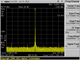
One final test is can you verify if you are able to capture on the ADC without any errors?
Based on the results that you have shared so far it looks like the issue could be with the EVM and if the ADC results above shows a similar issue we can look into ways to replace your EVM with a new one (Most likely through the vendor that it was purchased through).
Regards,
David Chaparro
Hi David,
I captured the data on an ADC. It seems like there are no errors. But the SNR is 20 dB lower than the results shown in Step 8 of your document.
I am attaching screenshots for channels PxA, B, C (D - there is no connector).
An input signal level of 5 dBm is the best option for SNR.
The problem with the parasitic frequency harmonics of the DAC has not gone away. It seems that instead of one NCO there are two NCOs.
Sincerely,
Andrey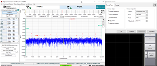
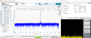
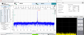
Hi Andrey,
Was this EVM purchased from TI or from a distributor?
Regards,
David
Hi David,
Both EVM modules (595-RF1208AFE7950EVM and 595-TSW14J57EVM) were purchased from Mouser Electronic (www.mouser.co.il) in March this year.
Have you decided that the RF1208AFE7950EVM module is faulty? Or perhaps both modules need to be replaced?
Sincerely,
Andrey
Hi Andrey,
Yes, based on the results you are seeing it looks like the AFE board may be faulty and I would recommend it being replaced through your distributor.
Regards,
David Chaparro