This thread has been locked.

If you have a related question, please click the "Ask a related question" button in the top right corner. The newly created question will be automatically linked to this question.

AFE7950: SYSREF signal functional logic requirement

Part Number: AFE7950
Other Parts Discussed in Thread: LMK04832

Tool/software:

Hi, 

We planned to use AFE7950 Part in our design.

In data sheet , SYSREF Requirements given as below.

Three SYSREF pulses are required to
completely synchronize the device.28. These three pulses are necessary to synchronize the N-divider (if
needed), clock divider for the digital logics, and the JESD204 link-up. SYSREF usage in the bring-up software
flow is described in the AFE79xx Configuration Guide available from TI. For each pulse, a SPI register latch is
programmed high, after which the 1st SYSREF pulse is captured and the following pulses are ignored. SYSREF
then would need to be held low for the SPI latch to be programmed low then high again for the next pulse. After
the 3 pulses, TI recommends that SYSREF is turned off or held low to prevent spurs coupling into the device
clock

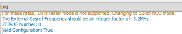
How to calculate the SYS-REF Clock frequency range ? In data sheet mentioned to refer the "Excel spreadsheet to calculate possible SYSREF frequencies is available from TI". Please share teh spreadsheet for reference.

And also what is the relationship between SPI latch to SYS-REF signal ? Why SYS-REF signal is referred with SPI signal?

Please share the detailed functional requirement of SYS-REF signal?

  • Hi Gurusamy,

    As you mentioned the AFE does require sysref pulses during device configuration and there are two methods of doing this. The first is to use a continuous SYSREF during the AFE configuration and the AFE will use three of the SYSREF edges to align everything internally. The second option is the one you describe above, which is to use a pulsed SYSREF and provide the pulses at the exact points of the AFE bringup sequence. In both modes the SYSREF can be disabled after the AFE bringup to prevent spurs coupling into the device clock. 

    For the SYSREF frequency we no longer recommend using the spreadsheet and have removed this from the folder. Instead our recommendation is to load your mode in the AFE79xx GUI and when you run the AFE bringup it will report the max SYSREF frequency in the log window. 

    The SPI latch is used so that we can gate when a SYSREF pulse is used by the AFE. This is helpful to prevent the AFE from using any unexpected glitch/edge on the SYSREF lines to realign the device. 

    Please see the section 7.10 "Timing Requirements" in the datasheet for the SYSREF setup and hold time requirements. 

    Regards,

    David Chaparro 

  • Hi David,

    Thanks for your valuable response.

    As of my understanding that the requirement of SYSREF, during the AFE bringup time only SYSREF signal needed after that it wont be used.

    I am going to interface the 1No of AFE7950 chip with XCKU060 Kintex ultrascale FPGA.

    Generate the device clock of FPGA and AFE Chip by using LMK04832 chip.

    While PCB design, what are the length Matching to be done between the AFE Device clock to SYSREF clock signal and also , Does i need to length Match the FPGA device clock to SYSREF signal of FPGA ?.

    Does length matching need to be done between the SYSREF-REQUEST/Sync signal routed from LMK to FPGA ?

  • Hi Gurusamy,

    The first question is answered on your other post, linked below.

    https://e2e.ti.com/support/rf-microwave-group/rf-microwave/f/rf-microwave-forum/1496622/afe7950-sp-reg---clock-and-sysref-path-in-afe7950/ 

    In regard to the SYSREF request pin/Sync signal, length matching on this would only be needed if you have multiple LMKs and they needed to be aligned/synchronized. If only one LMK is being used then it does not need to be length matched to anything. 

    Regards,

    David Chaparro