This thread has been locked.

If you have a related question, please click the "Ask a related question" button in the top right corner. The newly created question will be automatically linked to this question.

LDC1612:the question of register configuration

Part Number: LDC1612

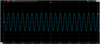
Some questions about LDC1612 register configuration.
I want to use a function like this:
 1. Only use CH0;
 2. Full precision conversion time;
 3. The INTB Pin generates a falling edge interrupt when the conversion is complete;
My register configuration is as follows:

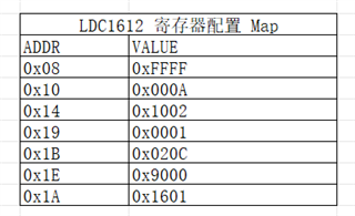
Are there any questions ?

  • Hello Max,

    From the settings you have, I see that you have chosen the longest possible conversion time, and higher conversion time generally leads to higher resolution.  Looks like you are providing an external clock for a more stable oscillator and have overriding Rp set to have consistent current drive for more consistent measurements.  From the config register I see that you have continuous conversion of Channel 0 selected and the error config register has the assertion of INT B enabled.  Therefore, it looks like you have properly configured the registers for the settings you desire.

  • Hello,

    I write the registers value according to the table, and verified by reading the register values.

    But on the INTB pin, the falling edge is not captured.

    My hardware connections are as follows:

    I also disconnected the INTB pin from the MCU, and used an oscilloscope to capture the falling edge, but still nothing.

    What could be the problem?

  • Hey Max,

    It could be related to setup and hold times on your communication lines.  The logic chains for read and write commands for configuration registers might be a little more forgiving with the timing specifications while logic that prompts the device to switch to active mode may not be.

    If your communication lines look like they are meeting all the timing specs, then you might want to probe your external clock or IN0A and IN0B.  A quick continuity test of your IN0A and IN0B lines might help.

  • hello.

      I just replaced the MCU from MSP430 to STM32 and the others are consistent with LDC1612 EVM.

      there is still nothing on the pin of INTB.


      Is there a difference in I2C timing for configuring different registers?


      How can I confirm the problem with IN0A and IN0B?

  • Hello Max,

    So based on prior threads you have programmed the device in the order prescribed in table 47 of the datasheet, then read back those registers to verify that the registers are configured correctly.  The next step would be to check IN0A and IN0B on an oscilloscope.  With a differential probe, you should see a signal like in the figure below if everything is correct. Please verify this and send me a scope shot for confirmation.  If you see a normal sine wave during your probing perhaps it might be worthwhile enabling bits 15 through 11 of ERROR_CONFIG register when programming the device, then you can see if there is some sort of error occurring with the output register. 

    I presume that INTB is stuck high.  However, I would suggest pulling scope out of single trigger mode for a sanity check. If you find INTB is low, you can read the status register to check DRDY and trigger INTB to change for the next complete conversion.

  • Hello Patrick,

      Today,  after I read the DATAx_MSB/DATAx_LSB register, I read the status register (addr 0x18) immediately, and a falling edge signal can appear on INTB. It seems that reading the status register can clear the interrupt event, is that true? To trigger the DATA_READY signal with INTB, do I need to read the status register every time?

  • Hello Max,

    Per the Device Status Registers section of the datasheet, reading the status register is one of the events that clears an interrupt.  Every time the INTB pin asserts, you will need to read the status register to clear the data ready bit.

  • thanks for your answer.