This thread has been locked.

If you have a related question, please click the "Ask a related question" button in the top right corner. The newly created question will be automatically linked to this question.

IWR6843AOP: Uart bootloader uses CH340, a self-designed circuit board

Part Number: IWR6843AOP
Other Parts Discussed in Thread: IWR6843, UNIFLASH, , ALP

Hi everybody,

I'm developing a circuit board using the IWR6843 and I have the following questions.

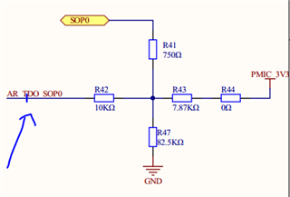
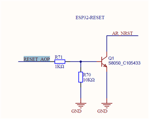
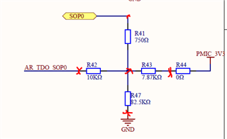
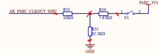
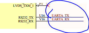
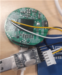
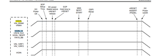
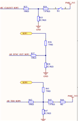
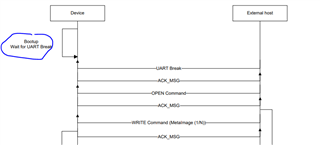
I want to use UNIFLASH to flash IWR6843AOP chip over UARTA using USB TO UART CH340, in my design removed USB TO UART CP2105, below is my uart block design:

In my design, I tested sources from the PMIC generating 3.3V, 1.2V, 1.0V, 1.8V all working fine.

VDDIN = 1.19 v

VION_18 = 1.73 v

VIN_13RF1 = 1.02 v


VIOIN = 3.33v

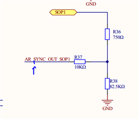
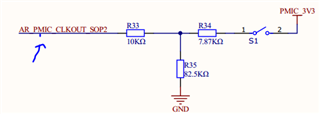
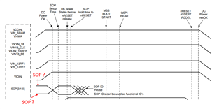
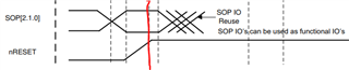
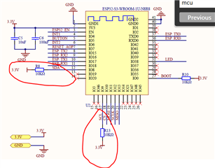
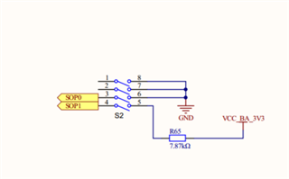
SOP0, SOP1, SOP1 should be placed in the correct position (1 0 1 _ flash_mode):

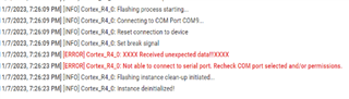
But UNIFLASH started flashing to IWR6843, showing the following error:

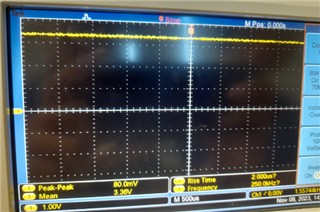
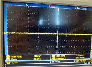
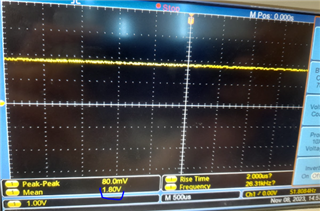
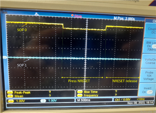
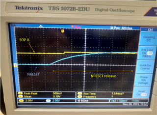
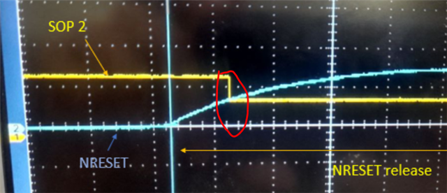
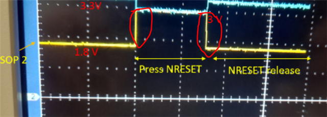
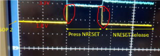
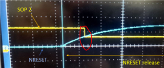
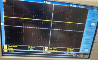
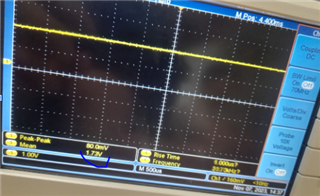
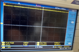
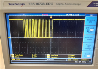
i guess the flashing process via UART is being stopped here, when UNIFLASH sends interrupt signal to IWR6843, it gets no response or wrong response from IWR6843. I used an oscilloscope to measure pulses from the IWR6843AOP circuit board and the circuit board I designed myself, the results are as follows:

  • The pulse I measured is from the UARTA_TX pin of the IWR6843AOP board

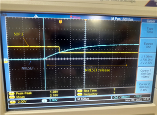
  • The pulse I measured is from the UARTA_TX pin of the circuit board I designed


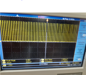
=>The pulse measured from the IWR6843AOP circuit board responding when receiving a break signal from UNIFLASH is different from the pulse measured from the circuit board I designed myself.

I am willing to provide my board design to solve this problem.

I have the following questions:

        1.Can I FLASH my design board over UART using USB TO UART CH340? If not, which USB TO UART should I use to flash my circuit board.

  1. Does the IWR6843 on my board automatically send a signal break to UNIFLASH, or do I have to simulate a signal break somehow to send it to UNIFLASH?

I look forward to receiving your help regarding the problem I have encountered

Thanks and Regards,

Tu Tran


  • Hi Tu Tran,

    1. Any USB TO UART converter should work fine for the flashing the device.

    2. The IWR6843 device should automatically send a signal break to UNIFLASH.

    I suspect the device has not booted up in the correct SOP mode. All the oscilloscope capture are after they are stable, could you please probe the supply lines and SOP signals at the time of reset release. We should ensure that the NRESET release happens only after the power supplies and SOP signals are stable so that it can latch the correct bootmode.

    Regards

    Ankit

  • Thanks for the feedback
    I used an oscilloscope to check pins SOP0, SOP1, SOP2 in flash mode and the results are as follows:

    SOP0 = 3.36v:

    SOP1: 

    SOP2: 1.8V


    Below is the power supply schematic:

    I look forward to receiving your help as soon as possibleGrinning

    Regards

    Tu Tran

  • Hi Tran,

    Please capture the SOP and power signals during NRESET release along with the RESET signal. The above captures are once these signals are stable and won't help in determining if the correct bootmode is latched.

    Regards

    Ankit

  • Thanks for the feedback
    I will check and give the results as soon as possible

    Regards

    Tu Tran

  • I am grateful for the response to my post
    The steps I take are as follows:
    1. Power the board
    2. Press the NRESET button
    3. After a period of time, release NRESET
    My meter can only measure 2 channels at the same time and I have the following results:
    + SOP 0 and SOP2:

    + SOP 0 and SOP2:

    Is the signal I measured correct to select flash mode?
    Can you explain specifically to me where SOP0, SOP1, SOP2 are in this drawing?

    I will check and give the results as soon as possible

    Regards

    Tu Tran

  • Hi,

    It would be helpful if you could capture SOP0 and NRESET signal and SOP2 and NREST signal individually as you can measure only two signals at a time. The NRESET release will be in microseconds, so we should set the timeframe close to 20-40us and trigger the oscilloscope for rising edge of NREST signal probe.

    For the drawing there is no specific SOP2,1,0 it's just a depiction of SOP signals and can be set high or low according to the bootmode selected. The important part is that during the reset release all the SOP signals are stable. 

    Regards

    Ankit

  • I'm so grateful for your response
    I will measure the signal again and post the results tomorrow

    Best regards

    Tu Tran

  • Hi,

    I measured at the two signal ends NRESET, SOP0 and NRESET, SOP2, the results are as follows:

    + NRESET, SOP 0

    + NRESET, SOP 2

    I look forward to receiving your help as soon as possible

    Regards

    Tu Tran

  • Tran,

    Yes, the wrong bootmode is being latched during NRESET release. Hence, you are unable to flash your device. Also, it appears some signal to be driving the signal when reset is released. The SOP2 signal should not drop when reset is released. As during reset release SOP2 is below threshold voltage of 3.3V incorrect SOP mode is set.

    Please provide the schematics, so I may review and let you know.

    Also, it appears that the SOP signals capture shared before seem to different from what is shared now. Could you please confirm.


    Regards

    Ankit

  • Hi,

    I'm very grateful for your feedback
    I will explain more about this photo:

    =>The yellow signal is SOP2, the blue signal is SOP0. I measured these two signals at the same time, the yellow arrow (Press NRESET) and (NRESET release) is the time I pressed the nRESET button and released it on my circuit board.

    In the picture below, I measure 2 signals at the same time: yellow is the SOP2 signal, the other color is the signal at the NRESET pin.

    Do you mean that during NRESET release, the signal at SOP2 must not drop and must be at 3.3v for the device to go into flash modeWink?

    This is my design, please help me check this design:

    https://drive.google.com/file/d/1iiuyPQqyTQGmDOLGFNwpvuX-KqtMEhd3/view?usp=sharing

    I look forward to receiving your help as soon as possible

    Regards

    Tu Tran

  • Tran,

    Thanks for the explanation. But SOP2 must not drop and be 3.3V for the device to go into flash mode.

    I will check the schematic and provide the feedback.

    Regards

    Ankit

  • Hi,
    I am very grateful and look forward to receiving your earliest response

    Regards

    Tu Tran

  • Hi Tran,

    Can you please share the schematic here or in a private conversation. I am not able to access the gdrive.

    Regards

    Ankit

  • Hi, 

    Sorry for the inconvenience, here is my schematic:

    Radar_sensor.pdf

    Regards

    Tu Tran

  • Tran,

    Thanks for the schematic. I have put it in schematic review queue, I will get back with some feedback by next week.

    Regards

    Ankit

  • Hi Ankit,

    I look forward to receiving your earliest supportSmile

    Regards

    Tu Tran

  • Hi Tran,

    I reviewed the schematic, it looks good. Could not find any signal that would be driving SOP2 to 1.8V instead of 3.3V. 

    Also, could you please let me know the purpose of the RESET_AOP. Is it supposed to reset the 6843AOP device from the MCU? Can we depopulate the R71 and check if the SOP lines have the same behaviour.

    Regards

    Ankit

  • Hi,

    I'm very grateful for your feedback
    1. My purpose is to use RESET_AOP to USE the ESP32 chip to trigger iwr6843 reset. But in my design I still haven't soldered the RESET_AOP block onto my circuit board. so I'm sure RESET_AOP doesn't affect the measurement results.
    2. at SOP2 when applying power I always measure 1.8v, I don't understand why. i tried checking my circuit board and sure enough the sop2 generator is not connected to the 1.8v of the PMIC. Is there any reason when creating sop2 I always measure 1.8v instead of 3.3v?
    3. According to your opinion, when sop2 enters flash mode, there is always a voltage of 3.3v, is that correct?

    Regards

    Ankit

  • Hi Tran,

    Please check below. Although the MCU is not soldered same nets of SDA and SCL are pulled up by the 3.3V instead of VCC_IO or PMIC_3V3. Hence its, booting up the device although when VCC_IO is not present. 

    3. Yes, hen sop2 enters flash mode, there is always a voltage of 3.3v.

    The SDA and SCL nets going to the 6843AOP device must be pulled up by PMIC_3V3 and not 3.3V from LDO. Please try depopulating R8 and R13 and tie to PMIC_3V3. 

    Regards

    Ankit

  • Hi Ankit,

    I'm very grateful for your feedback

    1.All the components below I have not soldered to my circuit board,

    Therefore, SCL and SDA should always use PMIC3.3v power:


    .I will send you back my design, in this version I have marked the actual soldered components on my circuit board. Could you please check again, sorry for the inconvenience.

    radar_sensor_edit.pdf
    2.Will not soldering the QSPI_Flash or failing to solder it have any effect on SOP2?

    Regards

    Tu Tran

  • Tran,

    1. Thank you for clarifying.

    2. Yes, not having QSPI will impact the firmware loading if not exactly the SOP2 signal. The IWR6843AOP device loads the firmware bin or appimage file from the serial QSPI flash to RAM. Could you please try soldering QSPI flash and then load the program over UNIFLASH.

    Regards

    Ankit

  • Hi,

    I'm very grateful for your feedback

    "The IWR6843AOP device loads firmware bins or application image files from serial QSPI flash into RAM." I understand this very well. and I just want to check the effect of QSPI_FLASH on the voltage level at SOP2 when NRESET_release

    1. I tried 2 cases: soldering QSPI_FLASH and not soldering QSPI_FLASH, but the voltage at pin SOP2 in both cases is 1.8v when in flash mode. The result is no change, I cannot download the program via UNIFLASH. Can you explain clearly to me how QSPI_FLASH affects the voltage level at SOP2 when NRESET release is in flash mode?
    2. Can you check the design below, I have marked the components to be soldered on my circuit board

    3022.radar_sensor_edit.pdf
    Am I missing something in my design?

    Regards

    Tu Tran

  • Hi,

    This is the iwr6843aop module I am using on my design:

    "WR6843 IQR ALP"

    Regards

    Tu Tran

  • Hi Tran,

    1. Voltage at pin SOP2 is independent of QSPI flash. The serial QSPI_FLASH does not affect the voltage level at SOP2 when NRESET release is in flash mode. If you cannot download the program even after soldering the QSPI flash, seems the issue persists with the SOP2 voltage.

    2. Please allow me some time till early next week to go through the updated schematic again. Please do check that all digital IO pins of the device (except NRESET) are non-failsafe; hence, care needs to be taken that they are not driven externally without the VIO supply being present to the device.

    Regards

    Ankit

  • Hi Tran,

    I went over the schematic; I could not find any signal that could be pulling down the SOP2 signal to 1.8V from 3.3V. Would you kindly assist me in measuring the resistors below and provide their values?

    R41, R44, R47, R42 and the junction.

    R33, R34, R35 and the junction

    Regards

    Ankit

  • Tran,

    It appears that the problem is not with SOP mode registration. Could you kindly verify by connecting to JTAG and reading the SOP mode registers?

    SOP mode register: FFFF E268 (Flash mode should read 0x00000005, Functional Mode should read 0x00000001)

    Also, can you let me know how you are trying to flash the device; I see the AR_MSS_LOGGER been brought out as a test point. Can you please confirm if it is connected to a UART to USB converter to collect and process the output data.

  • Hi Ankit,

    Thanks for the feedback,
    1. can you clearly explain how to test by connecting to JTAG and reading SOP mode registers?
    2. yes, I use AR_MSS_LOGGER as a test point, but I don't use it. It's just a backup plan.
    I use CH340 connected to UARTA_TX and UARTA_RX to load program into QSPI_FLASH.


    3. Can you please check my PCB design.

    I am truly grateful for your supportGrin

    Regards

    Tu tran

  • Hi Tran,

    1. You may be able to read SOP mode registers by connecting to Cortex_M4 core using Code Composer Studio over JTAG. 


    2. Thank you for explaining. Did you try connecting TX pin of device to TX pin of CH340 and same for RX pins and also by connecting TX of device to RX CH340 and vice versa. Sometimes the pin definitions for USB to UART converter are different wrt device.

    3. Sure, I can review the PCB design. Please send it in ODB++ or Altium PCB project format.

    Regards

    Ankit

  • Hi Ankit,

    Thank you for your feedback
    For some reason, I cannot provide my design here Sweat smile

    Can you give me your personal contact address like email..?

    Regards

    Tu tran

  • Hi Tran,

    I have sent you a connection request. Please accept, I may give my mail there.

    Regards

    Ankit