This thread has been locked.

If you have a related question, please click the "Ask a related question" button in the top right corner. The newly created question will be automatically linked to this question.

AWR2944: AWR2944 ES1.0 to ES2.0 the CSi2 mode cannot receive

Part Number: AWR2944
Other Parts Discussed in Thread: SYSCONFIG, UNIFLASH

Hi,

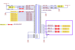
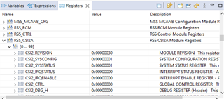
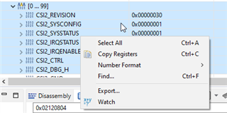
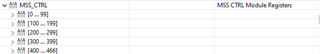
    I debugged the CSI2 mode by running it on the AWR 2844 ES1.0.

    but when zhe AWR2944 ES1.0 to ES2.0 changes,zhe CSI2 mode cannot receive.

    There are no changes related to CSI2 in the modification information from ES1.0 to ES2.0.

   May I ask if there is any good solution?

Regards,

guilin.shi

  • Hello Shi,

    What version of the SDK are you using?  If you are using a much older version of the SDK intended for use with ES1.0, then you should try upgrading to the latest SDK.  Please try that and let us know what you find.   

    https://www.ti.com/tool/MMWAVE-MCUPLUS-SDK

    Best Regards,

    James

  • Hello James,

    The SDK version I am using si mmwave_mcuplus_sdk_04_02_00_03.

    I compared two versions of SDKs and found that their CSI2 module is consistent.

    At that time, debugging was implemented through CSI2 on ES1.0 based on the modification of E2E.(AWR2944: receive data from CSI2 - Sensors forum - Sensors - TI E2E support forums

    I am trying to use the latest SDK version,The CSI2 module is still not working properly.

    Regards,

    guilin.shi

  • Hello James,

    I found the problem in isResetDone by debugging the code.

    The main issue during ES1.0 debugging is the Drivers_csirxInstanceOpen function.

    The following is the code that I debugged successfully in ES1.0 at that time.

    ===========================

    int32_t Drivers_csirxInstanceOpen(uint32_t instanceId, uint16_t numContexts, CSIRX_ContextConfig *pContextConfig)
    {
    int32_t status = SystemP_SUCCESS;

    gCsirxHandle[instanceId] = CSIRX_open(CONFIG_CSIRX0);
    if(gCsirxHandle[instanceId] == NULL)
    {
    status = SystemP_FAILURE;
    DebugP_logError("CSIRX %d: CSIRX_open failed !!!\r\n", instanceId);
    }
    if(status==SystemP_SUCCESS)
    {
    status = CSIRX_reset(gCsirxHandle[instanceId]);
    if(status!=SystemP_SUCCESS)
    {
    DebugP_logError("CSIRX %d: CSIRX_reset failed !!!\r\n", instanceId);
    }
    }
    if(status==SystemP_SUCCESS && gCsirxPhyEnable[instanceId])
    {
    status = CSIRX_complexioSetConfig(gCsirxHandle[instanceId], &gCsirxComplexioConfig[instanceId]);
    if(status!=SystemP_SUCCESS)
    {
    DebugP_logError("CSIRX %d: CSIRX_complexioSetConfig failed !!!\r\n", instanceId);
    }

    if(status==SystemP_SUCCESS)
    {
    status = CSIRX_complexioDeassertReset(gCsirxHandle[instanceId]);
    if(status!=SystemP_SUCCESS)
    {
    DebugP_logError("CSIRX %d: CSIRX_complexioDeassertReset failed !!!\r\n", instanceId);
    }
    }

    if(status==SystemP_SUCCESS)
    {
    status = CSIRX_dphySetConfig(gCsirxHandle[instanceId], &gCsirxDphyConfig[instanceId]);
    if(status!=SystemP_SUCCESS)
    {
    DebugP_logError("CSIRX %d: CSIRX_dphySetConfig failed !!!\r\n", instanceId);
    }
    }
    }
    if(status==SystemP_SUCCESS)
    {
    status = CSIRX_commonSetConfig(gCsirxHandle[instanceId], &gCsirxCommonConfig[instanceId]);
    if(status!=SystemP_SUCCESS)
    {
    DebugP_logError("CSIRX %d: CSIRX_commonSetConfig failed !!!\r\n", instanceId);
    }
    }
    if(status==SystemP_SUCCESS && gCsirxPhyEnable[instanceId])
    {
    status = CSIRX_complexioAssertForceRxModeOn(gCsirxHandle[instanceId]);
    if(status!=SystemP_SUCCESS)
    {
    DebugP_logError("CSIRX %d: CSIRX_complexioAssertForceRxModeOn failed !!!\r\n", instanceId);
    }

    if(status==SystemP_SUCCESS)
    {
    uint32_t numForceRxModeDeassertedPolls = 0;
    bool isForceRxModeDeasserted = false;

    /* wait until force rx mode deasserted: This may depend on Tx */
    do
    {
    status = CSIRX_complexioIsDeassertForceRxModeOn(gCsirxHandle[instanceId],
    &isForceRxModeDeasserted);
    if(status != SystemP_SUCCESS)
    {
    break;
    }
    ClockP_usleep(1000);
    numForceRxModeDeassertedPolls++;
    } while( (isForceRxModeDeasserted == false) && (numForceRxModeDeassertedPolls < 5) );

    if(isForceRxModeDeasserted == false)
    {
    status = SystemP_SUCCESS;
    }
    if(status!=SystemP_SUCCESS)
    {
    DebugP_logError("CSIRX %d: CSIRX_complexioIsDeassertForceRxModeOn failed !!!\r\n", instanceId);
    }
    }
    }
    if(status==SystemP_SUCCESS)
    {
    /* enable interface */
    status = CSIRX_commonEnable(gCsirxHandle[instanceId]);
    if(status!=SystemP_SUCCESS)
    {
    DebugP_logError("CSIRX %d: CSIRX_commonEnable failed !!!\r\n", instanceId);
    }
    }
    if(status==SystemP_SUCCESS && gCsirxPhyEnable[instanceId])
    {
    /* Power on complex IO */
    status = CSIRX_complexioPowerOn(gCsirxHandle[instanceId]);
    if(status!=SystemP_SUCCESS)
    {
    DebugP_logError("CSIRX %d: CSIRX_complexioPowerOn failed !!!\r\n", instanceId);
    }

    if(status == SystemP_SUCCESS)
    {
    uint32_t numComplexioPowerStatusPolls = 0;
    uint8_t powerStatus = 0;

    /* Wait until complex IO powered up */
    numComplexioPowerStatusPolls = 0;

    if(status!=SystemP_SUCCESS)
    {
    DebugP_logError("CSIRX %d: CSIRX_complexioGetPowerStatus failed !!!\r\n", instanceId);
    }
    }
    }
    if(status==SystemP_SUCCESS)
    {
    uint32_t i;

    for(i = 0; i < numContexts; i++)
    {
    /* config contexts */
    status = CSIRX_contextSetConfig(gCsirxHandle[instanceId], i, &pContextConfig[i] );
    if(status!=SystemP_SUCCESS)
    {
    DebugP_logError("CSIRX %d: CSIRX_contextSetConfig for context %d failed !!!\r\n", instanceId, i);
    }
    if(status != SystemP_SUCCESS)
    {
    break;
    }
    }
    }
    if(status==SystemP_SUCCESS)
    {
    /* Debug mode, first flush FIFO - disable debug mode and enable interface */
    status = CSIRX_debugModeDisable(gCsirxHandle[instanceId]);
    if(status!=SystemP_SUCCESS)
    {
    DebugP_logError("CSIRX %d: CSIRX_debugModeDisable failed !!!\r\n", instanceId);
    }
    }
    if(status==SystemP_SUCCESS)
    {
    /* enable interface */
    status = CSIRX_commonEnable(gCsirxHandle[instanceId]);
    if(status!=SystemP_SUCCESS)
    {
    DebugP_logError("CSIRX %d: CSIRX_commonEnable failed !!!\r\n", instanceId);
    }
    }
    CSIRX_contextEnable(gCsirxHandle[instanceId], 0);
    CSIRX_contextEnable(gCsirxHandle[instanceId], 1);

    if(status==SystemP_SUCCESS && gCsirxPhyEnable[instanceId])
    {
    bool isResetDone = false;
    uint8_t powerStatus = 0;
    int count = 0;
    /* Wait until complex IO reset complete */
    do
    {
    CSIRX_complexioGetPowerStatus(gCsirxHandle[instanceId], &powerStatus);
    if (powerStatus == CSIRX_COMPLEXIO_POWER_STATUS_ON)
    {
    GPIO_pinWriteHigh(LICH_BASE_ADDR, LICH_PIN);
    status = CSIRX_complexioIsResetDone(gCsirxHandle[instanceId], &isResetDone);
    if(status!=SystemP_SUCCESS)
    {
    break;
    }
    }
    ClockP_usleep(10);
    ++count;

    } while(isResetDone == false && count < 5400);

    if(isResetDone == false)
    {
    status = SystemP_FAILURE;
    }
    if(status!=SystemP_SUCCESS)
    {
    DebugP_logError("CSIRX %d: CSIRX_complexioIsResetDone failed !!!\r\n", instanceId);
    }
    }
    return status;
    }

    ===========================

    The key issue on ES2.0 is isResetDone != false

    Regards,

    guilin.shi

  • Hello Shi,

    Good find and good work!  However, may I ask if you are planning to update to production devices?

    Best Regards,

    James

  • Hello James,

    I need to ask the relevant personnel tomorrow to answer this question.

    Regards,

    guilin.shi

  • Hello James,

    Does the production devices have an impact on this issue?

    Regards,

    guilin.sh

  • Hi Shi,

    not necessarily, but since it is already RTMed it would probably be a good idea to continue development on the production device.

    Regards,

    James

  • Hello James,

    I am planning to update to production devices.

    The current issue is that it arises in prodction devices.

    This problem arises when I am update AWR2944 ES1.0 to ES2.0 on my production devices.(No changes were made to the other circuits, only the main chip was updated)

    Regards,

    guilin.shi

  • Hello James,

    Is there any update on this issue? Looking forward to your reply.

    Regards,

    guilin.shi

  • Hello shi,

    You have again placed a count for isResetdone, can you remove it and see how long it takes to receive the signal?
    If your FPGA works with ES 1.0 then it should be functional with ES 2.0, as there has been no change in CSI2.

    CSIRX_complexioIsResetDone fails only if the pins are not getting the transmitted signals. Have you tried with a different EVM or chip?
    Are you using the EVM, or your custom board? If it is the EVM, to enable CSI2 there are hardware modifications that need to be done:

    By default, there is no CSI2 connection on the EVM you will have to populate those as it is not connected.

    Can you check your hardware properly and the EVM as well. As far as I am aware there is nothing changed with the CSI2 IP from ES 1.0 to ES 2.0.

    Regards,
    Saswat Kumar

  • Hello Saswat,

    I I tried not to use count for isResetdone.The code is as follows,The program cannot exit while.

    ======

    while(isResetDone == false);

    ======

    I used my custom board,This problem arises when I am update AWR2944 ES1.0 to ES2.0 on my custom board.(just update AWR2944)

    Because there are no changes in the manual(AWR294x ES1.0 to ES2.0Migration Guide), I am curious why CSI2 cannot receive messages.

    thanks!

    guilin.shi

  • Hello Shi guilin,

    And have you seen this across multiple samples or a single sample?
    Also any clock changes you have done while migrating?

    Regards,
    Saswat Kumar

  • Hello Saswat,

    This issue was seen on all samples.(update to AWR2944 ES2.0)

    I haven't changed the clock, I just upgraded the SDK.

    Our hardware circuits and software have not been changed. ES2.0 software can run on ES1.0 hardware. I am currently using the same program when debugging.

    Regards,

    guilin.shi

  • Hello Shi guillin,

    Also, can you set a breakpoint after the pass condition in your code, and then take a register dump of CSI2 registers vs the ES 1.0 and the ES 2.0 case?

    Regards,
    Saswat Kumar

  • Hello Saswat,

    I dump of CSI2 registers vs the ES 1.0 and the ES 2.0.

    How can I send you the file? There is no attachment file included in this file.

    Can you give me your email so that I can send you the files via email.

    Regards,

    guilin.shi

  • Hello Shi guillin,

    For the registers that are different can you send me ss, or CCS also has the capacity to copy the registers into plain text which can be copied to .txt which you can upload directly on e2e.

    Regards,
    Saswat Kuamr

  • Hello Saswat,

    The following is the dump value of the CSI2 register.

    ES1.0

    ========

      Offset: 00 01 02 03 04 05 06 07 08 09 0A 0B 0C 0D 0E 0F
    00000000: 30 00 00 00 00 00 00 00 00 00 00 00 00 00 00 00 0...............
    00000010: 01 20 00 00 01 00 00 00 00 00 00 00 03 00 00 00 ................
    00000020: 00 00 00 00 00 00 00 00 00 00 00 00 00 00 00 00 ................
    00000030: 00 00 00 00 00 00 00 00 00 00 00 00 00 00 00 00 ................
    00000040: 79 20 00 00 00 00 00 00 1B 00 00 00 00 00 00 20 y...............
    00000050: 13 02 00 6A 00 00 00 00 00 00 00 00 00 00 00 00 ...j............
    00000060: E7 9C 73 00 00 00 00 00 00 00 00 00 FF 7F FF 7F g.s.............
    00000070: 03 00 01 00 2A 00 00 00 00 00 00 00 00 50 23 88 ....*........P#.
    00000080: 00 50 23 88 8F 00 00 00 00 00 00 00 01 00 00 00 .P#.............
    00000090: 0B 00 01 00 2A 08 00 00 00 00 00 00 00 00 00 A4 ....*..........$
    000000a0: 00 00 00 A4 8F 00 00 00 00 00 00 00 01 00 00 00 ...$............
    000000b0: 08 00 01 00 00 00 00 00 00 00 00 00 00 00 00 00 ................
    000000c0: 00 00 00 00 00 00 00 00 00 00 00 00 00 00 00 00 ................
    000000d0: 08 00 01 00 00 00 00 00 00 00 00 00 00 00 00 00 ................
    000000e0: 00 00 00 00 00 00 00 00 00 00 00 00 00 00 00 00 ................
    000000f0: 08 00 01 00 00 00 00 00 00 00 00 00 00 00 00 00 ................
    00000100: 00 00 00 00 00 00 00 00 00 00 00 00 00 00 00 00 ................
    00000110: 08 00 01 00 00 00 00 00 00 00 00 00 00 00 00 00 ................
    00000120: 00 00 00 00 00 00 00 00 00 00 00 00 00 00 00 00 ................
    00000130: 08 00 01 00 00 00 00 00 00 00 00 00 00 00 00 00 ................
    00000140: 00 00 00 00 00 00 00 00 00 00 00 00 00 00 00 00 ................
    00000150: 08 00 01 00 00 00 00 00 00 00 00 00 00 00 00 00 ................
    00000160: 00 00 00 00 00 00 00 00 00 00 00 00 00 00 00 00 ................
    00000170: 27 04 00 01 0E E1 02 F0 FF 00 00 00 A0 C0 41 10 '....a.p.....@A.
    00000180: 00 00 00 00 84 21 01 00 0C 20 0D 00 00 00 00 00

    ========

    ES2.0

    =======

    Offset: 00 01 02 03 04 05 06 07 08 09 0A 0B 0C 0D 0E 0F
    00000000: 30 00 00 00 00 00 00 00 00 00 00 00 00 00 00 00 0...............
    00000010: 01 20 00 00 01 00 00 00 00 00 00 00 03 00 00 00 ................
    00000020: 00 00 00 00 00 00 00 00 00 00 00 00 00 00 00 00 ................
    00000030: 00 00 00 00 00 00 00 00 00 00 00 00 00 00 00 00 ................
    00000040: 79 20 00 00 00 00 00 00 1B 00 00 00 00 00 00 00 y...............
    00000050: 13 02 00 4A 00 00 00 00 00 00 00 00 00 00 00 00 ...J............
    00000060: E7 9C 73 00 00 00 00 00 00 00 00 00 FF FF FF 7F g.s.............
    00000070: 0B 00 01 00 2A 00 00 00 00 00 00 00 00 50 23 88 ....*........P#.
    00000080: 00 50 23 88 8F 00 00 00 00 00 00 00 01 00 00 00 .P#.............
    00000090: 0B 00 01 00 2A 08 00 00 00 00 00 00 00 00 00 A4 ....*..........$
    000000a0: 00 00 00 A4 8F 00 00 00 00 00 00 00 01 00 00 00 ...$............
    000000b0: 08 00 01 00 00 00 00 00 00 00 00 00 00 00 00 00 ................
    000000c0: 00 00 00 00 00 00 00 00 00 00 00 00 00 00 00 00 ................
    000000d0: 08 00 01 00 00 00 00 00 00 00 00 00 00 00 00 00 ................
    000000e0: 00 00 00 00 00 00 00 00 00 00 00 00 00 00 00 00 ................
    000000f0: 08 00 01 00 00 00 00 00 00 00 00 00 00 00 00 00 ................
    00000100: 00 00 00 00 00 00 00 00 00 00 00 00 00 00 00 00 ................
    00000110: 08 00 01 00 00 00 00 00 00 00 00 00 00 00 00 00 ................
    00000120: 00 00 00 00 00 00 00 00 00 00 00 00 00 00 00 00 ................
    00000130: 08 00 01 00 00 00 00 00 00 00 00 00 00 00 00 00 ................
    00000140: 00 00 00 00 00 00 00 00 00 00 00 00 00 00 00 00 ................
    00000150: 08 00 01 00 00 00 00 00 00 00 00 00 00 00 00 00 ................
    00000160: 00 00 00 00 00 00 00 00 00 00 00 00 00 00 00 00 ................
    00000170: 27 04 00 01 0E E1 02 C0 FF 00 00 00 A0 C0 01 00 '....a.@.....@..
    00000180: B4 D6 5A 6B 84 80 00 00 0E 20 0D 00 00 00 00 00

    =======

    Regards,

    guilin.shi

  • Hello Shi,

    I had requested for the register values that is present in the CCS in the top right corner under the registers tab itself:

    You can copy registers as well in notepad:

    In both failing and passing case share me the CSI2, MSS_TOPRCM, MSS_RCM and MSS_CTRL
    Direct dump like that it very hard to decode and time consuming as well, I would appreciate if you can give in a format like the registers I have attached below:

    RSS_CSI2A		RSS CSI2A Module Registers	
    	[0 ... 99]			
    		CSI2_REVISION	0x00000030	MODULE REVISION   This register contains the IP revision code in binary coded   digital. For example we have: 0x01 = revision 0.1 and 0x21   = revision 2.1    [Memory Mapped]	
    		CSI2_SYSCONFIG	0x00000001	SYSTEM CONFIGURATION REGISTER   This register is the OCP-socket system configuration   register.    [Memory Mapped]	
    		CSI2_SYSSTATUS	0x00000001	SYSTEM STATUS REGISTER   This register provides status information about the module   excluding the interrupt status register.    [Memory Mapped]	
    		CSI2_IRQSTATUS	0x00000000	INTERRUPT STATUS REGISTER - All contexts   This register associates one bit for each context in order   to determine which context has generated the interrupt. The   context shall be enabled for events to be generated on that   context.   If the  [Memory Mapped]	
    		CSI2_IRQENABLE	0x00000000	INTERRUPT ENABLE REGISTER - All contexts   This register associates one bit for each context in order   to enable/disable each context individually.    [Memory Mapped]	
    		CSI2_CTRL	0x00000000	GLOBAL CONTROL REGISTER   This register controls the CSI2 RECEIVER module. This   register shall not be modified dynamically (except IF_EN bit   field).    [Memory Mapped]	
    		CSI2_DBG_H	0x00000000	DEBUG REGISTER (Header)   This register provides a way to debug the CSI2 RECEIVER   module with no image sensor connected to the module. The   debug mode is enabled by CSI2_CTRL.DBG_EN. Only full 32-bit   values shall be written. The register is  [Memory Mapped]	
    		CSI2_GNQ	0x0000001B	GENERIC PARAMETER REGISTER   This register provide a way to read the generic parameters   used in the design.    [Memory Mapped]	
    		CSI2_COMPLEXIO_CFG2	0x00000000	COMPLEX IO CONFIGURATION REGISTER for the complex IO #2   This register contains the lane configuration for the order   and position of the lanes (clock and data) and the polarity   order for the control of the PHY differential signals in   addit [Memory Mapped]	
    		CSI2_COMPLEXIO_CFG1	0x00000000	COMPLEXIO CONFIGURATION REGISTER for the complex IO #1   This register contains the lane configuration for the order   and position of the lanes (clock and data) and the polarity   order for the control of the PHY differential signals in   additi [Memory Mapped]	
    		CSI2_COMPLEXIO1_IRQSTATUS	0x00000000	INTERRUPT STATUS REGISTER - All errors from complex IO #1    [Memory Mapped]	
    		CSI2_COMPLEXIO2_IRQSTATUS	0x00000000	INTERRUPT STATUS REGISTER - All errors from complex IO #2    [Memory Mapped]	
    		CSI2_SHORT_PACKET	0x00000000	SHORT PACKET INFORMATION -   This register sets the 24-bit DATA_ID + Short Packet Data   Field when the data type is between 0x8 and x0F    [Memory Mapped]	
    		CSI2_COMPLEXIO1_IRQENABLE	0x00000000	INTERRUPT ENABLE REGISTER - All errors from complex IO #1    [Memory Mapped]	
    		CSI2_COMPLEXIO2_IRQENABLE	0x00000000	INTERRUPT ENABLE REGISTER - All errors from complex IO #2    [Memory Mapped]	
    		CSI2_DBG_P	0x00000000	DEBUG REGISTER (Payload)   This register provides a way to debug the CSI2 RECEIVER   module with no image sensor connected to the module. The   debug mode is enabled by CSI2_CTRL.DBG_EN. Only full 32-bit   values shall be written. The register is [Memory Mapped]	
    		CSI2_TIMING	0x7FFF7FFF	TIMING REGISTER   This register controls the CSI2 RECEIVER module. This   register shall not be modified while CSI2_CTRL.IF_EN is set   to '1'.   It is used to indicate the number of L3 cycles for the Stop   State monitoring.    [Memory Mapped]	
    		CSI2_CTX0_CTRL1	0x00010008	CONTROL REGISTER - Context   This register controls the Context. This register is   shadowed: modifications are taken into account after the   next FSC sync code.    [Memory Mapped]	
    		CSI2_CTX0_CTRL2	0x00000000	CONTROL REGISTER - Context   This register controls the Context. This register is   shadowed: modifications are taken into account after the   next FSC sync code (except for VIRTUAL_ID and FORMAT   fields). The change of VIRTUIAL_ID and FORMAT ha [Memory Mapped]	
    		CSI2_CTX0_DAT_OFST	0x00000000	DATA MEM ADDRESS OFFSET REGISTER - Context   This register sets the offset which is applied on the   destination address after each line is written to memory.   This register applies for both CSI2_CTX_DAT_PING_ADDR and   CSI2_CTX_DAT_PONG_ADDR.   [Memory Mapped]	
    		CSI2_CTX0_DAT_PING_ADDR	0x00000000	DATA MEM PING ADDRESS REGISTER - Context   This register sets the 32-bit memory address where the pixel   data are stored. The destination is double buffered: this   register sets the PING address. Double buffering is enabled   when the addresses [Memory Mapped]	
    		CSI2_CTX0_DAT_PONG_ADDR	0x00000000	DATA MEM PONG ADDRESS REGISTER - Context   This register sets the 32-bit memory address where the pixel   data are stored. The destination is double buffered: this   register sets the PONG address. Double buffering is enabled   when the addresses [Memory Mapped]	
    		CSI2_CTX0_IRQENABLE	0x00000000	INTERRUPT ENABLE REGISTER - Context   This register regroups all the events related to Context.    [Memory Mapped]	
    		CSI2_CTX0_IRQSTATUS	0x00000000	INTERRUPT STATUS REGISTER - Context   This register regroups all the events related to Context.    [Memory Mapped]	
    		CSI2_CTX0_CTRL3	0x00000000	CONTROL REGISTER - Context   This register controls the Context. This register is   shadowed: modifications are taken into account after the   next FSC sync code.    [Memory Mapped]	
    		CSI2_CTX1_CTRL1	0x00010008	CONTROL REGISTER - Context   This register controls the Context. This register is   shadowed: modifications are taken into account after the   next FSC sync code.    [Memory Mapped]	
    		CSI2_CTX1_CTRL2	0x00000000	CONTROL REGISTER - Context   This register controls the Context. This register is   shadowed: modifications are taken into account after the   next FSC sync code (except for VIRTUAL_ID and FORMAT   fields). The change of VIRTUIAL_ID and FORMAT ha [Memory Mapped]	
    		CSI2_CTX1_DAT_OFST	0x00000000	DATA MEM ADDRESS OFFSET REGISTER - Context   This register sets the offset which is applied on the   destination address after each line is written to memory.   This register applies for both CSI2_CTX_DAT_PING_ADDR and   CSI2_CTX_DAT_PONG_ADDR.   [Memory Mapped]	
    		CSI2_CTX1_DAT_PING_ADDR	0x00000000	DATA MEM PING ADDRESS REGISTER - Context   This register sets the 32-bit memory address where the pixel   data are stored. The destination is double buffered: this   register sets the PING address. Double buffering is enabled   when the addresses [Memory Mapped]	
    		CSI2_CTX1_DAT_PONG_ADDR	0x00000000	DATA MEM PONG ADDRESS REGISTER - Context   This register sets the 32-bit memory address where the pixel   data are stored. The destination is double buffered: this   register sets the PONG address. Double buffering is enabled   when the addresses [Memory Mapped]	
    		CSI2_CTX1_IRQENABLE	0x00000000	INTERRUPT ENABLE REGISTER - Context   This register regroups all the events related to Context.    [Memory Mapped]	
    		CSI2_CTX1_IRQSTATUS	0x00000000	INTERRUPT STATUS REGISTER - Context   This register regroups all the events related to Context.    [Memory Mapped]	
    		CSI2_CTX1_CTRL3	0x00000000	CONTROL REGISTER - Context   This register controls the Context. This register is   shadowed: modifications are taken into account after the   next FSC sync code.    [Memory Mapped]	
    		CSI2_CTX2_CTRL1	0x00010008	CONTROL REGISTER - Context   This register controls the Context. This register is   shadowed: modifications are taken into account after the   next FSC sync code.    [Memory Mapped]	
    		CSI2_CTX2_CTRL2	0x00000000	CONTROL REGISTER - Context   This register controls the Context. This register is   shadowed: modifications are taken into account after the   next FSC sync code (except for VIRTUAL_ID and FORMAT   fields). The change of VIRTUIAL_ID and FORMAT ha [Memory Mapped]	
    		CSI2_CTX2_DAT_OFST	0x00000000	DATA MEM ADDRESS OFFSET REGISTER - Context   This register sets the offset which is applied on the   destination address after each line is written to memory.   This register applies for both CSI2_CTX_DAT_PING_ADDR and   CSI2_CTX_DAT_PONG_ADDR.   [Memory Mapped]	
    		CSI2_CTX2_DAT_PING_ADDR	0x00000000	DATA MEM PING ADDRESS REGISTER - Context   This register sets the 32-bit memory address where the pixel   data are stored. The destination is double buffered: this   register sets the PING address. Double buffering is enabled   when the addresses [Memory Mapped]	
    		CSI2_CTX2_DAT_PONG_ADDR	0x00000000	DATA MEM PONG ADDRESS REGISTER - Context   This register sets the 32-bit memory address where the pixel   data are stored. The destination is double buffered: this   register sets the PONG address. Double buffering is enabled   when the addresses [Memory Mapped]	
    		CSI2_CTX2_IRQENABLE	0x00000000	INTERRUPT ENABLE REGISTER - Context   This register regroups all the events related to Context.    [Memory Mapped]	
    		CSI2_CTX2_IRQSTATUS	0x00000000	INTERRUPT STATUS REGISTER - Context   This register regroups all the events related to Context.    [Memory Mapped]	
    		CSI2_CTX2_CTRL3	0x00000000	CONTROL REGISTER - Context   This register controls the Context. This register is   shadowed: modifications are taken into account after the   next FSC sync code.    [Memory Mapped]	
    		CSI2_CTX3_CTRL1	0x00010008	CONTROL REGISTER - Context   This register controls the Context. This register is   shadowed: modifications are taken into account after the   next FSC sync code.    [Memory Mapped]	
    		CSI2_CTX3_CTRL2	0x00000000	CONTROL REGISTER - Context   This register controls the Context. This register is   shadowed: modifications are taken into account after the   next FSC sync code (except for VIRTUAL_ID and FORMAT   fields). The change of VIRTUIAL_ID and FORMAT ha [Memory Mapped]	
    		CSI2_CTX3_DAT_OFST	0x00000000	DATA MEM ADDRESS OFFSET REGISTER - Context   This register sets the offset which is applied on the   destination address after each line is written to memory.   This register applies for both CSI2_CTX_DAT_PING_ADDR and   CSI2_CTX_DAT_PONG_ADDR.   [Memory Mapped]	
    		CSI2_CTX3_DAT_PING_ADDR	0x00000000	DATA MEM PING ADDRESS REGISTER - Context   This register sets the 32-bit memory address where the pixel   data are stored. The destination is double buffered: this   register sets the PING address. Double buffering is enabled   when the addresses [Memory Mapped]	
    		CSI2_CTX3_DAT_PONG_ADDR	0x00000000	DATA MEM PONG ADDRESS REGISTER - Context   This register sets the 32-bit memory address where the pixel   data are stored. The destination is double buffered: this   register sets the PONG address. Double buffering is enabled   when the addresses [Memory Mapped]	
    		CSI2_CTX3_IRQENABLE	0x00000000	INTERRUPT ENABLE REGISTER - Context   This register regroups all the events related to Context.    [Memory Mapped]	
    		CSI2_CTX3_IRQSTATUS	0x00000000	INTERRUPT STATUS REGISTER - Context   This register regroups all the events related to Context.    [Memory Mapped]	
    		CSI2_CTX3_CTRL3	0x00000000	CONTROL REGISTER - Context   This register controls the Context. This register is   shadowed: modifications are taken into account after the   next FSC sync code.    [Memory Mapped]	
    		CSI2_CTX4_CTRL1	0x00010008	CONTROL REGISTER - Context   This register controls the Context. This register is   shadowed: modifications are taken into account after the   next FSC sync code.    [Memory Mapped]	
    		CSI2_CTX4_CTRL2	0x00000000	CONTROL REGISTER - Context   This register controls the Context. This register is   shadowed: modifications are taken into account after the   next FSC sync code (except for VIRTUAL_ID and FORMAT   fields). The change of VIRTUIAL_ID and FORMAT ha [Memory Mapped]	
    		CSI2_CTX4_DAT_OFST	0x00000000	DATA MEM ADDRESS OFFSET REGISTER - Context   This register sets the offset which is applied on the   destination address after each line is written to memory.   This register applies for both CSI2_CTX_DAT_PING_ADDR and   CSI2_CTX_DAT_PONG_ADDR.   [Memory Mapped]	
    		CSI2_CTX4_DAT_PING_ADDR	0x00000000	DATA MEM PING ADDRESS REGISTER - Context   This register sets the 32-bit memory address where the pixel   data are stored. The destination is double buffered: this   register sets the PING address. Double buffering is enabled   when the addresses [Memory Mapped]	
    		CSI2_CTX4_DAT_PONG_ADDR	0x00000000	DATA MEM PONG ADDRESS REGISTER - Context   This register sets the 32-bit memory address where the pixel   data are stored. The destination is double buffered: this   register sets the PONG address. Double buffering is enabled   when the addresses [Memory Mapped]	
    		CSI2_CTX4_IRQENABLE	0x00000000	INTERRUPT ENABLE REGISTER - Context   This register regroups all the events related to Context.    [Memory Mapped]	
    		CSI2_CTX4_IRQSTATUS	0x00000000	INTERRUPT STATUS REGISTER - Context   This register regroups all the events related to Context.    [Memory Mapped]	
    		CSI2_CTX4_CTRL3	0x00000000	CONTROL REGISTER - Context   This register controls the Context. This register is   shadowed: modifications are taken into account after the   next FSC sync code.    [Memory Mapped]	
    		CSI2_CTX5_CTRL1	0x00010008	CONTROL REGISTER - Context   This register controls the Context. This register is   shadowed: modifications are taken into account after the   next FSC sync code.    [Memory Mapped]	
    		CSI2_CTX5_CTRL2	0x00000000	CONTROL REGISTER - Context   This register controls the Context. This register is   shadowed: modifications are taken into account after the   next FSC sync code (except for VIRTUAL_ID and FORMAT   fields). The change of VIRTUIAL_ID and FORMAT ha [Memory Mapped]	
    		CSI2_CTX5_DAT_OFST	0x00000000	DATA MEM ADDRESS OFFSET REGISTER - Context   This register sets the offset which is applied on the   destination address after each line is written to memory.   This register applies for both CSI2_CTX_DAT_PING_ADDR and   CSI2_CTX_DAT_PONG_ADDR.   [Memory Mapped]	
    		CSI2_CTX5_DAT_PING_ADDR	0x00000000	DATA MEM PING ADDRESS REGISTER - Context   This register sets the 32-bit memory address where the pixel   data are stored. The destination is double buffered: this   register sets the PING address. Double buffering is enabled   when the addresses [Memory Mapped]	
    		CSI2_CTX5_DAT_PONG_ADDR	0x00000000	DATA MEM PONG ADDRESS REGISTER - Context   This register sets the 32-bit memory address where the pixel   data are stored. The destination is double buffered: this   register sets the PONG address. Double buffering is enabled   when the addresses [Memory Mapped]	
    		CSI2_CTX5_IRQENABLE	0x00000000	INTERRUPT ENABLE REGISTER - Context   This register regroups all the events related to Context.    [Memory Mapped]	
    		CSI2_CTX5_IRQSTATUS	0x00000000	INTERRUPT STATUS REGISTER - Context   This register regroups all the events related to Context.    [Memory Mapped]	
    		CSI2_CTX5_CTRL3	0x00000000	CONTROL REGISTER - Context   This register controls the Context. This register is   shadowed: modifications are taken into account after the   next FSC sync code.    [Memory Mapped]	
    		CSI2_CTX6_CTRL1	0x00010008	CONTROL REGISTER - Context   This register controls the Context. This register is   shadowed: modifications are taken into account after the   next FSC sync code.    [Memory Mapped]	
    		CSI2_CTX6_CTRL2	0x00000000	CONTROL REGISTER - Context   This register controls the Context. This register is   shadowed: modifications are taken into account after the   next FSC sync code (except for VIRTUAL_ID and FORMAT   fields). The change of VIRTUIAL_ID and FORMAT ha [Memory Mapped]	
    		CSI2_CTX6_DAT_OFST	0x00000000	DATA MEM ADDRESS OFFSET REGISTER - Context   This register sets the offset which is applied on the   destination address after each line is written to memory.   This register applies for both CSI2_CTX_DAT_PING_ADDR and   CSI2_CTX_DAT_PONG_ADDR.   [Memory Mapped]	
    		CSI2_CTX6_DAT_PING_ADDR	0x00000000	DATA MEM PING ADDRESS REGISTER - Context   This register sets the 32-bit memory address where the pixel   data are stored. The destination is double buffered: this   register sets the PING address. Double buffering is enabled   when the addresses [Memory Mapped]	
    		CSI2_CTX6_DAT_PONG_ADDR	0x00000000	DATA MEM PONG ADDRESS REGISTER - Context   This register sets the 32-bit memory address where the pixel   data are stored. The destination is double buffered: this   register sets the PONG address. Double buffering is enabled   when the addresses [Memory Mapped]	
    		CSI2_CTX6_IRQENABLE	0x00000000	INTERRUPT ENABLE REGISTER - Context   This register regroups all the events related to Context.    [Memory Mapped]	
    		CSI2_CTX6_IRQSTATUS	0x00000000	INTERRUPT STATUS REGISTER - Context   This register regroups all the events related to Context.    [Memory Mapped]	
    		CSI2_CTX6_CTRL3	0x00000000	CONTROL REGISTER - Context   This register controls the Context. This register is   shadowed: modifications are taken into account after the   next FSC sync code.    [Memory Mapped]	
    		CSI2_CTX7_CTRL1	0x00010008	CONTROL REGISTER - Context   This register controls the Context. This register is   shadowed: modifications are taken into account after the   next FSC sync code.    [Memory Mapped]	
    		CSI2_CTX7_CTRL2	0x00000000	CONTROL REGISTER - Context   This register controls the Context. This register is   shadowed: modifications are taken into account after the   next FSC sync code (except for VIRTUAL_ID and FORMAT   fields). The change of VIRTUIAL_ID and FORMAT ha [Memory Mapped]	
    		CSI2_CTX7_DAT_OFST	0x00000000	DATA MEM ADDRESS OFFSET REGISTER - Context   This register sets the offset which is applied on the   destination address after each line is written to memory.   This register applies for both CSI2_CTX_DAT_PING_ADDR and   CSI2_CTX_DAT_PONG_ADDR.   [Memory Mapped]	
    		CSI2_CTX7_DAT_PING_ADDR	0x00000000	DATA MEM PING ADDRESS REGISTER - Context   This register sets the 32-bit memory address where the pixel   data are stored. The destination is double buffered: this   register sets the PING address. Double buffering is enabled   when the addresses [Memory Mapped]	
    		CSI2_CTX7_DAT_PONG_ADDR	0x00000000	DATA MEM PONG ADDRESS REGISTER - Context   This register sets the 32-bit memory address where the pixel   data are stored. The destination is double buffered: this   register sets the PONG address. Double buffering is enabled   when the addresses [Memory Mapped]	
    		CSI2_CTX7_IRQENABLE	0x00000000	INTERRUPT ENABLE REGISTER - Context   This register regroups all the events related to Context.    [Memory Mapped]	
    		CSI2_CTX7_IRQSTATUS	0x00000000	INTERRUPT STATUS REGISTER - Context   This register regroups all the events related to Context.    [Memory Mapped]	
    		CSI2_CTX7_CTRL3	0x00000000	CONTROL REGISTER - Context   This register controls the Context. This register is   shadowed: modifications are taken into account after the   next FSC sync code.    [Memory Mapped]	
    		CSI2_PHY_CFG_REG0	0x00000000	Memory Mapped	
    		CSI2_PHY_CFG_REG1	0x00000000	Memory Mapped	
    		CSI2_PHY_CFG_REG2	0x00000000	Memory Mapped	
    		CSI2_PHY_CFG_REG3	0x00000000	Memory Mapped	
    		CSI2_PHY_CFG_REG4	0x00000000	Memory Mapped	
    		CSI2_PHY_CFG_REG5	0x00000000	Memory Mapped	
    		CSI2_PHY_CFG_REG6	0x00000000	Memory Mapped	
    		CSI2_CTX0_TRANSCODEH	0x00000000	Transcode configuration register: defines horizontal frame cropping [Memory Mapped]	
    		CSI2_CTX0_TRANSCODEV	0x00000000	Transcode configuration register: defines vertical frame cropping [Memory Mapped]	
    		CSI2_CTX1_TRANSCODEH	0x00000000	Transcode configuration register: defines horizontal frame cropping [Memory Mapped]	
    		CSI2_CTX1_TRANSCODEV	0x00000000	Transcode configuration register: defines vertical frame cropping [Memory Mapped]	
    		CSI2_CTX2_TRANSCODEH	0x00000000	Transcode configuration register: defines horizontal frame cropping [Memory Mapped]	
    		CSI2_CTX2_TRANSCODEV	0x00000000	Transcode configuration register: defines vertical frame cropping [Memory Mapped]	
    		CSI2_CTX3_TRANSCODEH	0x00000000	Transcode configuration register: defines horizontal frame cropping [Memory Mapped]	
    		CSI2_CTX3_TRANSCODEV	0x00000000	Transcode configuration register: defines vertical frame cropping [Memory Mapped]	
    		CSI2_CTX4_TRANSCODEH	0x00000000	Transcode configuration register: defines horizontal frame cropping [Memory Mapped]	
    		CSI2_CTX4_TRANSCODEV	0x00000000	Transcode configuration register: defines vertical frame cropping [Memory Mapped]	
    		CSI2_CTX5_TRANSCODEH	0x00000000	Transcode configuration register: defines horizontal frame cropping [Memory Mapped]	
    		CSI2_CTX5_TRANSCODEV	0x00000000	Transcode configuration register: defines vertical frame cropping [Memory Mapped]	
    	[100 ... 103]			
    		CSI2_CTX6_TRANSCODEH	0x00000000	Transcode configuration register: defines horizontal frame cropping [Memory Mapped]	
    		CSI2_CTX6_TRANSCODEV	0x00000000	Transcode configuration register: defines vertical frame cropping [Memory Mapped]	
    		CSI2_CTX7_TRANSCODEH	0x00000000	Transcode configuration register: defines horizontal frame cropping [Memory Mapped]	
    		CSI2_CTX7_TRANSCODEV	0x00000000	Transcode configuration register: defines vertical frame cropping [Memory Mapped]	
    

    Regards,
    Saswat Kumar

  • Hello Saswat,

    Please check if the following information meets your requirements.

    ES 1.0

    ========

    [0 ... 99]
    CSI2_REVISION 0x00000030 MODULE REVISION This register contains the IP revision code in binary coded digital. For example we have: 0x01 = revision 0.1 and 0x21 = revision 2.1 [Memory Mapped]
    CSI2_SYSCONFIG 0x00002001 SYSTEM CONFIGURATION REGISTER This register is the OCP-socket system configuration register. [Memory Mapped]
    CSI2_SYSSTATUS 0x00000001 SYSTEM STATUS REGISTER This register provides status information about the module excluding the interrupt status register. [Memory Mapped]
    CSI2_IRQSTATUS 0x00000000 INTERRUPT STATUS REGISTER - All contexts This register associates one bit for each context in order to determine which context has generated the interrupt. The context shall be enabled for events to be generated on that context. If the [Memory Mapped]
    CSI2_IRQENABLE 0x00000003 INTERRUPT ENABLE REGISTER - All contexts This register associates one bit for each context in order to enable/disable each context individually. [Memory Mapped]
    CSI2_CTRL 0x00002079 GLOBAL CONTROL REGISTER This register controls the CSI2 RECEIVER module. This register shall not be modified dynamically (except IF_EN bit field). [Memory Mapped]
    CSI2_DBG_H 0x00000000 DEBUG REGISTER (Header) This register provides a way to debug the CSI2 RECEIVER module with no image sensor connected to the module. The debug mode is enabled by CSI2_CTRL.DBG_EN. Only full 32-bit values shall be written. The register is [Memory Mapped]
    CSI2_GNQ 0x0000001B GENERIC PARAMETER REGISTER This register provide a way to read the generic parameters used in the design. [Memory Mapped]
    CSI2_COMPLEXIO_CFG2 0x20000000 COMPLEX IO CONFIGURATION REGISTER for the complex IO #2 This register contains the lane configuration for the order and position of the lanes (clock and data) and the polarity order for the control of the PHY differential signals in addit [Memory Mapped]
    CSI2_COMPLEXIO_CFG1 0x6A000213 COMPLEXIO CONFIGURATION REGISTER for the complex IO #1 This register contains the lane configuration for the order and position of the lanes (clock and data) and the polarity order for the control of the PHY differential signals in additi [Memory Mapped]
    CSI2_COMPLEXIO1_IRQSTATUS 0x00000000 INTERRUPT STATUS REGISTER - All errors from complex IO #1 [Memory Mapped]
    CSI2_COMPLEXIO2_IRQSTATUS 0x00000000 INTERRUPT STATUS REGISTER - All errors from complex IO #2 [Memory Mapped]
    CSI2_SHORT_PACKET 0x00000000 SHORT PACKET INFORMATION - This register sets the 24-bit DATA_ID + Short Packet Data Field when the data type is between 0x8 and x0F [Memory Mapped]
    CSI2_COMPLEXIO1_IRQENABLE 0x00739CE7 INTERRUPT ENABLE REGISTER - All errors from complex IO #1 [Memory Mapped]
    CSI2_COMPLEXIO2_IRQENABLE 0x00000000 INTERRUPT ENABLE REGISTER - All errors from complex IO #2 [Memory Mapped]
    CSI2_DBG_P 0x00000000 DEBUG REGISTER (Payload) This register provides a way to debug the CSI2 RECEIVER module with no image sensor connected to the module. The debug mode is enabled by CSI2_CTRL.DBG_EN. Only full 32-bit values shall be written. The register is [Memory Mapped]
    CSI2_TIMING 0x7FFF7FFF TIMING REGISTER This register controls the CSI2 RECEIVER module. This register shall not be modified while CSI2_CTRL.IF_EN is set to '1'. It is used to indicate the number of L3 cycles for the Stop State monitoring. [Memory Mapped]
    CSI2_CTX0_CTRL1 0x00010003 CONTROL REGISTER - Context This register controls the Context. This register is shadowed: modifications are taken into account after the next FSC sync code. [Memory Mapped]
    CSI2_CTX0_CTRL2 0x0000002A CONTROL REGISTER - Context This register controls the Context. This register is shadowed: modifications are taken into account after the next FSC sync code (except for VIRTUAL_ID and FORMAT fields). The change of VIRTUIAL_ID and FORMAT ha [Memory Mapped]
    CSI2_CTX0_DAT_OFST 0x00000000 DATA MEM ADDRESS OFFSET REGISTER - Context This register sets the offset which is applied on the destination address after each line is written to memory. This register applies for both CSI2_CTX_DAT_PING_ADDR and CSI2_CTX_DAT_PONG_ADDR. [Memory Mapped]
    CSI2_CTX0_DAT_PING_ADDR 0x88235000 DATA MEM PING ADDRESS REGISTER - Context This register sets the 32-bit memory address where the pixel data are stored. The destination is double buffered: this register sets the PING address. Double buffering is enabled when the addresses [Memory Mapped]
    CSI2_CTX0_DAT_PONG_ADDR 0x88235000 DATA MEM PONG ADDRESS REGISTER - Context This register sets the 32-bit memory address where the pixel data are stored. The destination is double buffered: this register sets the PONG address. Double buffering is enabled when the addresses [Memory Mapped]
    CSI2_CTX0_IRQENABLE 0x0000008F INTERRUPT ENABLE REGISTER - Context This register regroups all the events related to Context. [Memory Mapped]
    CSI2_CTX0_IRQSTATUS 0x00000000 INTERRUPT STATUS REGISTER - Context This register regroups all the events related to Context. [Memory Mapped]
    CSI2_CTX0_CTRL3 0x00000001 CONTROL REGISTER - Context This register controls the Context. This register is shadowed: modifications are taken into account after the next FSC sync code. [Memory Mapped]
    CSI2_CTX1_CTRL1 0x0001000B CONTROL REGISTER - Context This register controls the Context. This register is shadowed: modifications are taken into account after the next FSC sync code. [Memory Mapped]
    CSI2_CTX1_CTRL2 0x0000082A CONTROL REGISTER - Context This register controls the Context. This register is shadowed: modifications are taken into account after the next FSC sync code (except for VIRTUAL_ID and FORMAT fields). The change of VIRTUIAL_ID and FORMAT ha [Memory Mapped]
    CSI2_CTX1_DAT_OFST 0x00000000 DATA MEM ADDRESS OFFSET REGISTER - Context This register sets the offset which is applied on the destination address after each line is written to memory. This register applies for both CSI2_CTX_DAT_PING_ADDR and CSI2_CTX_DAT_PONG_ADDR. [Memory Mapped]
    CSI2_CTX1_DAT_PING_ADDR 0xA4000000 DATA MEM PING ADDRESS REGISTER - Context This register sets the 32-bit memory address where the pixel data are stored. The destination is double buffered: this register sets the PING address. Double buffering is enabled when the addresses [Memory Mapped]
    CSI2_CTX1_DAT_PONG_ADDR 0xA4000000 DATA MEM PONG ADDRESS REGISTER - Context This register sets the 32-bit memory address where the pixel data are stored. The destination is double buffered: this register sets the PONG address. Double buffering is enabled when the addresses [Memory Mapped]
    CSI2_CTX1_IRQENABLE 0x0000008F INTERRUPT ENABLE REGISTER - Context This register regroups all the events related to Context. [Memory Mapped]
    CSI2_CTX1_IRQSTATUS 0x00000000 INTERRUPT STATUS REGISTER - Context This register regroups all the events related to Context. [Memory Mapped]
    CSI2_CTX1_CTRL3 0x00000001 CONTROL REGISTER - Context This register controls the Context. This register is shadowed: modifications are taken into account after the next FSC sync code. [Memory Mapped]
    CSI2_CTX2_CTRL1 0x00010008 CONTROL REGISTER - Context This register controls the Context. This register is shadowed: modifications are taken into account after the next FSC sync code. [Memory Mapped]
    CSI2_CTX2_CTRL2 0x00000000 CONTROL REGISTER - Context This register controls the Context. This register is shadowed: modifications are taken into account after the next FSC sync code (except for VIRTUAL_ID and FORMAT fields). The change of VIRTUIAL_ID and FORMAT ha [Memory Mapped]
    CSI2_CTX2_DAT_OFST 0x00000000 DATA MEM ADDRESS OFFSET REGISTER - Context This register sets the offset which is applied on the destination address after each line is written to memory. This register applies for both CSI2_CTX_DAT_PING_ADDR and CSI2_CTX_DAT_PONG_ADDR. [Memory Mapped]
    CSI2_CTX2_DAT_PING_ADDR 0x00000000 DATA MEM PING ADDRESS REGISTER - Context This register sets the 32-bit memory address where the pixel data are stored. The destination is double buffered: this register sets the PING address. Double buffering is enabled when the addresses [Memory Mapped]
    CSI2_CTX2_DAT_PONG_ADDR 0x00000000 DATA MEM PONG ADDRESS REGISTER - Context This register sets the 32-bit memory address where the pixel data are stored. The destination is double buffered: this register sets the PONG address. Double buffering is enabled when the addresses [Memory Mapped]
    CSI2_CTX2_IRQENABLE 0x00000000 INTERRUPT ENABLE REGISTER - Context This register regroups all the events related to Context. [Memory Mapped]
    CSI2_CTX2_IRQSTATUS 0x00000000 INTERRUPT STATUS REGISTER - Context This register regroups all the events related to Context. [Memory Mapped]
    CSI2_CTX2_CTRL3 0x00000000 CONTROL REGISTER - Context This register controls the Context. This register is shadowed: modifications are taken into account after the next FSC sync code. [Memory Mapped]
    CSI2_CTX3_CTRL1 0x00010008 CONTROL REGISTER - Context This register controls the Context. This register is shadowed: modifications are taken into account after the next FSC sync code. [Memory Mapped]
    CSI2_CTX3_CTRL2 0x00000000 CONTROL REGISTER - Context This register controls the Context. This register is shadowed: modifications are taken into account after the next FSC sync code (except for VIRTUAL_ID and FORMAT fields). The change of VIRTUIAL_ID and FORMAT ha [Memory Mapped]
    CSI2_CTX3_DAT_OFST 0x00000000 DATA MEM ADDRESS OFFSET REGISTER - Context This register sets the offset which is applied on the destination address after each line is written to memory. This register applies for both CSI2_CTX_DAT_PING_ADDR and CSI2_CTX_DAT_PONG_ADDR. [Memory Mapped]
    CSI2_CTX3_DAT_PING_ADDR 0x00000000 DATA MEM PING ADDRESS REGISTER - Context This register sets the 32-bit memory address where the pixel data are stored. The destination is double buffered: this register sets the PING address. Double buffering is enabled when the addresses [Memory Mapped]
    CSI2_CTX3_DAT_PONG_ADDR 0x00000000 DATA MEM PONG ADDRESS REGISTER - Context This register sets the 32-bit memory address where the pixel data are stored. The destination is double buffered: this register sets the PONG address. Double buffering is enabled when the addresses [Memory Mapped]
    CSI2_CTX3_IRQENABLE 0x00000000 INTERRUPT ENABLE REGISTER - Context This register regroups all the events related to Context. [Memory Mapped]
    CSI2_CTX3_IRQSTATUS 0x00000000 INTERRUPT STATUS REGISTER - Context This register regroups all the events related to Context. [Memory Mapped]
    CSI2_CTX3_CTRL3 0x00000000 CONTROL REGISTER - Context This register controls the Context. This register is shadowed: modifications are taken into account after the next FSC sync code. [Memory Mapped]
    CSI2_CTX4_CTRL1 0x00010008 CONTROL REGISTER - Context This register controls the Context. This register is shadowed: modifications are taken into account after the next FSC sync code. [Memory Mapped]
    CSI2_CTX4_CTRL2 0x00000000 CONTROL REGISTER - Context This register controls the Context. This register is shadowed: modifications are taken into account after the next FSC sync code (except for VIRTUAL_ID and FORMAT fields). The change of VIRTUIAL_ID and FORMAT ha [Memory Mapped]
    CSI2_CTX4_DAT_OFST 0x00000000 DATA MEM ADDRESS OFFSET REGISTER - Context This register sets the offset which is applied on the destination address after each line is written to memory. This register applies for both CSI2_CTX_DAT_PING_ADDR and CSI2_CTX_DAT_PONG_ADDR. [Memory Mapped]
    CSI2_CTX4_DAT_PING_ADDR 0x00000000 DATA MEM PING ADDRESS REGISTER - Context This register sets the 32-bit memory address where the pixel data are stored. The destination is double buffered: this register sets the PING address. Double buffering is enabled when the addresses [Memory Mapped]
    CSI2_CTX4_DAT_PONG_ADDR 0x00000000 DATA MEM PONG ADDRESS REGISTER - Context This register sets the 32-bit memory address where the pixel data are stored. The destination is double buffered: this register sets the PONG address. Double buffering is enabled when the addresses [Memory Mapped]
    CSI2_CTX4_IRQENABLE 0x00000000 INTERRUPT ENABLE REGISTER - Context This register regroups all the events related to Context. [Memory Mapped]
    CSI2_CTX4_IRQSTATUS 0x00000000 INTERRUPT STATUS REGISTER - Context This register regroups all the events related to Context. [Memory Mapped]
    CSI2_CTX4_CTRL3 0x00000000 CONTROL REGISTER - Context This register controls the Context. This register is shadowed: modifications are taken into account after the next FSC sync code. [Memory Mapped]
    CSI2_CTX5_CTRL1 0x00010008 CONTROL REGISTER - Context This register controls the Context. This register is shadowed: modifications are taken into account after the next FSC sync code. [Memory Mapped]
    CSI2_CTX5_CTRL2 0x00000000 CONTROL REGISTER - Context This register controls the Context. This register is shadowed: modifications are taken into account after the next FSC sync code (except for VIRTUAL_ID and FORMAT fields). The change of VIRTUIAL_ID and FORMAT ha [Memory Mapped]
    CSI2_CTX5_DAT_OFST 0x00000000 DATA MEM ADDRESS OFFSET REGISTER - Context This register sets the offset which is applied on the destination address after each line is written to memory. This register applies for both CSI2_CTX_DAT_PING_ADDR and CSI2_CTX_DAT_PONG_ADDR. [Memory Mapped]
    CSI2_CTX5_DAT_PING_ADDR 0x00000000 DATA MEM PING ADDRESS REGISTER - Context This register sets the 32-bit memory address where the pixel data are stored. The destination is double buffered: this register sets the PING address. Double buffering is enabled when the addresses [Memory Mapped]
    CSI2_CTX5_DAT_PONG_ADDR 0x00000000 DATA MEM PONG ADDRESS REGISTER - Context This register sets the 32-bit memory address where the pixel data are stored. The destination is double buffered: this register sets the PONG address. Double buffering is enabled when the addresses [Memory Mapped]
    CSI2_CTX5_IRQENABLE 0x00000000 INTERRUPT ENABLE REGISTER - Context This register regroups all the events related to Context. [Memory Mapped]
    CSI2_CTX5_IRQSTATUS 0x00000000 INTERRUPT STATUS REGISTER - Context This register regroups all the events related to Context. [Memory Mapped]
    CSI2_CTX5_CTRL3 0x00000000 CONTROL REGISTER - Context This register controls the Context. This register is shadowed: modifications are taken into account after the next FSC sync code. [Memory Mapped]
    CSI2_CTX6_CTRL1 0x00010008 CONTROL REGISTER - Context This register controls the Context. This register is shadowed: modifications are taken into account after the next FSC sync code. [Memory Mapped]
    CSI2_CTX6_CTRL2 0x00000000 CONTROL REGISTER - Context This register controls the Context. This register is shadowed: modifications are taken into account after the next FSC sync code (except for VIRTUAL_ID and FORMAT fields). The change of VIRTUIAL_ID and FORMAT ha [Memory Mapped]
    CSI2_CTX6_DAT_OFST 0x00000000 DATA MEM ADDRESS OFFSET REGISTER - Context This register sets the offset which is applied on the destination address after each line is written to memory. This register applies for both CSI2_CTX_DAT_PING_ADDR and CSI2_CTX_DAT_PONG_ADDR. [Memory Mapped]
    CSI2_CTX6_DAT_PING_ADDR 0x00000000 DATA MEM PING ADDRESS REGISTER - Context This register sets the 32-bit memory address where the pixel data are stored. The destination is double buffered: this register sets the PING address. Double buffering is enabled when the addresses [Memory Mapped]
    CSI2_CTX6_DAT_PONG_ADDR 0x00000000 DATA MEM PONG ADDRESS REGISTER - Context This register sets the 32-bit memory address where the pixel data are stored. The destination is double buffered: this register sets the PONG address. Double buffering is enabled when the addresses [Memory Mapped]
    CSI2_CTX6_IRQENABLE 0x00000000 INTERRUPT ENABLE REGISTER - Context This register regroups all the events related to Context. [Memory Mapped]
    CSI2_CTX6_IRQSTATUS 0x00000000 INTERRUPT STATUS REGISTER - Context This register regroups all the events related to Context. [Memory Mapped]
    CSI2_CTX6_CTRL3 0x00000000 CONTROL REGISTER - Context This register controls the Context. This register is shadowed: modifications are taken into account after the next FSC sync code. [Memory Mapped]
    CSI2_CTX7_CTRL1 0x00010008 CONTROL REGISTER - Context This register controls the Context. This register is shadowed: modifications are taken into account after the next FSC sync code. [Memory Mapped]
    CSI2_CTX7_CTRL2 0x00000000 CONTROL REGISTER - Context This register controls the Context. This register is shadowed: modifications are taken into account after the next FSC sync code (except for VIRTUAL_ID and FORMAT fields). The change of VIRTUIAL_ID and FORMAT ha [Memory Mapped]
    CSI2_CTX7_DAT_OFST 0x00000000 DATA MEM ADDRESS OFFSET REGISTER - Context This register sets the offset which is applied on the destination address after each line is written to memory. This register applies for both CSI2_CTX_DAT_PING_ADDR and CSI2_CTX_DAT_PONG_ADDR. [Memory Mapped]
    CSI2_CTX7_DAT_PING_ADDR 0x00000000 DATA MEM PING ADDRESS REGISTER - Context This register sets the 32-bit memory address where the pixel data are stored. The destination is double buffered: this register sets the PING address. Double buffering is enabled when the addresses [Memory Mapped]
    CSI2_CTX7_DAT_PONG_ADDR 0x00000000 DATA MEM PONG ADDRESS REGISTER - Context This register sets the 32-bit memory address where the pixel data are stored. The destination is double buffered: this register sets the PONG address. Double buffering is enabled when the addresses [Memory Mapped]
    CSI2_CTX7_IRQENABLE 0x00000000 INTERRUPT ENABLE REGISTER - Context This register regroups all the events related to Context. [Memory Mapped]
    CSI2_CTX7_IRQSTATUS 0x00000000 INTERRUPT STATUS REGISTER - Context This register regroups all the events related to Context. [Memory Mapped]
    CSI2_CTX7_CTRL3 0x00000000 CONTROL REGISTER - Context This register controls the Context. This register is shadowed: modifications are taken into account after the next FSC sync code. [Memory Mapped]
    CSI2_PHY_CFG_REG0 0x01000427 Memory Mapped
    CSI2_PHY_CFG_REG1 0xF002E10E Memory Mapped
    CSI2_PHY_CFG_REG2 0x000000FF Memory Mapped
    CSI2_PHY_CFG_REG3 0x1041C0A0 Memory Mapped
    CSI2_PHY_CFG_REG4 0x00000000 Memory Mapped
    CSI2_PHY_CFG_REG5 0x00016084 Memory Mapped
    CSI2_PHY_CFG_REG6 0x000D200C Memory Mapped
    CSI2_CTX0_TRANSCODEH 0x00000000 Transcode configuration register: defines horizontal frame cropping [Memory Mapped]
    CSI2_CTX0_TRANSCODEV 0x00000000 Transcode configuration register: defines vertical frame cropping [Memory Mapped]
    CSI2_CTX1_TRANSCODEH 0x00000000 Transcode configuration register: defines horizontal frame cropping [Memory Mapped]
    CSI2_CTX1_TRANSCODEV 0x00000000 Transcode configuration register: defines vertical frame cropping [Memory Mapped]
    CSI2_CTX2_TRANSCODEH 0x00000000 Transcode configuration register: defines horizontal frame cropping [Memory Mapped]
    CSI2_CTX2_TRANSCODEV 0x00000000 Transcode configuration register: defines vertical frame cropping [Memory Mapped]
    CSI2_CTX3_TRANSCODEH 0x00000000 Transcode configuration register: defines horizontal frame cropping [Memory Mapped]
    CSI2_CTX3_TRANSCODEV 0x00000000 Transcode configuration register: defines vertical frame cropping [Memory Mapped]
    CSI2_CTX4_TRANSCODEH 0x00000000 Transcode configuration register: defines horizontal frame cropping [Memory Mapped]
    CSI2_CTX4_TRANSCODEV 0x00000000 Transcode configuration register: defines vertical frame cropping [Memory Mapped]
    CSI2_CTX5_TRANSCODEH 0x00000000 Transcode configuration register: defines horizontal frame cropping [Memory Mapped]
    CSI2_CTX5_TRANSCODEV 0x00000000 Transcode configuration register: defines vertical frame cropping [Memory Mapped]

    ========

    ES2.0

    ========

    [0 ... 99]
    CSI2_REVISION 0x00000030 MODULE REVISION This register contains the IP revision code in binary coded digital. For example we have: 0x01 = revision 0.1 and 0x21 = revision 2.1 [Memory Mapped]
    CSI2_SYSCONFIG 0x00002001 SYSTEM CONFIGURATION REGISTER This register is the OCP-socket system configuration register. [Memory Mapped]
    CSI2_SYSSTATUS 0x00000001 SYSTEM STATUS REGISTER This register provides status information about the module excluding the interrupt status register. [Memory Mapped]
    CSI2_IRQSTATUS 0x00000000 INTERRUPT STATUS REGISTER - All contexts This register associates one bit for each context in order to determine which context has generated the interrupt. The context shall be enabled for events to be generated on that context. If the [Memory Mapped]
    CSI2_IRQENABLE 0x00000003 INTERRUPT ENABLE REGISTER - All contexts This register associates one bit for each context in order to enable/disable each context individually. [Memory Mapped]
    CSI2_CTRL 0x00002079 GLOBAL CONTROL REGISTER This register controls the CSI2 RECEIVER module. This register shall not be modified dynamically (except IF_EN bit field). [Memory Mapped]
    CSI2_DBG_H 0x00000000 DEBUG REGISTER (Header) This register provides a way to debug the CSI2 RECEIVER module with no image sensor connected to the module. The debug mode is enabled by CSI2_CTRL.DBG_EN. Only full 32-bit values shall be written. The register is [Memory Mapped]
    CSI2_GNQ 0x0000001B GENERIC PARAMETER REGISTER This register provide a way to read the generic parameters used in the design. [Memory Mapped]
    CSI2_COMPLEXIO_CFG2 0x00000000 COMPLEX IO CONFIGURATION REGISTER for the complex IO #2 This register contains the lane configuration for the order and position of the lanes (clock and data) and the polarity order for the control of the PHY differential signals in addit [Memory Mapped]
    CSI2_COMPLEXIO_CFG1 0x4A000213 COMPLEXIO CONFIGURATION REGISTER for the complex IO #1 This register contains the lane configuration for the order and position of the lanes (clock and data) and the polarity order for the control of the PHY differential signals in additi [Memory Mapped]
    CSI2_COMPLEXIO1_IRQSTATUS 0x00000000 INTERRUPT STATUS REGISTER - All errors from complex IO #1 [Memory Mapped]
    CSI2_COMPLEXIO2_IRQSTATUS 0x00000000 INTERRUPT STATUS REGISTER - All errors from complex IO #2 [Memory Mapped]
    CSI2_SHORT_PACKET 0x00000000 SHORT PACKET INFORMATION - This register sets the 24-bit DATA_ID + Short Packet Data Field when the data type is between 0x8 and x0F [Memory Mapped]
    CSI2_COMPLEXIO1_IRQENABLE 0x00739CE7 INTERRUPT ENABLE REGISTER - All errors from complex IO #1 [Memory Mapped]
    CSI2_COMPLEXIO2_IRQENABLE 0x00000000 INTERRUPT ENABLE REGISTER - All errors from complex IO #2 [Memory Mapped]
    CSI2_DBG_P 0x00000000 DEBUG REGISTER (Payload) This register provides a way to debug the CSI2 RECEIVER module with no image sensor connected to the module. The debug mode is enabled by CSI2_CTRL.DBG_EN. Only full 32-bit values shall be written. The register is [Memory Mapped]
    CSI2_TIMING 0x7FFFFFFF TIMING REGISTER This register controls the CSI2 RECEIVER module. This register shall not be modified while CSI2_CTRL.IF_EN is set to '1'. It is used to indicate the number of L3 cycles for the Stop State monitoring. [Memory Mapped]
    CSI2_CTX0_CTRL1 0x0001000B CONTROL REGISTER - Context This register controls the Context. This register is shadowed: modifications are taken into account after the next FSC sync code. [Memory Mapped]
    CSI2_CTX0_CTRL2 0x0000002A CONTROL REGISTER - Context This register controls the Context. This register is shadowed: modifications are taken into account after the next FSC sync code (except for VIRTUAL_ID and FORMAT fields). The change of VIRTUIAL_ID and FORMAT ha [Memory Mapped]
    CSI2_CTX0_DAT_OFST 0x00000000 DATA MEM ADDRESS OFFSET REGISTER - Context This register sets the offset which is applied on the destination address after each line is written to memory. This register applies for both CSI2_CTX_DAT_PING_ADDR and CSI2_CTX_DAT_PONG_ADDR. [Memory Mapped]
    CSI2_CTX0_DAT_PING_ADDR 0x88235000 DATA MEM PING ADDRESS REGISTER - Context This register sets the 32-bit memory address where the pixel data are stored. The destination is double buffered: this register sets the PING address. Double buffering is enabled when the addresses [Memory Mapped]
    CSI2_CTX0_DAT_PONG_ADDR 0x88235000 DATA MEM PONG ADDRESS REGISTER - Context This register sets the 32-bit memory address where the pixel data are stored. The destination is double buffered: this register sets the PONG address. Double buffering is enabled when the addresses [Memory Mapped]
    CSI2_CTX0_IRQENABLE 0x0000008F INTERRUPT ENABLE REGISTER - Context This register regroups all the events related to Context. [Memory Mapped]
    CSI2_CTX0_IRQSTATUS 0x00000000 INTERRUPT STATUS REGISTER - Context This register regroups all the events related to Context. [Memory Mapped]
    CSI2_CTX0_CTRL3 0x00000001 CONTROL REGISTER - Context This register controls the Context. This register is shadowed: modifications are taken into account after the next FSC sync code. [Memory Mapped]
    CSI2_CTX1_CTRL1 0x0001000B CONTROL REGISTER - Context This register controls the Context. This register is shadowed: modifications are taken into account after the next FSC sync code. [Memory Mapped]
    CSI2_CTX1_CTRL2 0x0000082A CONTROL REGISTER - Context This register controls the Context. This register is shadowed: modifications are taken into account after the next FSC sync code (except for VIRTUAL_ID and FORMAT fields). The change of VIRTUIAL_ID and FORMAT ha [Memory Mapped]
    CSI2_CTX1_DAT_OFST 0x00000000 DATA MEM ADDRESS OFFSET REGISTER - Context This register sets the offset which is applied on the destination address after each line is written to memory. This register applies for both CSI2_CTX_DAT_PING_ADDR and CSI2_CTX_DAT_PONG_ADDR. [Memory Mapped]
    CSI2_CTX1_DAT_PING_ADDR 0xA4000000 DATA MEM PING ADDRESS REGISTER - Context This register sets the 32-bit memory address where the pixel data are stored. The destination is double buffered: this register sets the PING address. Double buffering is enabled when the addresses [Memory Mapped]
    CSI2_CTX1_DAT_PONG_ADDR 0xA4000000 DATA MEM PONG ADDRESS REGISTER - Context This register sets the 32-bit memory address where the pixel data are stored. The destination is double buffered: this register sets the PONG address. Double buffering is enabled when the addresses [Memory Mapped]
    CSI2_CTX1_IRQENABLE 0x0000008F INTERRUPT ENABLE REGISTER - Context This register regroups all the events related to Context. [Memory Mapped]
    CSI2_CTX1_IRQSTATUS 0x00000000 INTERRUPT STATUS REGISTER - Context This register regroups all the events related to Context. [Memory Mapped]
    CSI2_CTX1_CTRL3 0x00000001 CONTROL REGISTER - Context This register controls the Context. This register is shadowed: modifications are taken into account after the next FSC sync code. [Memory Mapped]
    CSI2_CTX2_CTRL1 0x00010008 CONTROL REGISTER - Context This register controls the Context. This register is shadowed: modifications are taken into account after the next FSC sync code. [Memory Mapped]
    CSI2_CTX2_CTRL2 0x00000000 CONTROL REGISTER - Context This register controls the Context. This register is shadowed: modifications are taken into account after the next FSC sync code (except for VIRTUAL_ID and FORMAT fields). The change of VIRTUIAL_ID and FORMAT ha [Memory Mapped]
    CSI2_CTX2_DAT_OFST 0x00000000 DATA MEM ADDRESS OFFSET REGISTER - Context This register sets the offset which is applied on the destination address after each line is written to memory. This register applies for both CSI2_CTX_DAT_PING_ADDR and CSI2_CTX_DAT_PONG_ADDR. [Memory Mapped]
    CSI2_CTX2_DAT_PING_ADDR 0x00000000 DATA MEM PING ADDRESS REGISTER - Context This register sets the 32-bit memory address where the pixel data are stored. The destination is double buffered: this register sets the PING address. Double buffering is enabled when the addresses [Memory Mapped]
    CSI2_CTX2_DAT_PONG_ADDR 0x00000000 DATA MEM PONG ADDRESS REGISTER - Context This register sets the 32-bit memory address where the pixel data are stored. The destination is double buffered: this register sets the PONG address. Double buffering is enabled when the addresses [Memory Mapped]
    CSI2_CTX2_IRQENABLE 0x00000000 INTERRUPT ENABLE REGISTER - Context This register regroups all the events related to Context. [Memory Mapped]
    CSI2_CTX2_IRQSTATUS 0x00000000 INTERRUPT STATUS REGISTER - Context This register regroups all the events related to Context. [Memory Mapped]
    CSI2_CTX2_CTRL3 0x00000000 CONTROL REGISTER - Context This register controls the Context. This register is shadowed: modifications are taken into account after the next FSC sync code. [Memory Mapped]
    CSI2_CTX3_CTRL1 0x00010008 CONTROL REGISTER - Context This register controls the Context. This register is shadowed: modifications are taken into account after the next FSC sync code. [Memory Mapped]
    CSI2_CTX3_CTRL2 0x00000000 CONTROL REGISTER - Context This register controls the Context. This register is shadowed: modifications are taken into account after the next FSC sync code (except for VIRTUAL_ID and FORMAT fields). The change of VIRTUIAL_ID and FORMAT ha [Memory Mapped]
    CSI2_CTX3_DAT_OFST 0x00000000 DATA MEM ADDRESS OFFSET REGISTER - Context This register sets the offset which is applied on the destination address after each line is written to memory. This register applies for both CSI2_CTX_DAT_PING_ADDR and CSI2_CTX_DAT_PONG_ADDR. [Memory Mapped]
    CSI2_CTX3_DAT_PING_ADDR 0x00000000 DATA MEM PING ADDRESS REGISTER - Context This register sets the 32-bit memory address where the pixel data are stored. The destination is double buffered: this register sets the PING address. Double buffering is enabled when the addresses [Memory Mapped]
    CSI2_CTX3_DAT_PONG_ADDR 0x00000000 DATA MEM PONG ADDRESS REGISTER - Context This register sets the 32-bit memory address where the pixel data are stored. The destination is double buffered: this register sets the PONG address. Double buffering is enabled when the addresses [Memory Mapped]
    CSI2_CTX3_IRQENABLE 0x00000000 INTERRUPT ENABLE REGISTER - Context This register regroups all the events related to Context. [Memory Mapped]
    CSI2_CTX3_IRQSTATUS 0x00000000 INTERRUPT STATUS REGISTER - Context This register regroups all the events related to Context. [Memory Mapped]
    CSI2_CTX3_CTRL3 0x00000000 CONTROL REGISTER - Context This register controls the Context. This register is shadowed: modifications are taken into account after the next FSC sync code. [Memory Mapped]
    CSI2_CTX4_CTRL1 0x00010008 CONTROL REGISTER - Context This register controls the Context. This register is shadowed: modifications are taken into account after the next FSC sync code. [Memory Mapped]
    CSI2_CTX4_CTRL2 0x00000000 CONTROL REGISTER - Context This register controls the Context. This register is shadowed: modifications are taken into account after the next FSC sync code (except for VIRTUAL_ID and FORMAT fields). The change of VIRTUIAL_ID and FORMAT ha [Memory Mapped]
    CSI2_CTX4_DAT_OFST 0x00000000 DATA MEM ADDRESS OFFSET REGISTER - Context This register sets the offset which is applied on the destination address after each line is written to memory. This register applies for both CSI2_CTX_DAT_PING_ADDR and CSI2_CTX_DAT_PONG_ADDR. [Memory Mapped]
    CSI2_CTX4_DAT_PING_ADDR 0x00000000 DATA MEM PING ADDRESS REGISTER - Context This register sets the 32-bit memory address where the pixel data are stored. The destination is double buffered: this register sets the PING address. Double buffering is enabled when the addresses [Memory Mapped]
    CSI2_CTX4_DAT_PONG_ADDR 0x00000000 DATA MEM PONG ADDRESS REGISTER - Context This register sets the 32-bit memory address where the pixel data are stored. The destination is double buffered: this register sets the PONG address. Double buffering is enabled when the addresses [Memory Mapped]
    CSI2_CTX4_IRQENABLE 0x00000000 INTERRUPT ENABLE REGISTER - Context This register regroups all the events related to Context. [Memory Mapped]
    CSI2_CTX4_IRQSTATUS 0x00000000 INTERRUPT STATUS REGISTER - Context This register regroups all the events related to Context. [Memory Mapped]
    CSI2_CTX4_CTRL3 0x00000000 CONTROL REGISTER - Context This register controls the Context. This register is shadowed: modifications are taken into account after the next FSC sync code. [Memory Mapped]
    CSI2_CTX5_CTRL1 0x00010008 CONTROL REGISTER - Context This register controls the Context. This register is shadowed: modifications are taken into account after the next FSC sync code. [Memory Mapped]
    CSI2_CTX5_CTRL2 0x00000000 CONTROL REGISTER - Context This register controls the Context. This register is shadowed: modifications are taken into account after the next FSC sync code (except for VIRTUAL_ID and FORMAT fields). The change of VIRTUIAL_ID and FORMAT ha [Memory Mapped]
    CSI2_CTX5_DAT_OFST 0x00000000 DATA MEM ADDRESS OFFSET REGISTER - Context This register sets the offset which is applied on the destination address after each line is written to memory. This register applies for both CSI2_CTX_DAT_PING_ADDR and CSI2_CTX_DAT_PONG_ADDR. [Memory Mapped]
    CSI2_CTX5_DAT_PING_ADDR 0x00000000 DATA MEM PING ADDRESS REGISTER - Context This register sets the 32-bit memory address where the pixel data are stored. The destination is double buffered: this register sets the PING address. Double buffering is enabled when the addresses [Memory Mapped]
    CSI2_CTX5_DAT_PONG_ADDR 0x00000000 DATA MEM PONG ADDRESS REGISTER - Context This register sets the 32-bit memory address where the pixel data are stored. The destination is double buffered: this register sets the PONG address. Double buffering is enabled when the addresses [Memory Mapped]
    CSI2_CTX5_IRQENABLE 0x00000000 INTERRUPT ENABLE REGISTER - Context This register regroups all the events related to Context. [Memory Mapped]
    CSI2_CTX5_IRQSTATUS 0x00000000 INTERRUPT STATUS REGISTER - Context This register regroups all the events related to Context. [Memory Mapped]
    CSI2_CTX5_CTRL3 0x00000000 CONTROL REGISTER - Context This register controls the Context. This register is shadowed: modifications are taken into account after the next FSC sync code. [Memory Mapped]
    CSI2_CTX6_CTRL1 0x00010008 CONTROL REGISTER - Context This register controls the Context. This register is shadowed: modifications are taken into account after the next FSC sync code. [Memory Mapped]
    CSI2_CTX6_CTRL2 0x00000000 CONTROL REGISTER - Context This register controls the Context. This register is shadowed: modifications are taken into account after the next FSC sync code (except for VIRTUAL_ID and FORMAT fields). The change of VIRTUIAL_ID and FORMAT ha [Memory Mapped]
    CSI2_CTX6_DAT_OFST 0x00000000 DATA MEM ADDRESS OFFSET REGISTER - Context This register sets the offset which is applied on the destination address after each line is written to memory. This register applies for both CSI2_CTX_DAT_PING_ADDR and CSI2_CTX_DAT_PONG_ADDR. [Memory Mapped]
    CSI2_CTX6_DAT_PING_ADDR 0x00000000 DATA MEM PING ADDRESS REGISTER - Context This register sets the 32-bit memory address where the pixel data are stored. The destination is double buffered: this register sets the PING address. Double buffering is enabled when the addresses [Memory Mapped]
    CSI2_CTX6_DAT_PONG_ADDR 0x00000000 DATA MEM PONG ADDRESS REGISTER - Context This register sets the 32-bit memory address where the pixel data are stored. The destination is double buffered: this register sets the PONG address. Double buffering is enabled when the addresses [Memory Mapped]
    CSI2_CTX6_IRQENABLE 0x00000000 INTERRUPT ENABLE REGISTER - Context This register regroups all the events related to Context. [Memory Mapped]
    CSI2_CTX6_IRQSTATUS 0x00000000 INTERRUPT STATUS REGISTER - Context This register regroups all the events related to Context. [Memory Mapped]
    CSI2_CTX6_CTRL3 0x00000000 CONTROL REGISTER - Context This register controls the Context. This register is shadowed: modifications are taken into account after the next FSC sync code. [Memory Mapped]
    CSI2_CTX7_CTRL1 0x00010008 CONTROL REGISTER - Context This register controls the Context. This register is shadowed: modifications are taken into account after the next FSC sync code. [Memory Mapped]
    CSI2_CTX7_CTRL2 0x00000000 CONTROL REGISTER - Context This register controls the Context. This register is shadowed: modifications are taken into account after the next FSC sync code (except for VIRTUAL_ID and FORMAT fields). The change of VIRTUIAL_ID and FORMAT ha [Memory Mapped]
    CSI2_CTX7_DAT_OFST 0x00000000 DATA MEM ADDRESS OFFSET REGISTER - Context This register sets the offset which is applied on the destination address after each line is written to memory. This register applies for both CSI2_CTX_DAT_PING_ADDR and CSI2_CTX_DAT_PONG_ADDR. [Memory Mapped]
    CSI2_CTX7_DAT_PING_ADDR 0x00000000 DATA MEM PING ADDRESS REGISTER - Context This register sets the 32-bit memory address where the pixel data are stored. The destination is double buffered: this register sets the PING address. Double buffering is enabled when the addresses [Memory Mapped]
    CSI2_CTX7_DAT_PONG_ADDR 0x00000000 DATA MEM PONG ADDRESS REGISTER - Context This register sets the 32-bit memory address where the pixel data are stored. The destination is double buffered: this register sets the PONG address. Double buffering is enabled when the addresses [Memory Mapped]
    CSI2_CTX7_IRQENABLE 0x00000000 INTERRUPT ENABLE REGISTER - Context This register regroups all the events related to Context. [Memory Mapped]
    CSI2_CTX7_IRQSTATUS 0x00000000 INTERRUPT STATUS REGISTER - Context This register regroups all the events related to Context. [Memory Mapped]
    CSI2_CTX7_CTRL3 0x00000000 CONTROL REGISTER - Context This register controls the Context. This register is shadowed: modifications are taken into account after the next FSC sync code. [Memory Mapped]
    CSI2_PHY_CFG_REG0 0x01000427 Memory Mapped
    CSI2_PHY_CFG_REG1 0xC002E10E Memory Mapped
    CSI2_PHY_CFG_REG2 0x000000FF Memory Mapped
    CSI2_PHY_CFG_REG3 0x0001C0A0 Memory Mapped
    CSI2_PHY_CFG_REG4 0x6B5AD6B4 Memory Mapped
    CSI2_PHY_CFG_REG5 0x00004084 Memory Mapped
    CSI2_PHY_CFG_REG6 0x000D200E Memory Mapped
    CSI2_CTX0_TRANSCODEH 0x00000000 Transcode configuration register: defines horizontal frame cropping [Memory Mapped]
    CSI2_CTX0_TRANSCODEV 0x00000000 Transcode configuration register: defines vertical frame cropping [Memory Mapped]
    CSI2_CTX1_TRANSCODEH 0x00000000 Transcode configuration register: defines horizontal frame cropping [Memory Mapped]
    CSI2_CTX1_TRANSCODEV 0x00000000 Transcode configuration register: defines vertical frame cropping [Memory Mapped]
    CSI2_CTX2_TRANSCODEH 0x00000000 Transcode configuration register: defines horizontal frame cropping [Memory Mapped]
    CSI2_CTX2_TRANSCODEV 0x00000000 Transcode configuration register: defines vertical frame cropping [Memory Mapped]
    CSI2_CTX3_TRANSCODEH 0x00000000 Transcode configuration register: defines horizontal frame cropping [Memory Mapped]
    CSI2_CTX3_TRANSCODEV 0x00000000 Transcode configuration register: defines vertical frame cropping [Memory Mapped]
    CSI2_CTX4_TRANSCODEH 0x00000000 Transcode configuration register: defines horizontal frame cropping [Memory Mapped]
    CSI2_CTX4_TRANSCODEV 0x00000000 Transcode configuration register: defines vertical frame cropping [Memory Mapped]
    CSI2_CTX5_TRANSCODEH 0x00000000 Transcode configuration register: defines horizontal frame cropping [Memory Mapped]
    CSI2_CTX5_TRANSCODEV 0x00000000 Transcode configuration register: defines vertical frame cropping [Memory Mapped]

    ========

    Regards,

    guilin.shi

  • Hello Shi guillin,

    Could you also provide the other registers I had asked for here:

    CSI2, MSS_TOPRCM, MSS_RCM and MSS_CTRL

    Regards,
    Saswat Kumar

  • Hello Shi guillin,

    Why is there a change in the configuration of the phy registers:

    Regards,
    Saswat Kumar

  • Hello Saswat,

    Sorry, I only noticed the CSI2 register, the rest are below. Let me check configuration of the phy registers.

    ES1.0

    MSS_TOPRCM

    ========

    [0 ... 99]
    PID 0x61800214 PID register [Memory Mapped]
    HW_REG0 0x00000000 Memory Mapped
    HW_REG1 0x00000000 Memory Mapped
    PREVIOUS_NAME 0x00000000 Memory Mapped
    HW_REG3 0x00000000 Memory Mapped
    HSI_CLK_SRC_SEL 0x00000333 Memory Mapped
    CSIRX_CLK_SRC_SEL 0x00000000 Memory Mapped
    MCUCLKOUT_CLK_SRC_SEL 0x00000000 Memory Mapped
    PMICCLKOUT_CLK_SRC_SEL 0x00000000 Memory Mapped
    OBSCLKOUT_CLK_SRC_SEL 0x00000000 Memory Mapped
    TRCCLKOUT_CLK_SRC_SEL 0x00000000 Memory Mapped
    CSIRX_DIV_VAL 0x00000000 Memory Mapped
    MCUCLKOUT_DIV_VAL 0x00000000 Memory Mapped
    PMICCLKOUT_DIV_VAL 0x00000000 Memory Mapped
    OBSCLKOUT_DIV_VAL 0x00000000 Memory Mapped
    TRCCLKOUT_DIV_VAL 0x00000000 Memory Mapped
    CSIRX_CLK_GATE 0x00000000 Memory Mapped
    MCUCLKOUT_CLK_GATE 0x00000007 Memory Mapped
    PMICCLKOUT_CLK_GATE 0x00000007 Memory Mapped
    OBSCLKOUT_CLK_GATE 0x00000000 Memory Mapped
    TRCCLKOUT_CLK_GATE 0x00000000 Memory Mapped
    DSS_CLK_GATE 0x00000000 Memory Mapped
    HSI_CLK_STATUS 0x00000004 Memory Mapped
    CSIRX_CLK_STATUS 0x00000001 Memory Mapped
    MCUCLKOUT_CLK_STATUS 0x00000100 Memory Mapped
    PMICCLKOUT_CLK_STATUS 0x00000100 Memory Mapped
    OBSCLKOUT_CLK_STATUS 0x00000001 Memory Mapped
    TRCCLKOUT_CLK_STATUS 0x00000001 Memory Mapped
    WARM_RESET_CONFIG 0x00070707 Memory Mapped
    SYS_RST_CAUSE 0x00000009 Memory Mapped
    SYS_RST_CAUSE_CLR 0x00000000 Memory Mapped
    DSS_RST_CTRL 0x00000000 Memory Mapped
    RS232_BITINTERVAL 0x6C815D5B Memory Mapped
    LVDS_PAD_CTRL0 0x00000000 Memory Mapped
    LVDS_PAD_CTRL1 0x02000000 Memory Mapped
    DFT_DMLED_EXEC 0x00000000 Memory Mapped
    DFT_DMLED_STATUS 0x00000000 Memory Mapped
    LIMP_MODE_EN 0x00000000 Memory Mapped
    PMICCLKOUT_DCDC_CTRL 0x00000000 Memory Mapped
    PMICCLKOUT_DCDC_SLOPE 0x00000000 Memory Mapped
    RCOSC32K_CTRL 0x00000000 Memory Mapped
    ANA_HSI2DIGCLK_GATE 0x00000007 Memory Mapped
    PLL_CORE_PWRCTRL 0x00000030 Memory Mapped
    PLL_CORE_CLKCTRL 0x28135001 Memory Mapped
    PLL_CORE_TENABLE 0x00000000 Memory Mapped
    PLL_CORE_TENABLEDIV 0x00000000 Memory Mapped
    PLL_CORE_M2NDIV 0x00010013 Memory Mapped
    PLL_CORE_MN2DIV 0x000002EE Memory Mapped
    PLL_CORE_FRACDIV 0x06000000 Memory Mapped
    PLL_CORE_BWCTRL 0x00000000 Memory Mapped
    PLL_CORE_FRACCTRL 0x00000000 Memory Mapped
    PLL_CORE_STATUS 0xC0000E30 Memory Mapped
    PLL_CORE_HSDIVIDER 0x00010000 Memory Mapped
    PLL_CORE_HSDIVIDER_CLKOUT0 0x00000321 Memory Mapped
    PLL_CORE_HSDIVIDER_CLKOUT1 0x00000322 Memory Mapped
    PLL_CORE_HSDIVIDER_CLKOUT2 0x00000324 Memory Mapped
    PLL_CORE_HSDIVIDER_CLKOUT3 0x00000024 Memory Mapped
    MSS_CR5_CLK_SRC_SEL 0x00000222 Memory Mapped
    MSS_CR5_DIV_VAL 0x00000000 Memory Mapped
    SYS_CLK_DIV_VAL 0x00000111 Memory Mapped
    MSS_CR5_CLK_GATE 0x00000000 Memory Mapped
    SYS_CLK_GATE 0x00000000 Memory Mapped
    SYS_CLK_STATUS 0x00000100 Memory Mapped
    MSS_CR5_CLK_STATUS 0x00000004 Memory Mapped
    PLL_CORE_RSTCTRL 0x00000000 Memory Mapped
    PLL_CORE_HSDIVIDER_RSTCTRL 0x00000000 Memory Mapped
    RSS_CLK_SRC_SEL 0x00000333 Memory Mapped
    PLLC_CLK2_SRC_SEL 0x00000000 Memory Mapped
    PLLD_CLK1_SRC_SEL 0x00000000 Memory Mapped
    PLLD_CLK2_SRC_SEL 0x00000000 Memory Mapped
    PLLP_CLK1_SRC_SEL 0x00000000 Memory Mapped
    RSS_DIV_VAL 0x00000000 Memory Mapped
    RSS_CLK_GATE 0x00000000 Memory Mapped
    PLLC_CLK2_GATE 0x00000000 Memory Mapped
    PLLD_CLK1_GATE 0x00000000 Memory Mapped
    PLLD_CLK2_GATE 0x00000000 Memory Mapped
    PLLP_CLK1_GATE 0x00000000 Memory Mapped
    RSS_CLK_STATUS 0x00000008 Memory Mapped
    PLLC_CLK2_STATUS 0x00000001 Memory Mapped
    PLLD_CLK1_STATUS 0x00000001 Memory Mapped
    PLLD_CLK2_STATUS 0x00000001 Memory Mapped
    PLLP_CLK1_STATUS 0x00000001 Memory Mapped
    PLL_1P2_HSDIVIDER 0x00010000 Memory Mapped
    PLL_1P2_HSDIVIDER_CLKOUT0 0x00000002 Memory Mapped
    PLL_1P2_HSDIVIDER_CLKOUT1 0x00000004 Memory Mapped
    PLL_1P2_HSDIVIDER_CLKOUT2 0x00000004 Memory Mapped
    PLL_1P2_HSDIVIDER_CLKOUT3 0x00000305 Memory Mapped
    PLL_1P2_HSDIVIDER_RSTCTRL 0x00000000 Memory Mapped
    PLL_1P8_HSDIVIDER 0x00000000 Memory Mapped
    PLL_1P8_HSDIVIDER_CLKOUT0 0x00000024 Memory Mapped
    PLL_1P8_HSDIVIDER_CLKOUT1 0x00000024 Memory Mapped
    PLL_1P8_HSDIVIDER_CLKOUT2 0x00000024 Memory Mapped
    PLL_1P8_HSDIVIDER_CLKOUT3 0x00000024 Memory Mapped
    PLL_1P8_HSDIVIDER_RSTCTRL 0x00000000 Memory Mapped
    PLL_DSP_PWRCTRL 0x00000030 Memory Mapped
    PLL_DSP_CLKCTRL 0x28135001 Memory Mapped
    PLL_DSP_TENABLE 0x00000000 Memory Mapped
    PLL_DSP_TENABLEDIV 0x00000000 Memory Mapped
    PLL_DSP_M2NDIV 0x00010013 Memory Mapped
    PLL_DSP_MN2DIV 0x00000168 Memory Mapped

    ========

    MSS_RCM

    ========

    [0 ... 99]
    PID 0x61800214 PID register [Memory Mapped]
    MSS_RST_CAUSE_CLR 0x00000000 Memory Mapped
    MSS_RST_STATUS 0x00000283 Memory Mapped
    SYSRST_BY_DBG_RST 0x00000000 Memory Mapped
    RST_ASSERDLY 0x0000000F Memory Mapped
    RST2ASSERTDLY 0x00000000 Memory Mapped
    RST_WFICHECK 0x07070707 Memory Mapped
    MSS_MCANA_CLK_SRC_SEL 0x00000111 Memory Mapped
    MSS_MCANB_CLK_SRC_SEL 0x00000111 Memory Mapped
    MSS_QSPI_CLK_SRC_SEL 0x00000111 Memory Mapped
    MSS_RTIA_CLK_SRC_SEL 0x00000222 Memory Mapped
    MSS_RTIB_CLK_SRC_SEL 0x00000000 Memory Mapped
    MSS_RTIC_CLK_SRC_SEL 0x00000222 Memory Mapped
    MSS_WDT_CLK_SRC_SEL 0x00000000 Memory Mapped
    MSS_SPIA_CLK_SRC_SEL 0x00000000 Memory Mapped
    MSS_SPIB_CLK_SRC_SEL 0x00000222 Memory Mapped
    MSS_I2C_CLK_SRC_SEL 0x00000222 Memory Mapped
    MSS_SCIA_CLK_SRC_SEL 0x00000222 Memory Mapped
    MSS_SCIB_CLK_SRC_SEL 0x00000222 Memory Mapped
    MSS_CPTS_CLK_SRC_SEL 0x00000000 Memory Mapped
    MSS_CPSW_CLK_SRC_SEL 0x00000222 Memory Mapped
    MSS_MCANA_CLK_DIV_VAL 0x00000222 Memory Mapped
    MSS_MCANB_CLK_DIV_VAL 0x00000222 Memory Mapped
    MSS_QSPI_CLK_DIV_VAL 0x00000222 Memory Mapped
    MSS_RTIA_CLK_DIV_VAL 0x00000000 Memory Mapped
    MSS_RTIB_CLK_DIV_VAL 0x00000000 Memory Mapped
    MSS_RTIC_CLK_DIV_VAL 0x00000000 Memory Mapped
    MSS_WDT_CLK_DIV_VAL 0x00000000 Memory Mapped
    MSS_SPIA_CLK_DIV_VAL 0x00000000 Memory Mapped
    MSS_SPIB_CLK_DIV_VAL 0x00000777 Memory Mapped
    MSS_I2C_CLK_DIV_VAL 0x00000000 Memory Mapped
    MSS_SCIA_CLK_DIV_VAL 0x00000000 Memory Mapped
    MSS_SCIB_CLK_DIV_VAL 0x00000000 Memory Mapped
    MSS_CPTS_CLK_DIV_VAL 0x00000000 Memory Mapped
    MSS_CPSW_CLK_DIV_VAL 0x00000000 Memory Mapped
    MSS_RGMII_CLK_DIV_VAL 0x00000999 Memory Mapped
    MSS_MII100_CLK_DIV_VAL 0x00000999 Memory Mapped
    MSS_MII10_CLK_DIV_VAL 0x00636363 Memory Mapped
    MSS_GPADC_CLK_DIV_VAL 0x00000000 Memory Mapped
    MSS_MCANA_CLK_GATE 0x00000000 Memory Mapped
    MSS_MCANB_CLK_GATE 0x00000000 Memory Mapped
    MSS_QSPI_CLK_GATE 0x00000000 Memory Mapped
    MSS_RTIA_CLK_GATE 0x00000000 Memory Mapped
    MSS_RTIB_CLK_GATE 0x00000000 Memory Mapped
    MSS_RTIC_CLK_GATE 0x00000000 Memory Mapped
    MSS_WDT_CLK_GATE 0x00000000 Memory Mapped
    MSS_SPIA_CLK_GATE 0x00000000 Memory Mapped
    MSS_SPIB_CLK_GATE 0x00000000 Memory Mapped
    MSS_I2C_CLK_GATE 0x00000000 Memory Mapped
    MSS_SCIA_CLK_GATE 0x00000000 Memory Mapped
    MSS_SCIB_CLK_GATE 0x00000000 Memory Mapped
    MSS_CPTS_CLK_GATE 0x00000000 Memory Mapped
    MSS_CPSW_CLK_GATE 0x00000000 Memory Mapped
    MSS_RGMII_CLK_GATE 0x00000000 Memory Mapped
    MSS_MII100_CLK_GATE 0x00000000 Memory Mapped
    MSS_MII10_CLK_GATE 0x00000000 Memory Mapped
    MSS_GPADC_CLK_GATE 0x00000000 Memory Mapped
    MSS_MCANA_CLK_STATUS 0x00000202 Memory Mapped
    MSS_MCANB_CLK_STATUS 0x00000202 Memory Mapped
    MSS_QSPI_CLK_STATUS 0x00000202 Memory Mapped
    MSS_RTIA_CLK_STATUS 0x00000004 Memory Mapped
    MSS_RTIB_CLK_STATUS 0x00000001 Memory Mapped
    MSS_RTIC_CLK_STATUS 0x00000004 Memory Mapped
    MSS_WDT_CLK_STATUS 0x00000001 Memory Mapped
    MSS_SPIA_CLK_STATUS 0x00000001 Memory Mapped
    MSS_SPIB_CLK_STATUS 0x00000704 Memory Mapped
    MSS_I2C_CLK_STATUS 0x00000004 Memory Mapped
    MSS_SCIA_CLK_STATUS 0x00000004 Memory Mapped
    MSS_SCIB_CLK_STATUS 0x00000004 Memory Mapped
    MSS_CPTS_CLK_STATUS 0x00000001 Memory Mapped
    MSS_CPSW_CLK_STATUS 0x00000004 Memory Mapped
    MSS_RGMII_CLK_STATUS 0x00000900 Memory Mapped
    MSS_MII100_CLK_STATUS 0x00000900 Memory Mapped
    MSS_MII10_CLK_STATUS 0x00006300 Memory Mapped
    MSS_GPADC_CLK_STATUS 0x00000000 Memory Mapped
    MSS_CR5SS_POR_RST_CTRL 0x00000000 Memory Mapped
    MSS_CR5SSA_RST_CTRL 0x00000000 Memory Mapped
    MSS_CR5SSB_RST_CTRL 0x00000000 Memory Mapped
    MSS_CR5A_RST_CTRL 0x00000000 Memory Mapped
    MSS_CR5B_RST_CTRL 0x00000000 Memory Mapped
    MSS_VIMA_RST_CTRL 0x00000000 Memory Mapped
    MSS_VIMB_RST_CTRL 0x00000000 Memory Mapped
    MSS_CRC_RST_CTRL 0x00000000 Memory Mapped
    MSS_RTIA_RST_CTRL 0x00000000 Memory Mapped
    MSS_RTIB_RST_CTRL 0x00000000 Memory Mapped
    MSS_RTIC_RST_CTRL 0x00000000 Memory Mapped
    MSS_WDT_RST_CTRL 0x00000000 Memory Mapped
    MSS_ESM_RST_CTRL 0x00000000 Memory Mapped
    MSS_DCCA_RST_CTRL 0x00000000 Memory Mapped
    MSS_DCCB_RST_CTRL 0x00000000 Memory Mapped
    MSS_DCCC_RST_CTRL 0x00000000 Memory Mapped
    MSS_DCCD_RST_CTRL 0x00000000 Memory Mapped
    MSS_GIO_RST_CTRL 0x00000000 Memory Mapped
    MSS_SPIA_RST_CTRL 0x00000000 Memory Mapped
    MSS_SPIB_RST_CTRL 0x00000000 Memory Mapped
    MSS_QSPI_RST_CTRL 0x00000000 Memory Mapped
    MSS_PWM1_RST_CTRL 0x00000000 Memory Mapped
    MSS_PWM2_RST_CTRL 0x00000000 Memory Mapped
    MSS_PWM3_RST_CTRL 0x00000000 Memory Mapped
    MSS_MCANA_RST_CTRL 0x00000000 Memory Mapped

    ========

    MSS_CTRL

    ========

    [0 ... 99]
    PID 0x61800214 PID register [Memory Mapped]
    MSS_SW_INT 0x00000000 Memory Mapped
    MSS_CAPEVNT_SEL 0x00000000 Memory Mapped
    MSS_DMA_REQ_SEL 0x00000000 Memory Mapped
    MSS_DMA1_REQ_SEL 0x00000000 Memory Mapped
    MSS_IRQ_REQ_SEL 0x00000000 Memory Mapped
    MSS_SPI_TRIG_SRC 0x00000000 Memory Mapped
    MSS_ATCM_MEM_INIT 0x00000000 Memory Mapped
    MSS_ATCM_MEM_INIT_DONE 0x00000000 Memory Mapped
    MSS_ATCM_MEM_INIT_STATUS 0x00000000 Memory Mapped
    MSS_BTCM_MEM_INIT 0x00000000 Memory Mapped
    MSS_BTCM_MEM_INIT_DONE 0x00000000 Memory Mapped
    MSS_BTCM_MEM_INIT_STATUS 0x00000000 Memory Mapped
    MSS_L2_MEM_INIT 0x00000000 Memory Mapped
    MSS_L2_MEM_INIT_DONE 0x00000000 Memory Mapped
    MSS_L2_MEM_INIT_STATUS 0x00000000 Memory Mapped
    MSS_MAILBOX_MEM_INIT 0x00000000 Memory Mapped
    MSS_MAIlBOX_MEM_INIT_DONE 0x00000001 Memory Mapped
    MSS_MAILBOX_MEM_INIT_STATUS 0x00000000 Memory Mapped
    MSS_RETRAM_MEM_INIT 0x00000000 Memory Mapped
    MSS_RETRAM_MEM_INIT_DONE 0x00000001 Memory Mapped
    MSS_RETRAM_MEM_INIT_STATUS 0x00000000 Memory Mapped
    MSS_SPIA_MEM_INIT 0x00000000 Memory Mapped
    MSS_SPIA_MEM_INIT_DONE 0x00000000 Memory Mapped
    MSS_SPIA_MEM_INIT_STATUS 0x00000000 Memory Mapped
    MSS_SPIB_MEM_INIT 0x00000000 Memory Mapped
    MSS_SPIB_MEM_INIT_DONE 0x00000000 Memory Mapped
    MSS_SPIB_MEM_INIT_STATUS 0x00000000 Memory Mapped
    MSS_TPCC_MEMINIT_START 0x00000000 Memory Mapped
    MSS_TPCC_MEMINIT_DONE 0x00000000 Memory Mapped
    MSS_TPCC_MEMINIT_STATUS 0x00000000 Memory Mapped
    MSS_GPADC_MEM_INIT 0x00000000 Memory Mapped
    MSS_GPADC_MEM_INIT_DONE 0x00000000 Memory Mapped
    MSS_GPADC_MEM_INIT_STATUS 0x00000000 Memory Mapped
    MSS_SPIA_CFG 0x00000000 Memory Mapped
    MSS_SPIB_CFG 0x00000000 Memory Mapped
    MSS_EPWM_CFG 0x0F000000 Memory Mapped
    MSS_GIO_CFG 0x00000000 Memory Mapped
    MSS_MCAN_FE_SELECT 0x00000000 Memory Mapped
    HW_SPARE_REG1 0x00000000 Memory Mapped
    MSS_MCANA_INT_CLR 0x00000000 Memory Mapped
    MSS_MCANA_INT_MASK 0x00000000 Memory Mapped
    MSS_MCANA_INT_STAT 0x00000000 Memory Mapped
    HW_SPARE_REG2 0x00000000 Memory Mapped
    CCC_ERR_STATUS 0x00000000 Memory Mapped
    CCCA_CFG0 0x00000000 Memory Mapped
    CCCA_CFG1 0x00000000 Memory Mapped
    CCCA_CFG2 0x00000000 Memory Mapped
    CCCA_CFG3 0x00000000 Memory Mapped
    CCCA_CNTVAL 0x00000000 Memory Mapped
    CCCB_CFG0 0x00000000 Memory Mapped
    CCCB_CFG1 0x00000000 Memory Mapped
    CCCB_CFG2 0x00000000 Memory Mapped
    CCCB_CFG3 0x00000000 Memory Mapped
    CCCB_CNTVAL 0x00000000 Memory Mapped
    CCC_DCC_COMMON 0x00000000 Memory Mapped
    R5_GLOBAL_CONFIG 0x00000000 Memory Mapped
    R5_AHB_EN 0x00070007 Memory Mapped
    R5A_AHB_BASE 0x00000000 Memory Mapped
    R5A_AHB_SIZE 0x00000012 Memory Mapped
    R5B_AHB_BASE 0x00000000 Memory Mapped
    R5B_AHB_SIZE 0x00000012 Memory Mapped
    R5_TCM_EXT_ERR_EN 0x00070007 Memory Mapped
    R5_TCM_ERR_EN 0x00000000 Memory Mapped
    R5_INIT_TCM 0x00777777 Memory Mapped
    R5_TCM_ECC_WRENZ_EN 0x00777777 Memory Mapped
    ESM_GATING0 0xFFFFFFFF Memory Mapped
    ESM_GATING1 0xFFFFFFFF Memory Mapped
    ESM_GATING2 0xFFFFFFFF Memory Mapped
    ESM_GATING3 0xFFFFFFFF Memory Mapped
    ESM_GATING4 0xFFFFFFFF Memory Mapped
    ESM_GATING5 0xFFFFFFFF Memory Mapped
    ESM_GATING6 0xFFFFFFFF Memory Mapped
    ESM_GATING7 0xFFFFFFFF Memory Mapped
    ERR_PARITY_ATCM0 0x00000000 Memory Mapped
    ERR_PARITY_ATCM1 0x00000000 Memory Mapped
    ERR_PARITY_B0TCM0 0x00000000 Memory Mapped
    ERR_PARITY_B0TCM1 0x00000000 Memory Mapped
    ERR_PARITY_B1TCM0 0x00000000 Memory Mapped
    ERR_PARITY_B1TCM1 0x00000000 Memory Mapped
    TCM_PARITY_CTRL 0x00000000 Memory Mapped
    TCM_PARITY_ERRFRC 0x00000000 Memory Mapped
    HW_SPARE_REG3 0x00000000 Memory Mapped
    SPIA_IO_CFG 0x00000000 Memory Mapped
    SPIB_IO_CFG 0x00000000 Memory Mapped
    SPI_HOST_IRQ 0x00000000 Memory Mapped
    TPTC_DBS_CONFIG 0x00000111 Memory Mapped
    TPCC_PARITY_CTRL 0x00000000 Memory Mapped
    TPCC_PARITY_STATUS 0x00000000 Memory Mapped
    MSS_DBG_ACK_CTL0 0x00000000 Memory Mapped
    MSS_DBG_ACK_CTL1 0x00000000 Memory Mapped
    CPSW_CONTROL 0x00000000 Memory Mapped
    MSS_TPCC_A_ERRAGG_MASK 0x00000000 Memory Mapped
    MSS_TPCC_A_ERRAGG_STATUS 0x00000000 Memory Mapped
    MSS_TPCC_A_ERRAGG_STATUS_RAW 0x00000000 Memory Mapped
    MSS_TPCC_A_INTAGG_MASK 0x00000000 Memory Mapped
    MSS_TPCC_A_INTAGG_STATUS 0x00000000 Memory Mapped
    MSS_TPCC_A_INTAGG_STATUS_RAW 0x00000000 Memory Mapped
    MSS_TPCC_B_ERRAGG_MASK 0x00000000 Memory Mapped
    MSS_TPCC_B_ERRAGG_STATUS 0x00000000 Memory Mapped

    ========

    ES2.0

    MSS_TOPRCM

    =======

    [0 ... 99]
    PID 0x61800214 PID register [Memory Mapped]
    HW_REG0 0x00000000 Memory Mapped
    HW_REG1 0x00000000 Memory Mapped
    PREVIOUS_NAME 0x00000000 Memory Mapped
    HW_REG3 0x00000000 Memory Mapped
    HSI_CLK_SRC_SEL 0x00000333 Memory Mapped
    CSIRX_CLK_SRC_SEL 0x00000000 Memory Mapped
    MCUCLKOUT_CLK_SRC_SEL 0x00000000 Memory Mapped
    PMICCLKOUT_CLK_SRC_SEL 0x00000000 Memory Mapped
    OBSCLKOUT_CLK_SRC_SEL 0x00000000 Memory Mapped
    TRCCLKOUT_CLK_SRC_SEL 0x00000000 Memory Mapped
    CSIRX_DIV_VAL 0x00000000 Memory Mapped
    MCUCLKOUT_DIV_VAL 0x00000000 Memory Mapped
    PMICCLKOUT_DIV_VAL 0x00000000 Memory Mapped
    OBSCLKOUT_DIV_VAL 0x00000000 Memory Mapped
    TRCCLKOUT_DIV_VAL 0x00000000 Memory Mapped
    CSIRX_CLK_GATE 0x00000000 Memory Mapped
    MCUCLKOUT_CLK_GATE 0x00000007 Memory Mapped
    PMICCLKOUT_CLK_GATE 0x00000007 Memory Mapped
    OBSCLKOUT_CLK_GATE 0x00000000 Memory Mapped
    TRCCLKOUT_CLK_GATE 0x00000000 Memory Mapped
    DSS_CLK_GATE 0x00000000 Memory Mapped
    HSI_CLK_STATUS 0x00000004 Memory Mapped
    CSIRX_CLK_STATUS 0x00000001 Memory Mapped
    MCUCLKOUT_CLK_STATUS 0x00000100 Memory Mapped
    PMICCLKOUT_CLK_STATUS 0x00000100 Memory Mapped
    OBSCLKOUT_CLK_STATUS 0x00000001 Memory Mapped
    TRCCLKOUT_CLK_STATUS 0x00000001 Memory Mapped
    WARM_RESET_CONFIG 0x00070707 Memory Mapped
    SYS_RST_CAUSE 0x00000009 Memory Mapped
    SYS_RST_CAUSE_CLR 0x00000000 Memory Mapped
    DSS_RST_CTRL 0x00000000 Memory Mapped
    RS232_BITINTERVAL 0x6C815D5B Memory Mapped
    LVDS_PAD_CTRL0 0x00000000 Memory Mapped
    LVDS_PAD_CTRL1 0x02000000 Memory Mapped
    DFT_DMLED_EXEC 0x00000000 Memory Mapped
    DFT_DMLED_STATUS 0x00000000 Memory Mapped
    LIMP_MODE_EN 0x00000000 Memory Mapped
    PMICCLKOUT_DCDC_CTRL 0x00000000 Memory Mapped
    PMICCLKOUT_DCDC_SLOPE 0x00000000 Memory Mapped
    RCOSC32K_CTRL 0x00000000 Memory Mapped
    ANA_HSI2DIGCLK_GATE 0x00000007 Memory Mapped
    PLL_CORE_PWRCTRL 0x00000030 Memory Mapped
    PLL_CORE_CLKCTRL 0x27134801 Memory Mapped
    PLL_CORE_TENABLE 0x00000000 Memory Mapped
    PLL_CORE_TENABLEDIV 0x00000000 Memory Mapped
    PLL_CORE_M2NDIV 0x00010013 Memory Mapped
    PLL_CORE_MN2DIV 0x0000012C Memory Mapped
    PLL_CORE_FRACDIV 0x03000000 Memory Mapped
    PLL_CORE_BWCTRL 0x00000000 Memory Mapped
    PLL_CORE_FRACCTRL 0x00000000 Memory Mapped
    PLL_CORE_STATUS 0xC0000E30 Memory Mapped
    PLL_CORE_HSDIVIDER 0x00010000 Memory Mapped
    PLL_CORE_HSDIVIDER_CLKOUT0 0x00001001 Memory Mapped
    PLL_CORE_HSDIVIDER_CLKOUT1 0x00000302 Memory Mapped
    PLL_CORE_HSDIVIDER_CLKOUT2 0x00000301 Memory Mapped
    PLL_CORE_HSDIVIDER_CLKOUT3 0x00000302 Memory Mapped
    MSS_CR5_CLK_SRC_SEL 0x00000222 Memory Mapped
    MSS_CR5_DIV_VAL 0x00000000 Memory Mapped
    SYS_CLK_DIV_VAL 0x00000111 Memory Mapped
    MSS_CR5_CLK_GATE 0x00000000 Memory Mapped
    SYS_CLK_GATE 0x00000000 Memory Mapped
    SYS_CLK_STATUS 0x00000100 Memory Mapped
    MSS_CR5_CLK_STATUS 0x00000004 Memory Mapped
    PLL_CORE_RSTCTRL 0x00000000 Memory Mapped
    PLL_CORE_HSDIVIDER_RSTCTRL 0x00000000 Memory Mapped
    RSS_CLK_SRC_SEL 0x00000111 Memory Mapped
    PLLC_CLK2_SRC_SEL 0x00000000 Memory Mapped
    PLLD_CLK1_SRC_SEL 0x00000000 Memory Mapped
    PLLD_CLK2_SRC_SEL 0x00000000 Memory Mapped
    PLLP_CLK1_SRC_SEL 0x00000000 Memory Mapped
    RSS_DIV_VAL 0x00000000 Memory Mapped
    RSS_CLK_GATE 0x00000000 Memory Mapped
    PLLC_CLK2_GATE 0x00000000 Memory Mapped
    PLLD_CLK1_GATE 0x00000000 Memory Mapped
    PLLD_CLK2_GATE 0x00000000 Memory Mapped
    PLLP_CLK1_GATE 0x00000000 Memory Mapped
    RSS_CLK_STATUS 0x00000002 Memory Mapped
    PLLC_CLK2_STATUS 0x00000001 Memory Mapped
    PLLD_CLK1_STATUS 0x00000001 Memory Mapped
    PLLD_CLK2_STATUS 0x00000001 Memory Mapped
    PLLP_CLK1_STATUS 0x00000001 Memory Mapped
    PLL_1P2_HSDIVIDER 0x00010000 Memory Mapped
    PLL_1P2_HSDIVIDER_CLKOUT0 0x00000004 Memory Mapped
    PLL_1P2_HSDIVIDER_CLKOUT1 0x00000004 Memory Mapped
    PLL_1P2_HSDIVIDER_CLKOUT2 0x00000004 Memory Mapped
    PLL_1P2_HSDIVIDER_CLKOUT3 0x00000305 Memory Mapped
    PLL_1P2_HSDIVIDER_RSTCTRL 0x00000000 Memory Mapped
    PLL_1P8_HSDIVIDER 0x00000000 Memory Mapped
    PLL_1P8_HSDIVIDER_CLKOUT0 0x00000024 Memory Mapped
    PLL_1P8_HSDIVIDER_CLKOUT1 0x00000024 Memory Mapped
    PLL_1P8_HSDIVIDER_CLKOUT2 0x00000024 Memory Mapped
    PLL_1P8_HSDIVIDER_CLKOUT3 0x00000024 Memory Mapped
    PLL_1P8_HSDIVIDER_RSTCTRL 0x00000000 Memory Mapped
    PLL_DSP_PWRCTRL 0x00000030 Memory Mapped
    PLL_DSP_CLKCTRL 0x27134801 Memory Mapped
    PLL_DSP_TENABLE 0x00000000 Memory Mapped
    PLL_DSP_TENABLEDIV 0x00000000 Memory Mapped
    PLL_DSP_M2NDIV 0x00010013 Memory Mapped
    PLL_DSP_MN2DIV 0x00000168 Memory Mapped

    ======

    MSS_RCM

    ========

    [0 ... 99]
    PID 0x61800214 PID register [Memory Mapped]
    MSS_RST_CAUSE_CLR 0x00000000 Memory Mapped
    MSS_RST_STATUS 0x00000283 Memory Mapped
    SYSRST_BY_DBG_RST 0x00000000 Memory Mapped
    RST_ASSERDLY 0x0000000F Memory Mapped
    RST2ASSERTDLY 0x00000000 Memory Mapped
    RST_WFICHECK 0x07070707 Memory Mapped
    MSS_MCANA_CLK_SRC_SEL 0x00000111 Memory Mapped
    MSS_MCANB_CLK_SRC_SEL 0x00000111 Memory Mapped
    MSS_QSPI_CLK_SRC_SEL 0x00000111 Memory Mapped
    MSS_RTIA_CLK_SRC_SEL 0x00000222 Memory Mapped
    MSS_RTIB_CLK_SRC_SEL 0x00000000 Memory Mapped
    MSS_RTIC_CLK_SRC_SEL 0x00000222 Memory Mapped
    MSS_WDT_CLK_SRC_SEL 0x00000000 Memory Mapped
    MSS_SPIA_CLK_SRC_SEL 0x00000000 Memory Mapped
    MSS_SPIB_CLK_SRC_SEL 0x00000222 Memory Mapped
    MSS_I2C_CLK_SRC_SEL 0x00000222 Memory Mapped
    MSS_SCIA_CLK_SRC_SEL 0x00000222 Memory Mapped
    MSS_SCIB_CLK_SRC_SEL 0x00000222 Memory Mapped
    MSS_CPTS_CLK_SRC_SEL 0x00000000 Memory Mapped
    MSS_CPSW_CLK_SRC_SEL 0x00000222 Memory Mapped
    MSS_MCANA_CLK_DIV_VAL 0x00000222 Memory Mapped
    MSS_MCANB_CLK_DIV_VAL 0x00000222 Memory Mapped
    MSS_QSPI_CLK_DIV_VAL 0x00000222 Memory Mapped
    MSS_RTIA_CLK_DIV_VAL 0x00000000 Memory Mapped
    MSS_RTIB_CLK_DIV_VAL 0x00000000 Memory Mapped
    MSS_RTIC_CLK_DIV_VAL 0x00000000 Memory Mapped
    MSS_WDT_CLK_DIV_VAL 0x00000000 Memory Mapped
    MSS_SPIA_CLK_DIV_VAL 0x00000000 Memory Mapped
    MSS_SPIB_CLK_DIV_VAL 0x00000777 Memory Mapped
    MSS_I2C_CLK_DIV_VAL 0x00000000 Memory Mapped
    MSS_SCIA_CLK_DIV_VAL 0x00000000 Memory Mapped
    MSS_SCIB_CLK_DIV_VAL 0x00000000 Memory Mapped
    MSS_CPTS_CLK_DIV_VAL 0x00000000 Memory Mapped
    MSS_CPSW_CLK_DIV_VAL 0x00000000 Memory Mapped
    MSS_RGMII_CLK_DIV_VAL 0x00000333 Memory Mapped
    MSS_MII100_CLK_DIV_VAL 0x00000333 Memory Mapped
    MSS_MII10_CLK_DIV_VAL 0x00272727 Memory Mapped
    MSS_GPADC_CLK_DIV_VAL 0x00000000 Memory Mapped
    MSS_MCANA_CLK_GATE 0x00000000 Memory Mapped
    MSS_MCANB_CLK_GATE 0x00000000 Memory Mapped
    MSS_QSPI_CLK_GATE 0x00000000 Memory Mapped
    MSS_RTIA_CLK_GATE 0x00000000 Memory Mapped
    MSS_RTIB_CLK_GATE 0x00000000 Memory Mapped
    MSS_RTIC_CLK_GATE 0x00000000 Memory Mapped
    MSS_WDT_CLK_GATE 0x00000000 Memory Mapped
    MSS_SPIA_CLK_GATE 0x00000000 Memory Mapped
    MSS_SPIB_CLK_GATE 0x00000000 Memory Mapped
    MSS_I2C_CLK_GATE 0x00000000 Memory Mapped
    MSS_SCIA_CLK_GATE 0x00000000 Memory Mapped
    MSS_SCIB_CLK_GATE 0x00000000 Memory Mapped
    MSS_CPTS_CLK_GATE 0x00000000 Memory Mapped
    MSS_CPSW_CLK_GATE 0x00000000 Memory Mapped
    MSS_RGMII_CLK_GATE 0x00000000 Memory Mapped
    MSS_MII100_CLK_GATE 0x00000000 Memory Mapped
    MSS_MII10_CLK_GATE 0x00000000 Memory Mapped
    MSS_GPADC_CLK_GATE 0x00000000 Memory Mapped
    MSS_MCANA_CLK_STATUS 0x00000202 Memory Mapped
    MSS_MCANB_CLK_STATUS 0x00000202 Memory Mapped
    MSS_QSPI_CLK_STATUS 0x00000202 Memory Mapped
    MSS_RTIA_CLK_STATUS 0x00000004 Memory Mapped
    MSS_RTIB_CLK_STATUS 0x00000001 Memory Mapped
    MSS_RTIC_CLK_STATUS 0x00000004 Memory Mapped
    MSS_WDT_CLK_STATUS 0x00000001 Memory Mapped
    MSS_SPIA_CLK_STATUS 0x00000001 Memory Mapped
    MSS_SPIB_CLK_STATUS 0x00000704 Memory Mapped
    MSS_I2C_CLK_STATUS 0x00000004 Memory Mapped
    MSS_SCIA_CLK_STATUS 0x00000004 Memory Mapped
    MSS_SCIB_CLK_STATUS 0x00000004 Memory Mapped
    MSS_CPTS_CLK_STATUS 0x00000001 Memory Mapped
    MSS_CPSW_CLK_STATUS 0x00000004 Memory Mapped
    MSS_RGMII_CLK_STATUS 0x00000300 Memory Mapped
    MSS_MII100_CLK_STATUS 0x00000300 Memory Mapped
    MSS_MII10_CLK_STATUS 0x00002700 Memory Mapped
    MSS_GPADC_CLK_STATUS 0x00000000 Memory Mapped
    MSS_CR5SS_POR_RST_CTRL 0x00000000 Memory Mapped
    MSS_CR5SSA_RST_CTRL 0x00000000 Memory Mapped
    MSS_CR5SSB_RST_CTRL 0x00000000 Memory Mapped
    MSS_CR5A_RST_CTRL 0x00000000 Memory Mapped
    MSS_CR5B_RST_CTRL 0x00000000 Memory Mapped
    MSS_VIMA_RST_CTRL 0x00000000 Memory Mapped
    MSS_VIMB_RST_CTRL 0x00000000 Memory Mapped
    MSS_CRC_RST_CTRL 0x00000000 Memory Mapped
    MSS_RTIA_RST_CTRL 0x00000000 Memory Mapped
    MSS_RTIB_RST_CTRL 0x00000000 Memory Mapped
    MSS_RTIC_RST_CTRL 0x00000000 Memory Mapped
    MSS_WDT_RST_CTRL 0x00000000 Memory Mapped
    MSS_ESM_RST_CTRL 0x00000000 Memory Mapped
    MSS_DCCA_RST_CTRL 0x00000000 Memory Mapped
    MSS_DCCB_RST_CTRL 0x00000000 Memory Mapped
    MSS_DCCC_RST_CTRL 0x00000000 Memory Mapped
    MSS_DCCD_RST_CTRL 0x00000000 Memory Mapped
    MSS_GIO_RST_CTRL 0x00000000 Memory Mapped
    MSS_SPIA_RST_CTRL 0x00000000 Memory Mapped
    MSS_SPIB_RST_CTRL 0x00000000 Memory Mapped
    MSS_QSPI_RST_CTRL 0x00000000 Memory Mapped
    MSS_PWM1_RST_CTRL 0x00000000 Memory Mapped
    MSS_PWM2_RST_CTRL 0x00000000 Memory Mapped
    MSS_PWM3_RST_CTRL 0x00000000 Memory Mapped
    MSS_MCANA_RST_CTRL 0x00000000 Memory Mapped

    =======

    MSS_CTRL

    =======

    [0 ... 99]
    PID 0x61800214 PID register [Memory Mapped]
    MSS_SW_INT 0x00000000 Memory Mapped
    MSS_CAPEVNT_SEL 0x00000000 Memory Mapped
    MSS_DMA_REQ_SEL 0x00000000 Memory Mapped
    MSS_DMA1_REQ_SEL 0x00000000 Memory Mapped
    MSS_IRQ_REQ_SEL 0x00000000 Memory Mapped
    MSS_SPI_TRIG_SRC 0x00000000 Memory Mapped
    MSS_ATCM_MEM_INIT 0x00000000 Memory Mapped
    MSS_ATCM_MEM_INIT_DONE 0x00000000 Memory Mapped
    MSS_ATCM_MEM_INIT_STATUS 0x00000000 Memory Mapped
    MSS_BTCM_MEM_INIT 0x00000000 Memory Mapped
    MSS_BTCM_MEM_INIT_DONE 0x00000000 Memory Mapped
    MSS_BTCM_MEM_INIT_STATUS 0x00000000 Memory Mapped
    MSS_L2_MEM_INIT 0x00000000 Memory Mapped
    MSS_L2_MEM_INIT_DONE 0x00000000 Memory Mapped
    MSS_L2_MEM_INIT_STATUS 0x00000000 Memory Mapped
    MSS_MAILBOX_MEM_INIT 0x00000000 Memory Mapped
    MSS_MAIlBOX_MEM_INIT_DONE 0x00000001 Memory Mapped
    MSS_MAILBOX_MEM_INIT_STATUS 0x00000000 Memory Mapped
    MSS_RETRAM_MEM_INIT 0x00000000 Memory Mapped
    MSS_RETRAM_MEM_INIT_DONE 0x00000001 Memory Mapped
    MSS_RETRAM_MEM_INIT_STATUS 0x00000000 Memory Mapped
    MSS_SPIA_MEM_INIT 0x00000000 Memory Mapped
    MSS_SPIA_MEM_INIT_DONE 0x00000000 Memory Mapped
    MSS_SPIA_MEM_INIT_STATUS 0x00000000 Memory Mapped
    MSS_SPIB_MEM_INIT 0x00000000 Memory Mapped
    MSS_SPIB_MEM_INIT_DONE 0x00000000 Memory Mapped
    MSS_SPIB_MEM_INIT_STATUS 0x00000000 Memory Mapped
    MSS_TPCC_MEMINIT_START 0x00000000 Memory Mapped
    MSS_TPCC_MEMINIT_DONE 0x00000000 Memory Mapped
    MSS_TPCC_MEMINIT_STATUS 0x00000000 Memory Mapped
    MSS_GPADC_MEM_INIT 0x00000000 Memory Mapped
    MSS_GPADC_MEM_INIT_DONE 0x00000000 Memory Mapped
    MSS_GPADC_MEM_INIT_STATUS 0x00000000 Memory Mapped
    MSS_SPIA_CFG 0x00000000 Memory Mapped
    MSS_SPIB_CFG 0x00000000 Memory Mapped
    MSS_EPWM_CFG 0x0F000000 Memory Mapped
    MSS_GIO_CFG 0x00000000 Memory Mapped
    MSS_MCAN_FE_SELECT 0x00000000 Memory Mapped
    HW_SPARE_REG1 0x00000000 Memory Mapped
    MSS_MCANA_INT_CLR 0x00000000 Memory Mapped
    MSS_MCANA_INT_MASK 0x00000000 Memory Mapped
    MSS_MCANA_INT_STAT 0x00000000 Memory Mapped
    HW_SPARE_REG2 0x00000000 Memory Mapped
    CCC_ERR_STATUS 0x00000000 Memory Mapped
    CCCA_CFG0 0x00000000 Memory Mapped
    CCCA_CFG1 0x00000000 Memory Mapped
    CCCA_CFG2 0x00000000 Memory Mapped
    CCCA_CFG3 0x00000000 Memory Mapped
    CCCA_CNTVAL 0x00000000 Memory Mapped
    CCCB_CFG0 0x00000000 Memory Mapped
    CCCB_CFG1 0x00000000 Memory Mapped
    CCCB_CFG2 0x00000000 Memory Mapped
    CCCB_CFG3 0x00000000 Memory Mapped
    CCCB_CNTVAL 0x00000000 Memory Mapped
    CCC_DCC_COMMON 0x00000000 Memory Mapped
    R5_GLOBAL_CONFIG 0x00000000 Memory Mapped
    R5_AHB_EN 0x00070007 Memory Mapped
    R5A_AHB_BASE 0x00000000 Memory Mapped
    R5A_AHB_SIZE 0x00000012 Memory Mapped
    R5B_AHB_BASE 0x00000000 Memory Mapped
    R5B_AHB_SIZE 0x00000012 Memory Mapped
    R5_TCM_EXT_ERR_EN 0x00070007 Memory Mapped
    R5_TCM_ERR_EN 0x00000000 Memory Mapped
    R5_INIT_TCM 0x00777777 Memory Mapped
    R5_TCM_ECC_WRENZ_EN 0x00777777 Memory Mapped
    ESM_GATING0 0xFFFFFFFF Memory Mapped
    ESM_GATING1 0xFFFFFFFF Memory Mapped
    ESM_GATING2 0xFFFFFFFF Memory Mapped
    ESM_GATING3 0xFFFFFFFF Memory Mapped
    ESM_GATING4 0xFFFFFFFF Memory Mapped
    ESM_GATING5 0xFFFFFFFF Memory Mapped
    ESM_GATING6 0xFFFFFFFF Memory Mapped
    ESM_GATING7 0xFFFFFFFF Memory Mapped
    ERR_PARITY_ATCM0 0x00000000 Memory Mapped
    ERR_PARITY_ATCM1 0x00000000 Memory Mapped
    ERR_PARITY_B0TCM0 0x00000000 Memory Mapped
    ERR_PARITY_B0TCM1 0x00000000 Memory Mapped
    ERR_PARITY_B1TCM0 0x00000000 Memory Mapped
    ERR_PARITY_B1TCM1 0x00000000 Memory Mapped
    TCM_PARITY_CTRL 0x00000000 Memory Mapped
    TCM_PARITY_ERRFRC 0x00000000 Memory Mapped
    HW_SPARE_REG3 0x00000000 Memory Mapped
    SPIA_IO_CFG 0x00000000 Memory Mapped
    SPIB_IO_CFG 0x00000000 Memory Mapped
    SPI_HOST_IRQ 0x00000000 Memory Mapped
    TPTC_DBS_CONFIG 0x00000111 Memory Mapped
    TPCC_PARITY_CTRL 0x00000000 Memory Mapped
    TPCC_PARITY_STATUS 0x00000000 Memory Mapped
    MSS_DBG_ACK_CTL0 0x00000000 Memory Mapped
    MSS_DBG_ACK_CTL1 0x00000000 Memory Mapped
    CPSW_CONTROL 0x00000000 Memory Mapped
    MSS_TPCC_A_ERRAGG_MASK 0x00000000 Memory Mapped
    MSS_TPCC_A_ERRAGG_STATUS 0x00000000 Memory Mapped
    MSS_TPCC_A_ERRAGG_STATUS_RAW 0x00000000 Memory Mapped
    MSS_TPCC_A_INTAGG_MASK 0x00000000 Memory Mapped
    MSS_TPCC_A_INTAGG_STATUS 0x00000000 Memory Mapped
    MSS_TPCC_A_INTAGG_STATUS_RAW 0x00000000 Memory Mapped
    MSS_TPCC_B_ERRAGG_MASK 0x00000000 Memory Mapped
    MSS_TPCC_B_ERRAGG_STATUS 0x00000000 Memory Mapped

    =======

    Regards,

    guilin.shi

  • Hello Saswat,

    I checked the code and found that this  the configuration of the phy register(CSI2_PHY_CFG_REG4) is not configured by me, it is set by the default of the chip.

    The code only sets registers 0~2.

    I found out during today's investigation that the problem lies in the files(xwr2xxx_radarss_metarprc.bin).

    I used ES1.0 demo appimage on ES2.0 HWA.CSI2 module is working properly.

    but I used ES2.0 demo appimage,CSI2 module not workong properly.

    But I don't know why, nor do I know how to modify it to make the CSI2 module work properly on the ES2.0 demo.

    Regards,

    guilin.shi

  • Hello Shi,
    Thanks for what you have shared but this is not the entire list: 


    You have only sent 0-99 for each also.

    Also Please just update it into a es1reg.txt and es2reg.txt file like I have attached here:
    You can see below that I just dragged and dropped the sample.txt file, it will keep this entire conversation in one page then.

    In both failing and passing case share me the CSI2, MSS_TOPRCM, MSS_RCM and MSS_CTRL
    Direct dump like that it very hard to decode and time consuming as well, I would appreciate if you can give in a format like the registers I have attached below:

    Regards,
    Saswat Kumar

  • Hello Shi guillin,

    Can you also tell me for es 2.0 which SBL you are using and es 1.0 which SBL you are using?

    How did you load Es 1.0 image on es2.0? which SBL in this case?
    Can you explain in a little more detail?

    I found out during today's investigation that the problem lies in the files(xwr2xxx_radarss_metarprc.bin)

    Ideally it wouldn't be the firmware, it would be some register setting which would be different which could cause this to happen. That is the only reason I have asked you to share all those logs.

    Regards,
    Saswat Kumar

  • Hello Saswat,

    Here is the SDK version of SBL that I am using.(ES 1.0:mmwave_mcuplus_sdk_04_02_00_03 , ES 2.0 :mmwave_mcuplus_sdk_04_04_01_02)

    Please check if the TXT file can be received.

    [0 ... 99]			
    	PID	0x61800214	PID register  [Memory Mapped]	
    	MSS_RST_CAUSE_CLR	0x00000000	Memory Mapped	
    	MSS_RST_STATUS	0x00000283	Memory Mapped	
    	SYSRST_BY_DBG_RST	0x00000000	Memory Mapped	
    	RST_ASSERDLY	0x0000000F	Memory Mapped	
    	RST2ASSERTDLY	0x00000000	Memory Mapped	
    	RST_WFICHECK	0x07070707	Memory Mapped	
    	MSS_MCANA_CLK_SRC_SEL	0x00000111	Memory Mapped	
    	MSS_MCANB_CLK_SRC_SEL	0x00000111	Memory Mapped	
    	MSS_QSPI_CLK_SRC_SEL	0x00000111	Memory Mapped	
    	MSS_RTIA_CLK_SRC_SEL	0x00000222	Memory Mapped	
    	MSS_RTIB_CLK_SRC_SEL	0x00000000	Memory Mapped	
    	MSS_RTIC_CLK_SRC_SEL	0x00000222	Memory Mapped	
    	MSS_WDT_CLK_SRC_SEL	0x00000000	Memory Mapped	
    	MSS_SPIA_CLK_SRC_SEL	0x00000000	Memory Mapped	
    	MSS_SPIB_CLK_SRC_SEL	0x00000222	Memory Mapped	
    	MSS_I2C_CLK_SRC_SEL	0x00000222	Memory Mapped	
    	MSS_SCIA_CLK_SRC_SEL	0x00000222	Memory Mapped	
    	MSS_SCIB_CLK_SRC_SEL	0x00000222	Memory Mapped	
    	MSS_CPTS_CLK_SRC_SEL	0x00000000	Memory Mapped	
    	MSS_CPSW_CLK_SRC_SEL	0x00000222	Memory Mapped	
    	MSS_MCANA_CLK_DIV_VAL	0x00000222	Memory Mapped	
    	MSS_MCANB_CLK_DIV_VAL	0x00000222	Memory Mapped	
    	MSS_QSPI_CLK_DIV_VAL	0x00000222	Memory Mapped	
    	MSS_RTIA_CLK_DIV_VAL	0x00000000	Memory Mapped	
    	MSS_RTIB_CLK_DIV_VAL	0x00000000	Memory Mapped	
    	MSS_RTIC_CLK_DIV_VAL	0x00000000	Memory Mapped	
    	MSS_WDT_CLK_DIV_VAL	0x00000000	Memory Mapped	
    	MSS_SPIA_CLK_DIV_VAL	0x00000000	Memory Mapped	
    	MSS_SPIB_CLK_DIV_VAL	0x00000777	Memory Mapped	
    	MSS_I2C_CLK_DIV_VAL	0x00000000	Memory Mapped	
    	MSS_SCIA_CLK_DIV_VAL	0x00000000	Memory Mapped	
    	MSS_SCIB_CLK_DIV_VAL	0x00000000	Memory Mapped	
    	MSS_CPTS_CLK_DIV_VAL	0x00000000	Memory Mapped	
    	MSS_CPSW_CLK_DIV_VAL	0x00000000	Memory Mapped	
    	MSS_RGMII_CLK_DIV_VAL	0x00000999	Memory Mapped	
    	MSS_MII100_CLK_DIV_VAL	0x00000999	Memory Mapped	
    	MSS_MII10_CLK_DIV_VAL	0x00636363	Memory Mapped	
    	MSS_GPADC_CLK_DIV_VAL	0x00000000	Memory Mapped	
    	MSS_MCANA_CLK_GATE	0x00000000	Memory Mapped	
    	MSS_MCANB_CLK_GATE	0x00000000	Memory Mapped	
    	MSS_QSPI_CLK_GATE	0x00000000	Memory Mapped	
    	MSS_RTIA_CLK_GATE	0x00000000	Memory Mapped	
    	MSS_RTIB_CLK_GATE	0x00000000	Memory Mapped	
    	MSS_RTIC_CLK_GATE	0x00000000	Memory Mapped	
    	MSS_WDT_CLK_GATE	0x00000000	Memory Mapped	
    	MSS_SPIA_CLK_GATE	0x00000000	Memory Mapped	
    	MSS_SPIB_CLK_GATE	0x00000000	Memory Mapped	
    	MSS_I2C_CLK_GATE	0x00000000	Memory Mapped	
    	MSS_SCIA_CLK_GATE	0x00000000	Memory Mapped	
    	MSS_SCIB_CLK_GATE	0x00000000	Memory Mapped	
    	MSS_CPTS_CLK_GATE	0x00000000	Memory Mapped	
    	MSS_CPSW_CLK_GATE	0x00000000	Memory Mapped	
    	MSS_RGMII_CLK_GATE	0x00000000	Memory Mapped	
    	MSS_MII100_CLK_GATE	0x00000000	Memory Mapped	
    	MSS_MII10_CLK_GATE	0x00000000	Memory Mapped	
    	MSS_GPADC_CLK_GATE	0x00000000	Memory Mapped	
    	MSS_MCANA_CLK_STATUS	0x00000202	Memory Mapped	
    	MSS_MCANB_CLK_STATUS	0x00000202	Memory Mapped	
    	MSS_QSPI_CLK_STATUS	0x00000202	Memory Mapped	
    	MSS_RTIA_CLK_STATUS	0x00000004	Memory Mapped	
    	MSS_RTIB_CLK_STATUS	0x00000001	Memory Mapped	
    	MSS_RTIC_CLK_STATUS	0x00000004	Memory Mapped	
    	MSS_WDT_CLK_STATUS	0x00000001	Memory Mapped	
    	MSS_SPIA_CLK_STATUS	0x00000001	Memory Mapped	
    	MSS_SPIB_CLK_STATUS	0x00000704	Memory Mapped	
    	MSS_I2C_CLK_STATUS	0x00000004	Memory Mapped	
    	MSS_SCIA_CLK_STATUS	0x00000004	Memory Mapped	
    	MSS_SCIB_CLK_STATUS	0x00000004	Memory Mapped	
    	MSS_CPTS_CLK_STATUS	0x00000001	Memory Mapped	
    	MSS_CPSW_CLK_STATUS	0x00000004	Memory Mapped	
    	MSS_RGMII_CLK_STATUS	0x00000900	Memory Mapped	
    	MSS_MII100_CLK_STATUS	0x00000900	Memory Mapped	
    	MSS_MII10_CLK_STATUS	0x00006300	Memory Mapped	
    	MSS_GPADC_CLK_STATUS	0x00000000	Memory Mapped	
    	MSS_CR5SS_POR_RST_CTRL	0x00000000	Memory Mapped	
    	MSS_CR5SSA_RST_CTRL	0x00000000	Memory Mapped	
    	MSS_CR5SSB_RST_CTRL	0x00000000	Memory Mapped	
    	MSS_CR5A_RST_CTRL	0x00000000	Memory Mapped	
    	MSS_CR5B_RST_CTRL	0x00000000	Memory Mapped	
    	MSS_VIMA_RST_CTRL	0x00000000	Memory Mapped	
    	MSS_VIMB_RST_CTRL	0x00000000	Memory Mapped	
    	MSS_CRC_RST_CTRL	0x00000000	Memory Mapped	
    	MSS_RTIA_RST_CTRL	0x00000000	Memory Mapped	
    	MSS_RTIB_RST_CTRL	0x00000000	Memory Mapped	
    	MSS_RTIC_RST_CTRL	0x00000000	Memory Mapped	
    	MSS_WDT_RST_CTRL	0x00000000	Memory Mapped	
    	MSS_ESM_RST_CTRL	0x00000000	Memory Mapped	
    	MSS_DCCA_RST_CTRL	0x00000000	Memory Mapped	
    	MSS_DCCB_RST_CTRL	0x00000000	Memory Mapped	
    	MSS_DCCC_RST_CTRL	0x00000000	Memory Mapped	
    	MSS_DCCD_RST_CTRL	0x00000000	Memory Mapped	
    	MSS_GIO_RST_CTRL	0x00000000	Memory Mapped	
    	MSS_SPIA_RST_CTRL	0x00000000	Memory Mapped	
    	MSS_SPIB_RST_CTRL	0x00000000	Memory Mapped	
    	MSS_QSPI_RST_CTRL	0x00000000	Memory Mapped	
    	MSS_PWM1_RST_CTRL	0x00000000	Memory Mapped	
    	MSS_PWM2_RST_CTRL	0x00000000	Memory Mapped	
    	MSS_PWM3_RST_CTRL	0x00000000	Memory Mapped	
    	MSS_MCANA_RST_CTRL	0x00000000	Memory Mapped	
    [100 ... 162]			
    	MSS_MCANB_RST_CTRL	0x00000000	Memory Mapped	
    	MSS_I2C_RST_CTRL	0x00000000	Memory Mapped	
    	MSS_SCIA_RST_CTRL	0x00000000	Memory Mapped	
    	MSS_SCIB_RST_CTRL	0x00000000	Memory Mapped	
    	MSS_EDMA_RST_CTRL	0x00000000	Memory Mapped	
    	MSS_INFRA_RST_CTRL	0x00000000	Memory Mapped	
    	MSS_CPSW_RST_CTRL	0x00000000	Memory Mapped	
    	MSS_GPADC_RST_CTRL	0x00000000	Memory Mapped	
    	MSS_DMM_RST_CTRL	0x00000000	Memory Mapped	
    	R5_COREA_GATE	0x00000000	Memory Mapped	
    	R5_COREB_GATE	0x00000000	Memory Mapped	
    	MSS_L2_BANKA_PD_CTRL	0x00000770	Memory Mapped	
    	MSS_L2_BANKB_PD_CTRL	0x00000770	Memory Mapped	
    	MSS_L2_BANKA_PD_STATUS	0x00000003	Memory Mapped	
    	MSS_L2_BANKB_PD_STATUS	0x00000003	Memory Mapped	
    	HW_REG0	0x00000000	Memory Mapped	
    	HW_REG1	0x00000000	Memory Mapped	
    	PREVIOUS_NAME	0x00000000	Memory Mapped	
    	HW_REG3	0x00000000	Memory Mapped	
    	MSS_CR5F_CLK_SRC_SEL_CTRL	0x00000000	Memory Mapped	
    	MSS_CPSW_MII_CLK_SRC_SEL	0x00000000	Memory Mapped	
    	MSS_CPSW_MII_CLK_STATUS	0x00000001	Memory Mapped	
    	HSM_RTIA_CLK_SRC_SEL	0x00000000	Memory Mapped	
    	HSM_WDT_CLK_SRC_SEL	0x00000000	Memory Mapped	
    	HSM_RTC_CLK_SRC_SEL	0x00000777	Memory Mapped	
    	HSM_DMTA_CLK_SRC_SEL	0x00000000	Memory Mapped	
    	HSM_DMTB_CLK_SRC_SEL	0x00000000	Memory Mapped	
    	HSM_RTI_CLK_DIV_VAL	0x00000000	Memory Mapped	
    	HSM_WDT_CLK_DIV_VAL	0x00000000	Memory Mapped	
    	HSM_RTC_CLK_DIV_VAL	0x00000000	Memory Mapped	
    	HSM_DMTA_CLK_DIV_VAL	0x00000000	Memory Mapped	
    	HSM_DMTB_CLK_DIV_VAL	0x00000000	Memory Mapped	
    	HSM_RTI_CLK_GATE	0x00000000	Memory Mapped	
    	HSM_WDT_CLK_GATE	0x00000000	Memory Mapped	
    	HSM_RTC_CLK_GATE	0x00000000	Memory Mapped	
    	HSM_DMTA_CLK_GATE	0x00000000	Memory Mapped	
    	HSM_DMTB_CLK_GATE	0x00000000	Memory Mapped	
    	HSM_RTI_CLK_STATUS	0x00000001	Memory Mapped	
    	HSM_WDT_CLK_STATUS	0x00000001	Memory Mapped	
    	HSM_RTC_CLK_STATUS	0x00000080	Memory Mapped	
    	HSM_DMTA_CLK_STATUS	0x00000001	Memory Mapped	
    	HSM_DMTB_CLK_STATUS	0x00000001	Memory Mapped	
    	HW_SPARE_RW0	0x00000000	Memory Mapped	
    	HW_SPARE_RW1	0x00000000	Memory Mapped	
    	HW_SPARE_RW2	0x00000000	Memory Mapped	
    	HW_SPARE_RW3	0x00000000	Memory Mapped	
    	HW_SPARE_RO0	0x00000000	Memory Mapped	
    	HW_SPARE_RO1	0x00000000	Memory Mapped	
    	HW_SPARE_RO2	0x00000000	Memory Mapped	
    	HW_SPARE_RO3	0x00000000	Memory Mapped	
    	HW_SPARE_WPH	0x00000000	Memory Mapped	
    	HW_SPARE_REC	0x00000000	Memory Mapped	
    	LOCK0_KICK0	0x00000000	- KICK0 component  [Memory Mapped]	
    	LOCK0_KICK1	0x00000000	- KICK1 component  [Memory Mapped]	
    	intr_raw_status	0x00000000	Interrupt Raw Status/Set Register  [Memory Mapped]	
    	intr_enabled_status_clear	0x00000000	Interrupt Enabled Status/Clear register  [Memory Mapped]	
    	intr_enable	0x00000000	Interrupt Enable register  [Memory Mapped]	
    	intr_enable_clear	0x00000000	Interrupt Enable Clear register  [Memory Mapped]	
    	eoi	0x00000000	EOI register  [Memory Mapped]	
    	fault_address	0x00000000	Fault Address register  [Memory Mapped]	
    	fault_type_status	0x00000000	Fault Type Status register  [Memory Mapped]	
    	fault_attr_status	0x00000000	Fault Attribute Status register  [Memory Mapped]	
    	fault_clear	0x00000000	Fault Clear register  [Memory Mapped]	
    
    [0 ... 99]			
    	PID	0x61800214	PID register  [Memory Mapped]	
    	HW_REG0	0x00000000	Memory Mapped	
    	HW_REG1	0x00000000	Memory Mapped	
    	PREVIOUS_NAME	0x00000000	Memory Mapped	
    	HW_REG3	0x00000000	Memory Mapped	
    	HSI_CLK_SRC_SEL	0x00000333	Memory Mapped	
    	CSIRX_CLK_SRC_SEL	0x00000000	Memory Mapped	
    	MCUCLKOUT_CLK_SRC_SEL	0x00000000	Memory Mapped	
    	PMICCLKOUT_CLK_SRC_SEL	0x00000000	Memory Mapped	
    	OBSCLKOUT_CLK_SRC_SEL	0x00000000	Memory Mapped	
    	TRCCLKOUT_CLK_SRC_SEL	0x00000000	Memory Mapped	
    	CSIRX_DIV_VAL	0x00000000	Memory Mapped	
    	MCUCLKOUT_DIV_VAL	0x00000000	Memory Mapped	
    	PMICCLKOUT_DIV_VAL	0x00000000	Memory Mapped	
    	OBSCLKOUT_DIV_VAL	0x00000000	Memory Mapped	
    	TRCCLKOUT_DIV_VAL	0x00000000	Memory Mapped	
    	CSIRX_CLK_GATE	0x00000000	Memory Mapped	
    	MCUCLKOUT_CLK_GATE	0x00000007	Memory Mapped	
    	PMICCLKOUT_CLK_GATE	0x00000007	Memory Mapped	
    	OBSCLKOUT_CLK_GATE	0x00000000	Memory Mapped	
    	TRCCLKOUT_CLK_GATE	0x00000000	Memory Mapped	
    	DSS_CLK_GATE	0x00000000	Memory Mapped	
    	HSI_CLK_STATUS	0x00000004	Memory Mapped	
    	CSIRX_CLK_STATUS	0x00000001	Memory Mapped	
    	MCUCLKOUT_CLK_STATUS	0x00000100	Memory Mapped	
    	PMICCLKOUT_CLK_STATUS	0x00000100	Memory Mapped	
    	OBSCLKOUT_CLK_STATUS	0x00000001	Memory Mapped	
    	TRCCLKOUT_CLK_STATUS	0x00000001	Memory Mapped	
    	WARM_RESET_CONFIG	0x00070707	Memory Mapped	
    	SYS_RST_CAUSE	0x00000009	Memory Mapped	
    	SYS_RST_CAUSE_CLR	0x00000000	Memory Mapped	
    	DSS_RST_CTRL	0x00000000	Memory Mapped	
    	RS232_BITINTERVAL	0x6C815D5B	Memory Mapped	
    	LVDS_PAD_CTRL0	0x00000000	Memory Mapped	
    	LVDS_PAD_CTRL1	0x02000000	Memory Mapped	
    	DFT_DMLED_EXEC	0x00000000	Memory Mapped	
    	DFT_DMLED_STATUS	0x00000000	Memory Mapped	
    	LIMP_MODE_EN	0x00000000	Memory Mapped	
    	PMICCLKOUT_DCDC_CTRL	0x00000000	Memory Mapped	
    	PMICCLKOUT_DCDC_SLOPE	0x00000000	Memory Mapped	
    	RCOSC32K_CTRL	0x00000000	Memory Mapped	
    	ANA_HSI2DIGCLK_GATE	0x00000007	Memory Mapped	
    	PLL_CORE_PWRCTRL	0x00000030	Memory Mapped	
    	PLL_CORE_CLKCTRL	0x28135001	Memory Mapped	
    	PLL_CORE_TENABLE	0x00000000	Memory Mapped	
    	PLL_CORE_TENABLEDIV	0x00000000	Memory Mapped	
    	PLL_CORE_M2NDIV	0x00010013	Memory Mapped	
    	PLL_CORE_MN2DIV	0x000002EE	Memory Mapped	
    	PLL_CORE_FRACDIV	0x06000000	Memory Mapped	
    	PLL_CORE_BWCTRL	0x00000000	Memory Mapped	
    	PLL_CORE_FRACCTRL	0x00000000	Memory Mapped	
    	PLL_CORE_STATUS	0xC0000E30	Memory Mapped	
    	PLL_CORE_HSDIVIDER	0x00010000	Memory Mapped	
    	PLL_CORE_HSDIVIDER_CLKOUT0	0x00000321	Memory Mapped	
    	PLL_CORE_HSDIVIDER_CLKOUT1	0x00000322	Memory Mapped	
    	PLL_CORE_HSDIVIDER_CLKOUT2	0x00000324	Memory Mapped	
    	PLL_CORE_HSDIVIDER_CLKOUT3	0x00000024	Memory Mapped	
    	MSS_CR5_CLK_SRC_SEL	0x00000222	Memory Mapped	
    	MSS_CR5_DIV_VAL	0x00000000	Memory Mapped	
    	SYS_CLK_DIV_VAL	0x00000111	Memory Mapped	
    	MSS_CR5_CLK_GATE	0x00000000	Memory Mapped	
    	SYS_CLK_GATE	0x00000000	Memory Mapped	
    	SYS_CLK_STATUS	0x00000100	Memory Mapped	
    	MSS_CR5_CLK_STATUS	0x00000004	Memory Mapped	
    	PLL_CORE_RSTCTRL	0x00000000	Memory Mapped	
    	PLL_CORE_HSDIVIDER_RSTCTRL	0x00000000	Memory Mapped	
    	RSS_CLK_SRC_SEL	0x00000333	Memory Mapped	
    	PLLC_CLK2_SRC_SEL	0x00000000	Memory Mapped	
    	PLLD_CLK1_SRC_SEL	0x00000000	Memory Mapped	
    	PLLD_CLK2_SRC_SEL	0x00000000	Memory Mapped	
    	PLLP_CLK1_SRC_SEL	0x00000000	Memory Mapped	
    	RSS_DIV_VAL	0x00000000	Memory Mapped	
    	RSS_CLK_GATE	0x00000000	Memory Mapped	
    	PLLC_CLK2_GATE	0x00000000	Memory Mapped	
    	PLLD_CLK1_GATE	0x00000000	Memory Mapped	
    	PLLD_CLK2_GATE	0x00000000	Memory Mapped	
    	PLLP_CLK1_GATE	0x00000000	Memory Mapped	
    	RSS_CLK_STATUS	0x00000008	Memory Mapped	
    	PLLC_CLK2_STATUS	0x00000001	Memory Mapped	
    	PLLD_CLK1_STATUS	0x00000001	Memory Mapped	
    	PLLD_CLK2_STATUS	0x00000001	Memory Mapped	
    	PLLP_CLK1_STATUS	0x00000001	Memory Mapped	
    	PLL_1P2_HSDIVIDER	0x00010000	Memory Mapped	
    	PLL_1P2_HSDIVIDER_CLKOUT0	0x00000002	Memory Mapped	
    	PLL_1P2_HSDIVIDER_CLKOUT1	0x00000004	Memory Mapped	
    	PLL_1P2_HSDIVIDER_CLKOUT2	0x00000004	Memory Mapped	
    	PLL_1P2_HSDIVIDER_CLKOUT3	0x00000305	Memory Mapped	
    	PLL_1P2_HSDIVIDER_RSTCTRL	0x00000000	Memory Mapped	
    	PLL_1P8_HSDIVIDER	0x00000000	Memory Mapped	
    	PLL_1P8_HSDIVIDER_CLKOUT0	0x00000024	Memory Mapped	
    	PLL_1P8_HSDIVIDER_CLKOUT1	0x00000024	Memory Mapped	
    	PLL_1P8_HSDIVIDER_CLKOUT2	0x00000024	Memory Mapped	
    	PLL_1P8_HSDIVIDER_CLKOUT3	0x00000024	Memory Mapped	
    	PLL_1P8_HSDIVIDER_RSTCTRL	0x00000000	Memory Mapped	
    	PLL_DSP_PWRCTRL	0x00000030	Memory Mapped	
    	PLL_DSP_CLKCTRL	0x28135001	Memory Mapped	
    	PLL_DSP_TENABLE	0x00000000	Memory Mapped	
    	PLL_DSP_TENABLEDIV	0x00000000	Memory Mapped	
    	PLL_DSP_M2NDIV	0x00010013	Memory Mapped	
    	PLL_DSP_MN2DIV	0x00000168	Memory Mapped	
    [100 ... 164]			
    	PLL_DSP_FRACDIV	0x03000000	Memory Mapped	
    	PLL_DSP_BWCTRL	0x00000000	Memory Mapped	
    	PLL_DSP_FRACCTRL	0x00000000	Memory Mapped	
    	PLL_DSP_STATUS	0xC0000E38	Memory Mapped	
    	PLL_DSP_HSDIVIDER	0x00010000	Memory Mapped	
    	PLL_DSP_HSDIVIDER_CLKOUT0	0x00000004	Memory Mapped	
    	PLL_DSP_HSDIVIDER_CLKOUT1	0x00000301	Memory Mapped	
    	PLL_DSP_HSDIVIDER_CLKOUT2	0x00000302	Memory Mapped	
    	PLL_DSP_HSDIVIDER_CLKOUT3	0x00000004	Memory Mapped	
    	PLL_PER_PWRCTRL	0x00000030	Memory Mapped	
    	PLL_PER_CLKCTRL	0x28135001	Memory Mapped	
    	PLL_PER_TENABLE	0x00000000	Memory Mapped	
    	PLL_PER_TENABLEDIV	0x00000000	Memory Mapped	
    	PLL_PER_M2NDIV	0x00010013	Memory Mapped	
    	PLL_PER_MN2DIV	0x00000384	Memory Mapped	
    	PLL_PER_FRACDIV	0x08000000	Memory Mapped	
    	PLL_PER_BWCTRL	0x00000000	Memory Mapped	
    	PLL_PER_FRACCTRL	0x00000000	Memory Mapped	
    	PLL_PER_STATUS	0xC0000E38	Memory Mapped	
    	PLL_PER_HSDIVIDER	0x00010000	Memory Mapped	
    	PLL_PER_HSDIVIDER_CLKOUT0	0x00000004	Memory Mapped	
    	PLL_PER_HSDIVIDER_CLKOUT1	0x00000308	Memory Mapped	
    	PLL_PER_HSDIVIDER_CLKOUT2	0x00000004	Memory Mapped	
    	PLL_PER_HSDIVIDER_CLKOUT3	0x00000004	Memory Mapped	
    	PLL_DSP_RSTCTRL	0x00000000	Memory Mapped	
    	PLL_DSP_HSDIVIDER_RSTCTRL	0x00000000	Memory Mapped	
    	PLL_PER_RSTCTRL	0x00000000	Memory Mapped	
    	PLL_PER_HSDIVIDER_RSTCTRL	0x00000000	Memory Mapped	
    	ANA_REG_CLK_CTRL_REG1_XO_SLICER	0x00000200	Memory Mapped	
    	ANA_REG_CLK_CTRL_REG1_CLKTOP	0x00000007	Memory Mapped	
    	ANA_REG_CLK_CTRL_REG2_CLKTOP	0x00000000	Memory Mapped	
    	ANA_REG_CLK_CTRL_REG1_LDO_CLKTOP	0x00000001	Memory Mapped	
    	ANA_REG_CLK_CTRL_REG2_LDO_CLKTOP	0x00400710	Memory Mapped	
    	ANA_REG_CLK_STATUS_REG	0x00000000	Memory Mapped	
    	ANA_REG_REFSYS_CTRL_REG_LOWV	0x022080D3	Memory Mapped	
    	ANA_REG_REFSYS_TMUX_CTRL_LOWV	0x00000000	Memory Mapped	
    	ANA_REG_REFSYS_SPARE_REG_LOWV	0x00000000	Memory Mapped	
    	ANA_REG_WU_CTRL_REG_LOWV	0x6076825D	Memory Mapped	
    	ANA_REG_WU_TMUX_CTRL_LOWV	0x00000000	Memory Mapped	
    	ANA_REG_TW_CTRL_REG_LOWV	0x00000000	Memory Mapped	
    	ANA_REG_TW_ANA_TMUX_CTRL_LOWV	0x00000000	Memory Mapped	
    	ANA_REG_WU_MODE_REG_LOWV	0x00000004	Memory Mapped	
    	ANA_REG_WU_STATUS_REG_LOWV	0x0000BC78	Memory Mapped	
    	ANA_REG_WU_SPARE_OUT_LOWV	0x00000029	Memory Mapped	
    	HW_SPARE_RW0	0x00000000	Memory Mapped	
    	HW_SPARE_RW1	0x00000000	Memory Mapped	
    	HW_SPARE_RW2	0x00000000	Memory Mapped	
    	HW_SPARE_RW3	0x00000000	Memory Mapped	
    	HW_SPARE_RO0	0x00000000	Memory Mapped	
    	HW_SPARE_RO1	0x00000000	Memory Mapped	
    	HW_SPARE_RO2	0x00000000	Memory Mapped	
    	HW_SPARE_RO3	0x00000000	Memory Mapped	
    	HW_SPARE_WPH	0x00000000	Memory Mapped	
    	HW_SPARE_REC	0x00000000	Memory Mapped	
    	LOCK0_KICK0	0x00000000	- KICK0 component  [Memory Mapped]	
    	LOCK0_KICK1	0x00000000	- KICK1 component  [Memory Mapped]	
    	intr_raw_status	0x00000002	Interrupt Raw Status/Set Register  [Memory Mapped]	
    	intr_enabled_status_clear	0x00000000	Interrupt Enabled Status/Clear register  [Memory Mapped]	
    	intr_enable	0x00000000	Interrupt Enable register  [Memory Mapped]	
    	intr_enable_clear	0x00000000	Interrupt Enable Clear register  [Memory Mapped]	
    	eoi	0x00000000	EOI register  [Memory Mapped]	
    	fault_address	0x00000040	Fault Address register  [Memory Mapped]	
    	fault_type_status	0x00000044	Fault Type Status register  [Memory Mapped]	
    	fault_attr_status	0x00000000	Fault Attribute Status register  [Memory Mapped]	
    	fault_clear	0x00000000	Fault Clear register  [Memory Mapped]	
    
    [0 ... 99]			
    	CSI2_REVISION	0x00000030	MODULE REVISION   This register contains the IP revision code in binary coded   digital. For example we have: 0x01 = revision 0.1 and 0x21   = revision 2.1    [Memory Mapped]	
    	CSI2_SYSCONFIG	0x00002001	SYSTEM CONFIGURATION REGISTER   This register is the OCP-socket system configuration   register.    [Memory Mapped]	
    	CSI2_SYSSTATUS	0x00000001	SYSTEM STATUS REGISTER   This register provides status information about the module   excluding the interrupt status register.    [Memory Mapped]	
    	CSI2_IRQSTATUS	0x00000000	INTERRUPT STATUS REGISTER - All contexts   This register associates one bit for each context in order   to determine which context has generated the interrupt. The   context shall be enabled for events to be generated on that   context.   If the  [Memory Mapped]	
    	CSI2_IRQENABLE	0x00000003	INTERRUPT ENABLE REGISTER - All contexts   This register associates one bit for each context in order   to enable/disable each context individually.    [Memory Mapped]	
    	CSI2_CTRL	0x00002079	GLOBAL CONTROL REGISTER   This register controls the CSI2 RECEIVER module. This   register shall not be modified dynamically (except IF_EN bit   field).    [Memory Mapped]	
    	CSI2_DBG_H	0x00000000	DEBUG REGISTER (Header)   This register provides a way to debug the CSI2 RECEIVER   module with no image sensor connected to the module. The   debug mode is enabled by CSI2_CTRL.DBG_EN. Only full 32-bit   values shall be written. The register is  [Memory Mapped]	
    	CSI2_GNQ	0x0000001B	GENERIC PARAMETER REGISTER   This register provide a way to read the generic parameters   used in the design.    [Memory Mapped]	
    	CSI2_COMPLEXIO_CFG2	0x20000000	COMPLEX IO CONFIGURATION REGISTER for the complex IO #2   This register contains the lane configuration for the order   and position of the lanes (clock and data) and the polarity   order for the control of the PHY differential signals in   addit [Memory Mapped]	
    	CSI2_COMPLEXIO_CFG1	0x6A000213	COMPLEXIO CONFIGURATION REGISTER for the complex IO #1   This register contains the lane configuration for the order   and position of the lanes (clock and data) and the polarity   order for the control of the PHY differential signals in   additi [Memory Mapped]	
    	CSI2_COMPLEXIO1_IRQSTATUS	0x00000000	INTERRUPT STATUS REGISTER - All errors from complex IO #1    [Memory Mapped]	
    	CSI2_COMPLEXIO2_IRQSTATUS	0x00000000	INTERRUPT STATUS REGISTER - All errors from complex IO #2    [Memory Mapped]	
    	CSI2_SHORT_PACKET	0x00000000	SHORT PACKET INFORMATION -   This register sets the 24-bit DATA_ID + Short Packet Data   Field when the data type is between 0x8 and x0F    [Memory Mapped]	
    	CSI2_COMPLEXIO1_IRQENABLE	0x00739CE7	INTERRUPT ENABLE REGISTER - All errors from complex IO #1    [Memory Mapped]	
    	CSI2_COMPLEXIO2_IRQENABLE	0x00000000	INTERRUPT ENABLE REGISTER - All errors from complex IO #2    [Memory Mapped]	
    	CSI2_DBG_P	0x00000000	DEBUG REGISTER (Payload)   This register provides a way to debug the CSI2 RECEIVER   module with no image sensor connected to the module. The   debug mode is enabled by CSI2_CTRL.DBG_EN. Only full 32-bit   values shall be written. The register is [Memory Mapped]	
    	CSI2_TIMING	0x7FFF7FFF	TIMING REGISTER   This register controls the CSI2 RECEIVER module. This   register shall not be modified while CSI2_CTRL.IF_EN is set   to '1'.   It is used to indicate the number of L3 cycles for the Stop   State monitoring.    [Memory Mapped]	
    	CSI2_CTX0_CTRL1	0x00010003	CONTROL REGISTER - Context   This register controls the Context. This register is   shadowed: modifications are taken into account after the   next FSC sync code.    [Memory Mapped]	
    	CSI2_CTX0_CTRL2	0x0000002A	CONTROL REGISTER - Context   This register controls the Context. This register is   shadowed: modifications are taken into account after the   next FSC sync code (except for VIRTUAL_ID and FORMAT   fields). The change of VIRTUIAL_ID and FORMAT ha [Memory Mapped]	
    	CSI2_CTX0_DAT_OFST	0x00000000	DATA MEM ADDRESS OFFSET REGISTER - Context   This register sets the offset which is applied on the   destination address after each line is written to memory.   This register applies for both CSI2_CTX_DAT_PING_ADDR and   CSI2_CTX_DAT_PONG_ADDR.   [Memory Mapped]	
    	CSI2_CTX0_DAT_PING_ADDR	0x88235000	DATA MEM PING ADDRESS REGISTER - Context   This register sets the 32-bit memory address where the pixel   data are stored. The destination is double buffered: this   register sets the PING address. Double buffering is enabled   when the addresses [Memory Mapped]	
    	CSI2_CTX0_DAT_PONG_ADDR	0x88235000	DATA MEM PONG ADDRESS REGISTER - Context   This register sets the 32-bit memory address where the pixel   data are stored. The destination is double buffered: this   register sets the PONG address. Double buffering is enabled   when the addresses [Memory Mapped]	
    	CSI2_CTX0_IRQENABLE	0x0000008F	INTERRUPT ENABLE REGISTER - Context   This register regroups all the events related to Context.    [Memory Mapped]	
    	CSI2_CTX0_IRQSTATUS	0x00000000	INTERRUPT STATUS REGISTER - Context   This register regroups all the events related to Context.    [Memory Mapped]	
    	CSI2_CTX0_CTRL3	0x00000001	CONTROL REGISTER - Context   This register controls the Context. This register is   shadowed: modifications are taken into account after the   next FSC sync code.    [Memory Mapped]	
    	CSI2_CTX1_CTRL1	0x0001000B	CONTROL REGISTER - Context   This register controls the Context. This register is   shadowed: modifications are taken into account after the   next FSC sync code.    [Memory Mapped]	
    	CSI2_CTX1_CTRL2	0x0000082A	CONTROL REGISTER - Context   This register controls the Context. This register is   shadowed: modifications are taken into account after the   next FSC sync code (except for VIRTUAL_ID and FORMAT   fields). The change of VIRTUIAL_ID and FORMAT ha [Memory Mapped]	
    	CSI2_CTX1_DAT_OFST	0x00000000	DATA MEM ADDRESS OFFSET REGISTER - Context   This register sets the offset which is applied on the   destination address after each line is written to memory.   This register applies for both CSI2_CTX_DAT_PING_ADDR and   CSI2_CTX_DAT_PONG_ADDR.   [Memory Mapped]	
    	CSI2_CTX1_DAT_PING_ADDR	0xA4000000	DATA MEM PING ADDRESS REGISTER - Context   This register sets the 32-bit memory address where the pixel   data are stored. The destination is double buffered: this   register sets the PING address. Double buffering is enabled   when the addresses [Memory Mapped]	
    	CSI2_CTX1_DAT_PONG_ADDR	0xA4000000	DATA MEM PONG ADDRESS REGISTER - Context   This register sets the 32-bit memory address where the pixel   data are stored. The destination is double buffered: this   register sets the PONG address. Double buffering is enabled   when the addresses [Memory Mapped]	
    	CSI2_CTX1_IRQENABLE	0x0000008F	INTERRUPT ENABLE REGISTER - Context   This register regroups all the events related to Context.    [Memory Mapped]	
    	CSI2_CTX1_IRQSTATUS	0x00000000	INTERRUPT STATUS REGISTER - Context   This register regroups all the events related to Context.    [Memory Mapped]	
    	CSI2_CTX1_CTRL3	0x00000001	CONTROL REGISTER - Context   This register controls the Context. This register is   shadowed: modifications are taken into account after the   next FSC sync code.    [Memory Mapped]	
    	CSI2_CTX2_CTRL1	0x00010008	CONTROL REGISTER - Context   This register controls the Context. This register is   shadowed: modifications are taken into account after the   next FSC sync code.    [Memory Mapped]	
    	CSI2_CTX2_CTRL2	0x00000000	CONTROL REGISTER - Context   This register controls the Context. This register is   shadowed: modifications are taken into account after the   next FSC sync code (except for VIRTUAL_ID and FORMAT   fields). The change of VIRTUIAL_ID and FORMAT ha [Memory Mapped]	
    	CSI2_CTX2_DAT_OFST	0x00000000	DATA MEM ADDRESS OFFSET REGISTER - Context   This register sets the offset which is applied on the   destination address after each line is written to memory.   This register applies for both CSI2_CTX_DAT_PING_ADDR and   CSI2_CTX_DAT_PONG_ADDR.   [Memory Mapped]	
    	CSI2_CTX2_DAT_PING_ADDR	0x00000000	DATA MEM PING ADDRESS REGISTER - Context   This register sets the 32-bit memory address where the pixel   data are stored. The destination is double buffered: this   register sets the PING address. Double buffering is enabled   when the addresses [Memory Mapped]	
    	CSI2_CTX2_DAT_PONG_ADDR	0x00000000	DATA MEM PONG ADDRESS REGISTER - Context   This register sets the 32-bit memory address where the pixel   data are stored. The destination is double buffered: this   register sets the PONG address. Double buffering is enabled   when the addresses [Memory Mapped]	
    	CSI2_CTX2_IRQENABLE	0x00000000	INTERRUPT ENABLE REGISTER - Context   This register regroups all the events related to Context.    [Memory Mapped]	
    	CSI2_CTX2_IRQSTATUS	0x00000000	INTERRUPT STATUS REGISTER - Context   This register regroups all the events related to Context.    [Memory Mapped]	
    	CSI2_CTX2_CTRL3	0x00000000	CONTROL REGISTER - Context   This register controls the Context. This register is   shadowed: modifications are taken into account after the   next FSC sync code.    [Memory Mapped]	
    	CSI2_CTX3_CTRL1	0x00010008	CONTROL REGISTER - Context   This register controls the Context. This register is   shadowed: modifications are taken into account after the   next FSC sync code.    [Memory Mapped]	
    	CSI2_CTX3_CTRL2	0x00000000	CONTROL REGISTER - Context   This register controls the Context. This register is   shadowed: modifications are taken into account after the   next FSC sync code (except for VIRTUAL_ID and FORMAT   fields). The change of VIRTUIAL_ID and FORMAT ha [Memory Mapped]	
    	CSI2_CTX3_DAT_OFST	0x00000000	DATA MEM ADDRESS OFFSET REGISTER - Context   This register sets the offset which is applied on the   destination address after each line is written to memory.   This register applies for both CSI2_CTX_DAT_PING_ADDR and   CSI2_CTX_DAT_PONG_ADDR.   [Memory Mapped]	
    	CSI2_CTX3_DAT_PING_ADDR	0x00000000	DATA MEM PING ADDRESS REGISTER - Context   This register sets the 32-bit memory address where the pixel   data are stored. The destination is double buffered: this   register sets the PING address. Double buffering is enabled   when the addresses [Memory Mapped]	
    	CSI2_CTX3_DAT_PONG_ADDR	0x00000000	DATA MEM PONG ADDRESS REGISTER - Context   This register sets the 32-bit memory address where the pixel   data are stored. The destination is double buffered: this   register sets the PONG address. Double buffering is enabled   when the addresses [Memory Mapped]	
    	CSI2_CTX3_IRQENABLE	0x00000000	INTERRUPT ENABLE REGISTER - Context   This register regroups all the events related to Context.    [Memory Mapped]	
    	CSI2_CTX3_IRQSTATUS	0x00000000	INTERRUPT STATUS REGISTER - Context   This register regroups all the events related to Context.    [Memory Mapped]	
    	CSI2_CTX3_CTRL3	0x00000000	CONTROL REGISTER - Context   This register controls the Context. This register is   shadowed: modifications are taken into account after the   next FSC sync code.    [Memory Mapped]	
    	CSI2_CTX4_CTRL1	0x00010008	CONTROL REGISTER - Context   This register controls the Context. This register is   shadowed: modifications are taken into account after the   next FSC sync code.    [Memory Mapped]	
    	CSI2_CTX4_CTRL2	0x00000000	CONTROL REGISTER - Context   This register controls the Context. This register is   shadowed: modifications are taken into account after the   next FSC sync code (except for VIRTUAL_ID and FORMAT   fields). The change of VIRTUIAL_ID and FORMAT ha [Memory Mapped]	
    	CSI2_CTX4_DAT_OFST	0x00000000	DATA MEM ADDRESS OFFSET REGISTER - Context   This register sets the offset which is applied on the   destination address after each line is written to memory.   This register applies for both CSI2_CTX_DAT_PING_ADDR and   CSI2_CTX_DAT_PONG_ADDR.   [Memory Mapped]	
    	CSI2_CTX4_DAT_PING_ADDR	0x00000000	DATA MEM PING ADDRESS REGISTER - Context   This register sets the 32-bit memory address where the pixel   data are stored. The destination is double buffered: this   register sets the PING address. Double buffering is enabled   when the addresses [Memory Mapped]	
    	CSI2_CTX4_DAT_PONG_ADDR	0x00000000	DATA MEM PONG ADDRESS REGISTER - Context   This register sets the 32-bit memory address where the pixel   data are stored. The destination is double buffered: this   register sets the PONG address. Double buffering is enabled   when the addresses [Memory Mapped]	
    	CSI2_CTX4_IRQENABLE	0x00000000	INTERRUPT ENABLE REGISTER - Context   This register regroups all the events related to Context.    [Memory Mapped]	
    	CSI2_CTX4_IRQSTATUS	0x00000000	INTERRUPT STATUS REGISTER - Context   This register regroups all the events related to Context.    [Memory Mapped]	
    	CSI2_CTX4_CTRL3	0x00000000	CONTROL REGISTER - Context   This register controls the Context. This register is   shadowed: modifications are taken into account after the   next FSC sync code.    [Memory Mapped]	
    	CSI2_CTX5_CTRL1	0x00010008	CONTROL REGISTER - Context   This register controls the Context. This register is   shadowed: modifications are taken into account after the   next FSC sync code.    [Memory Mapped]	
    	CSI2_CTX5_CTRL2	0x00000000	CONTROL REGISTER - Context   This register controls the Context. This register is   shadowed: modifications are taken into account after the   next FSC sync code (except for VIRTUAL_ID and FORMAT   fields). The change of VIRTUIAL_ID and FORMAT ha [Memory Mapped]	
    	CSI2_CTX5_DAT_OFST	0x00000000	DATA MEM ADDRESS OFFSET REGISTER - Context   This register sets the offset which is applied on the   destination address after each line is written to memory.   This register applies for both CSI2_CTX_DAT_PING_ADDR and   CSI2_CTX_DAT_PONG_ADDR.   [Memory Mapped]	
    	CSI2_CTX5_DAT_PING_ADDR	0x00000000	DATA MEM PING ADDRESS REGISTER - Context   This register sets the 32-bit memory address where the pixel   data are stored. The destination is double buffered: this   register sets the PING address. Double buffering is enabled   when the addresses [Memory Mapped]	
    	CSI2_CTX5_DAT_PONG_ADDR	0x00000000	DATA MEM PONG ADDRESS REGISTER - Context   This register sets the 32-bit memory address where the pixel   data are stored. The destination is double buffered: this   register sets the PONG address. Double buffering is enabled   when the addresses [Memory Mapped]	
    	CSI2_CTX5_IRQENABLE	0x00000000	INTERRUPT ENABLE REGISTER - Context   This register regroups all the events related to Context.    [Memory Mapped]	
    	CSI2_CTX5_IRQSTATUS	0x00000000	INTERRUPT STATUS REGISTER - Context   This register regroups all the events related to Context.    [Memory Mapped]	
    	CSI2_CTX5_CTRL3	0x00000000	CONTROL REGISTER - Context   This register controls the Context. This register is   shadowed: modifications are taken into account after the   next FSC sync code.    [Memory Mapped]	
    	CSI2_CTX6_CTRL1	0x00010008	CONTROL REGISTER - Context   This register controls the Context. This register is   shadowed: modifications are taken into account after the   next FSC sync code.    [Memory Mapped]	
    	CSI2_CTX6_CTRL2	0x00000000	CONTROL REGISTER - Context   This register controls the Context. This register is   shadowed: modifications are taken into account after the   next FSC sync code (except for VIRTUAL_ID and FORMAT   fields). The change of VIRTUIAL_ID and FORMAT ha [Memory Mapped]	
    	CSI2_CTX6_DAT_OFST	0x00000000	DATA MEM ADDRESS OFFSET REGISTER - Context   This register sets the offset which is applied on the   destination address after each line is written to memory.   This register applies for both CSI2_CTX_DAT_PING_ADDR and   CSI2_CTX_DAT_PONG_ADDR.   [Memory Mapped]	
    	CSI2_CTX6_DAT_PING_ADDR	0x00000000	DATA MEM PING ADDRESS REGISTER - Context   This register sets the 32-bit memory address where the pixel   data are stored. The destination is double buffered: this   register sets the PING address. Double buffering is enabled   when the addresses [Memory Mapped]	
    	CSI2_CTX6_DAT_PONG_ADDR	0x00000000	DATA MEM PONG ADDRESS REGISTER - Context   This register sets the 32-bit memory address where the pixel   data are stored. The destination is double buffered: this   register sets the PONG address. Double buffering is enabled   when the addresses [Memory Mapped]	
    	CSI2_CTX6_IRQENABLE	0x00000000	INTERRUPT ENABLE REGISTER - Context   This register regroups all the events related to Context.    [Memory Mapped]	
    	CSI2_CTX6_IRQSTATUS	0x00000000	INTERRUPT STATUS REGISTER - Context   This register regroups all the events related to Context.    [Memory Mapped]	
    	CSI2_CTX6_CTRL3	0x00000000	CONTROL REGISTER - Context   This register controls the Context. This register is   shadowed: modifications are taken into account after the   next FSC sync code.    [Memory Mapped]	
    	CSI2_CTX7_CTRL1	0x00010008	CONTROL REGISTER - Context   This register controls the Context. This register is   shadowed: modifications are taken into account after the   next FSC sync code.    [Memory Mapped]	
    	CSI2_CTX7_CTRL2	0x00000000	CONTROL REGISTER - Context   This register controls the Context. This register is   shadowed: modifications are taken into account after the   next FSC sync code (except for VIRTUAL_ID and FORMAT   fields). The change of VIRTUIAL_ID and FORMAT ha [Memory Mapped]	
    	CSI2_CTX7_DAT_OFST	0x00000000	DATA MEM ADDRESS OFFSET REGISTER - Context   This register sets the offset which is applied on the   destination address after each line is written to memory.   This register applies for both CSI2_CTX_DAT_PING_ADDR and   CSI2_CTX_DAT_PONG_ADDR.   [Memory Mapped]	
    	CSI2_CTX7_DAT_PING_ADDR	0x00000000	DATA MEM PING ADDRESS REGISTER - Context   This register sets the 32-bit memory address where the pixel   data are stored. The destination is double buffered: this   register sets the PING address. Double buffering is enabled   when the addresses [Memory Mapped]	
    	CSI2_CTX7_DAT_PONG_ADDR	0x00000000	DATA MEM PONG ADDRESS REGISTER - Context   This register sets the 32-bit memory address where the pixel   data are stored. The destination is double buffered: this   register sets the PONG address. Double buffering is enabled   when the addresses [Memory Mapped]	
    	CSI2_CTX7_IRQENABLE	0x00000000	INTERRUPT ENABLE REGISTER - Context   This register regroups all the events related to Context.    [Memory Mapped]	
    	CSI2_CTX7_IRQSTATUS	0x00000000	INTERRUPT STATUS REGISTER - Context   This register regroups all the events related to Context.    [Memory Mapped]	
    	CSI2_CTX7_CTRL3	0x00000000	CONTROL REGISTER - Context   This register controls the Context. This register is   shadowed: modifications are taken into account after the   next FSC sync code.    [Memory Mapped]	
    	CSI2_PHY_CFG_REG0	0x01000427	Memory Mapped	
    	CSI2_PHY_CFG_REG1	0xF002E10E	Memory Mapped	
    	CSI2_PHY_CFG_REG2	0x000000FF	Memory Mapped	
    	CSI2_PHY_CFG_REG3	0x1041C0A0	Memory Mapped	
    	CSI2_PHY_CFG_REG4	0x00000000	Memory Mapped	
    	CSI2_PHY_CFG_REG5	0x00016084	Memory Mapped	
    	CSI2_PHY_CFG_REG6	0x000D200C	Memory Mapped	
    	CSI2_CTX0_TRANSCODEH	0x00000000	Transcode configuration register: defines horizontal frame cropping [Memory Mapped]	
    	CSI2_CTX0_TRANSCODEV	0x00000000	Transcode configuration register: defines vertical frame cropping [Memory Mapped]	
    	CSI2_CTX1_TRANSCODEH	0x00000000	Transcode configuration register: defines horizontal frame cropping [Memory Mapped]	
    	CSI2_CTX1_TRANSCODEV	0x00000000	Transcode configuration register: defines vertical frame cropping [Memory Mapped]	
    	CSI2_CTX2_TRANSCODEH	0x00000000	Transcode configuration register: defines horizontal frame cropping [Memory Mapped]	
    	CSI2_CTX2_TRANSCODEV	0x00000000	Transcode configuration register: defines vertical frame cropping [Memory Mapped]	
    	CSI2_CTX3_TRANSCODEH	0x00000000	Transcode configuration register: defines horizontal frame cropping [Memory Mapped]	
    	CSI2_CTX3_TRANSCODEV	0x00000000	Transcode configuration register: defines vertical frame cropping [Memory Mapped]	
    	CSI2_CTX4_TRANSCODEH	0x00000000	Transcode configuration register: defines horizontal frame cropping [Memory Mapped]	
    	CSI2_CTX4_TRANSCODEV	0x00000000	Transcode configuration register: defines vertical frame cropping [Memory Mapped]	
    	CSI2_CTX5_TRANSCODEH	0x00000000	Transcode configuration register: defines horizontal frame cropping [Memory Mapped]	
    	CSI2_CTX5_TRANSCODEV	0x00000000	Transcode configuration register: defines vertical frame cropping [Memory Mapped]	
    [100 ... 103]			
    	CSI2_CTX6_TRANSCODEH	0x00000000	Transcode configuration register: defines horizontal frame cropping [Memory Mapped]	
    	CSI2_CTX6_TRANSCODEV	0x00000000	Transcode configuration register: defines vertical frame cropping [Memory Mapped]	
    	CSI2_CTX7_TRANSCODEH	0x00000000	Transcode configuration register: defines horizontal frame cropping [Memory Mapped]	
    	CSI2_CTX7_TRANSCODEV	0x00000000	Transcode configuration register: defines vertical frame cropping [Memory Mapped]	
    
    [0 ... 99]			
    	PID	0x61800214	PID register  [Memory Mapped]	
    	MSS_SW_INT	0x00000000	Memory Mapped	
    	MSS_CAPEVNT_SEL	0x00000000	Memory Mapped	
    	MSS_DMA_REQ_SEL	0x00000000	Memory Mapped	
    	MSS_DMA1_REQ_SEL	0x00000000	Memory Mapped	
    	MSS_IRQ_REQ_SEL	0x00000000	Memory Mapped	
    	MSS_SPI_TRIG_SRC	0x00000000	Memory Mapped	
    	MSS_ATCM_MEM_INIT	0x00000000	Memory Mapped	
    	MSS_ATCM_MEM_INIT_DONE	0x00000000	Memory Mapped	
    	MSS_ATCM_MEM_INIT_STATUS	0x00000000	Memory Mapped	
    	MSS_BTCM_MEM_INIT	0x00000000	Memory Mapped	
    	MSS_BTCM_MEM_INIT_DONE	0x00000000	Memory Mapped	
    	MSS_BTCM_MEM_INIT_STATUS	0x00000000	Memory Mapped	
    	MSS_L2_MEM_INIT	0x00000000	Memory Mapped	
    	MSS_L2_MEM_INIT_DONE	0x00000000	Memory Mapped	
    	MSS_L2_MEM_INIT_STATUS	0x00000000	Memory Mapped	
    	MSS_MAILBOX_MEM_INIT	0x00000000	Memory Mapped	
    	MSS_MAIlBOX_MEM_INIT_DONE	0x00000001	Memory Mapped	
    	MSS_MAILBOX_MEM_INIT_STATUS	0x00000000	Memory Mapped	
    	MSS_RETRAM_MEM_INIT	0x00000000	Memory Mapped	
    	MSS_RETRAM_MEM_INIT_DONE	0x00000001	Memory Mapped	
    	MSS_RETRAM_MEM_INIT_STATUS	0x00000000	Memory Mapped	
    	MSS_SPIA_MEM_INIT	0x00000000	Memory Mapped	
    	MSS_SPIA_MEM_INIT_DONE	0x00000000	Memory Mapped	
    	MSS_SPIA_MEM_INIT_STATUS	0x00000000	Memory Mapped	
    	MSS_SPIB_MEM_INIT	0x00000000	Memory Mapped	
    	MSS_SPIB_MEM_INIT_DONE	0x00000000	Memory Mapped	
    	MSS_SPIB_MEM_INIT_STATUS	0x00000000	Memory Mapped	
    	MSS_TPCC_MEMINIT_START	0x00000000	Memory Mapped	
    	MSS_TPCC_MEMINIT_DONE	0x00000000	Memory Mapped	
    	MSS_TPCC_MEMINIT_STATUS	0x00000000	Memory Mapped	
    	MSS_GPADC_MEM_INIT	0x00000000	Memory Mapped	
    	MSS_GPADC_MEM_INIT_DONE	0x00000000	Memory Mapped	
    	MSS_GPADC_MEM_INIT_STATUS	0x00000000	Memory Mapped	
    	MSS_SPIA_CFG	0x00000000	Memory Mapped	
    	MSS_SPIB_CFG	0x00000000	Memory Mapped	
    	MSS_EPWM_CFG	0x0F000000	Memory Mapped	
    	MSS_GIO_CFG	0x00000000	Memory Mapped	
    	MSS_MCAN_FE_SELECT	0x00000000	Memory Mapped	
    	HW_SPARE_REG1	0x00000000	Memory Mapped	
    	MSS_MCANA_INT_CLR	0x00000000	Memory Mapped	
    	MSS_MCANA_INT_MASK	0x00000000	Memory Mapped	
    	MSS_MCANA_INT_STAT	0x00000000	Memory Mapped	
    	HW_SPARE_REG2	0x00000000	Memory Mapped	
    	CCC_ERR_STATUS	0x00000000	Memory Mapped	
    	CCCA_CFG0	0x00000000	Memory Mapped	
    	CCCA_CFG1	0x00000000	Memory Mapped	
    	CCCA_CFG2	0x00000000	Memory Mapped	
    	CCCA_CFG3	0x00000000	Memory Mapped	
    	CCCA_CNTVAL	0x00000000	Memory Mapped	
    	CCCB_CFG0	0x00000000	Memory Mapped	
    	CCCB_CFG1	0x00000000	Memory Mapped	
    	CCCB_CFG2	0x00000000	Memory Mapped	
    	CCCB_CFG3	0x00000000	Memory Mapped	
    	CCCB_CNTVAL	0x00000000	Memory Mapped	
    	CCC_DCC_COMMON	0x00000000	Memory Mapped	
    	R5_GLOBAL_CONFIG	0x00000000	Memory Mapped	
    	R5_AHB_EN	0x00070007	Memory Mapped	
    	R5A_AHB_BASE	0x00000000	Memory Mapped	
    	R5A_AHB_SIZE	0x00000012	Memory Mapped	
    	R5B_AHB_BASE	0x00000000	Memory Mapped	
    	R5B_AHB_SIZE	0x00000012	Memory Mapped	
    	R5_TCM_EXT_ERR_EN	0x00070007	Memory Mapped	
    	R5_TCM_ERR_EN	0x00000000	Memory Mapped	
    	R5_INIT_TCM	0x00777777	Memory Mapped	
    	R5_TCM_ECC_WRENZ_EN	0x00777777	Memory Mapped	
    	ESM_GATING0	0xFFFFFFFF	Memory Mapped	
    	ESM_GATING1	0xFFFFFFFF	Memory Mapped	
    	ESM_GATING2	0xFFFFFFFF	Memory Mapped	
    	ESM_GATING3	0xFFFFFFFF	Memory Mapped	
    	ESM_GATING4	0xFFFFFFFF	Memory Mapped	
    	ESM_GATING5	0xFFFFFFFF	Memory Mapped	
    	ESM_GATING6	0xFFFFFFFF	Memory Mapped	
    	ESM_GATING7	0xFFFFFFFF	Memory Mapped	
    	ERR_PARITY_ATCM0	0x00000000	Memory Mapped	
    	ERR_PARITY_ATCM1	0x00000000	Memory Mapped	
    	ERR_PARITY_B0TCM0	0x00000000	Memory Mapped	
    	ERR_PARITY_B0TCM1	0x00000000	Memory Mapped	
    	ERR_PARITY_B1TCM0	0x00000000	Memory Mapped	
    	ERR_PARITY_B1TCM1	0x00000000	Memory Mapped	
    	TCM_PARITY_CTRL	0x00000000	Memory Mapped	
    	TCM_PARITY_ERRFRC	0x00000000	Memory Mapped	
    	HW_SPARE_REG3	0x00000000	Memory Mapped	
    	SPIA_IO_CFG	0x00000000	Memory Mapped	
    	SPIB_IO_CFG	0x00000000	Memory Mapped	
    	SPI_HOST_IRQ	0x00000000	Memory Mapped	
    	TPTC_DBS_CONFIG	0x00000111	Memory Mapped	
    	TPCC_PARITY_CTRL	0x00000000	Memory Mapped	
    	TPCC_PARITY_STATUS	0x00000000	Memory Mapped	
    	MSS_DBG_ACK_CTL0	0x00000000	Memory Mapped	
    	MSS_DBG_ACK_CTL1	0x00000000	Memory Mapped	
    	CPSW_CONTROL	0x00000000	Memory Mapped	
    	MSS_TPCC_A_ERRAGG_MASK	0x00000000	Memory Mapped	
    	MSS_TPCC_A_ERRAGG_STATUS	0x00000000	Memory Mapped	
    	MSS_TPCC_A_ERRAGG_STATUS_RAW	0x00000000	Memory Mapped	
    	MSS_TPCC_A_INTAGG_MASK	0x00000000	Memory Mapped	
    	MSS_TPCC_A_INTAGG_STATUS	0x00000000	Memory Mapped	
    	MSS_TPCC_A_INTAGG_STATUS_RAW	0x00000000	Memory Mapped	
    	MSS_TPCC_B_ERRAGG_MASK	0x00000000	Memory Mapped	
    	MSS_TPCC_B_ERRAGG_STATUS	0x00000000	Memory Mapped	
    [100 ... 199]			
    	MSS_TPCC_B_ERRAGG_STATUS_RAW	0x00000000	Memory Mapped	
    	MSS_TPCC_B_INTAGG_MASK	0x00000000	Memory Mapped	
    	MSS_TPCC_B_INTAGG_STATUS	0x00000000	Memory Mapped	
    	MSS_TPCC_B_INTAGG_STATUS_RAW	0x00000000	Memory Mapped	
    	MSS_BUS_SAFETY_CTRL	0x00000000	Memory Mapped	
    	MSS_CR5A_AXI_RD_BUS_SAFETY_CTRL	0x001F0007	Memory Mapped	
    	MSS_CR5A_AXI_RD_BUS_SAFETY_FI	0x00000000	Memory Mapped	
    	MSS_CR5A_AXI_RD_BUS_SAFETY_ERR	0x00000000	Memory Mapped	
    	MSS_CR5A_AXI_RD_BUS_SAFETY_ERR_STAT_DATA0	0x00000000	Memory Mapped	
    	MSS_CR5A_AXI_RD_BUS_SAFETY_ERR_STAT_CMD	0x00000000	Memory Mapped	
    	MSS_CR5A_AXI_RD_BUS_SAFETY_ERR_STAT_READ	0x00000000	Memory Mapped	
    	MSS_CR5B_AXI_RD_BUS_SAFETY_CTRL	0x001F0007	Memory Mapped	
    	MSS_CR5B_AXI_RD_BUS_SAFETY_FI	0x00000000	Memory Mapped	
    	MSS_CR5B_AXI_RD_BUS_SAFETY_ERR	0x00000000	Memory Mapped	
    	MSS_CR5B_AXI_RD_BUS_SAFETY_ERR_STAT_DATA0	0x00000000	Memory Mapped	
    	MSS_CR5B_AXI_RD_BUS_SAFETY_ERR_STAT_CMD	0x00000000	Memory Mapped	
    	MSS_CR5B_AXI_RD_BUS_SAFETY_ERR_STAT_READ	0x00000000	Memory Mapped	
    	MSS_CR5A_AXI_WR_BUS_SAFETY_CTRL	0x001F0007	Memory Mapped	
    	MSS_CR5A_AXI_WR_BUS_SAFETY_FI	0x00000000	Memory Mapped	
    	MSS_CR5A_AXI_WR_BUS_SAFETY_ERR	0x00000000	Memory Mapped	
    	MSS_CR5A_AXI_WR_BUS_SAFETY_ERR_STAT_DATA0	0x00000000	Memory Mapped	
    	MSS_CR5A_AXI_WR_BUS_SAFETY_ERR_STAT_CMD	0x00000000	Memory Mapped	
    	MSS_CR5A_AXI_WR_BUS_SAFETY_ERR_STAT_WRITE	0x00000000	Memory Mapped	
    	MSS_CR5A_AXI_WR_BUS_SAFETY_ERR_STAT_WRITERESP	0x00000000	Memory Mapped	
    	MSS_CR5B_AXI_WR_BUS_SAFETY_CTRL	0x001F0007	Memory Mapped	
    	MSS_CR5B_AXI_WR_BUS_SAFETY_FI	0x00000000	Memory Mapped	
    	MSS_CR5B_AXI_WR_BUS_SAFETY_ERR	0x00000000	Memory Mapped	
    	MSS_CR5B_AXI_WR_BUS_SAFETY_ERR_STAT_DATA0	0x00000000	Memory Mapped	
    	MSS_CR5B_AXI_WR_BUS_SAFETY_ERR_STAT_CMD	0x00000000	Memory Mapped	
    	MSS_CR5B_AXI_WR_BUS_SAFETY_ERR_STAT_WRITE	0x00000000	Memory Mapped	
    	MSS_CR5B_AXI_WR_BUS_SAFETY_ERR_STAT_WRITERESP	0x00000000	Memory Mapped	
    	MSS_CR5A_AXI_S_BUS_SAFETY_CTRL	0x001F0007	Memory Mapped	
    	MSS_CR5A_AXI_S_BUS_SAFETY_FI	0x00000000	Memory Mapped	
    	MSS_CR5A_AXI_S_BUS_SAFETY_ERR	0x00000000	Memory Mapped	
    	MSS_CR5A_AXI_S_BUS_SAFETY_ERR_STAT_DATA0	0x00000000	Memory Mapped	
    	MSS_CR5A_AXI_S_BUS_SAFETY_ERR_STAT_CMD	0x00000000	Memory Mapped	
    	MSS_CR5A_AXI_S_BUS_SAFETY_ERR_STAT_WRITE	0x00000000	Memory Mapped	
    	MSS_CR5A_AXI_S_BUS_SAFETY_ERR_STAT_READ	0x00000000	Memory Mapped	
    	MSS_CR5A_AXI_S_BUS_SAFETY_ERR_STAT_WRITERESP	0x00000000	Memory Mapped	
    	MSS_CR5B_AXI_S_BUS_SAFETY_CTRL	0x001F0007	Memory Mapped	
    	MSS_CR5B_AXI_S_BUS_SAFETY_FI	0x00000000	Memory Mapped	
    	MSS_CR5B_AXI_S_BUS_SAFETY_ERR	0x00000000	Memory Mapped	
    	MSS_CR5B_AXI_S_BUS_SAFETY_ERR_STAT_DATA0	0x00000000	Memory Mapped	
    	MSS_CR5B_AXI_S_BUS_SAFETY_ERR_STAT_CMD	0x00000000	Memory Mapped	
    	MSS_CR5B_AXI_S_BUS_SAFETY_ERR_STAT_WRITE	0x00000000	Memory Mapped	
    	MSS_CR5B_AXI_S_BUS_SAFETY_ERR_STAT_READ	0x00000000	Memory Mapped	
    	MSS_CR5B_AXI_S_BUS_SAFETY_ERR_STAT_WRITERESP	0x00000000	Memory Mapped	
    	MSS_TPTC_A0_RD_BUS_SAFETY_CTRL	0x00090007	Memory Mapped	
    	MSS_TPTC_A0_RD_BUS_SAFETY_FI	0x00000000	Memory Mapped	
    	MSS_TPTC_A0_RD_BUS_SAFETY_ERR	0x00000000	Memory Mapped	
    	MSS_TPTC_A0_RD_BUS_SAFETY_ERR_STAT_DATA0	0x00000000	Memory Mapped	
    	MSS_TPTC_A0_RD_BUS_SAFETY_ERR_STAT_CMD	0x00000000	Memory Mapped	
    	MSS_TPTC_A0_RD_BUS_SAFETY_ERR_STAT_READ	0x00000000	Memory Mapped	
    	MSS_TPTC_A1_RD_BUS_SAFETY_CTRL	0x00090007	Memory Mapped	
    	MSS_TPTC_A1_RD_BUS_SAFETY_FI	0x00000000	Memory Mapped	
    	MSS_TPTC_A1_RD_BUS_SAFETY_ERR	0x00000000	Memory Mapped	
    	MSS_TPTC_A1_RD_BUS_SAFETY_ERR_STAT_DATA0	0x00000000	Memory Mapped	
    	MSS_TPTC_A1_RD_BUS_SAFETY_ERR_STAT_CMD	0x00000000	Memory Mapped	
    	MSS_TPTC_A1_RD_BUS_SAFETY_ERR_STAT_READ	0x00000000	Memory Mapped	
    	MSS_TPTC_B0_RD_BUS_SAFETY_CTRL	0x00090007	Memory Mapped	
    	MSS_TPTC_B0_RD_BUS_SAFETY_FI	0x00000000	Memory Mapped	
    	MSS_TPTC_B0_RD_BUS_SAFETY_ERR	0x00000000	Memory Mapped	
    	MSS_TPTC_B0_RD_BUS_SAFETY_ERR_STAT_DATA0	0x00000000	Memory Mapped	
    	MSS_TPTC_B0_RD_BUS_SAFETY_ERR_STAT_CMD	0x00000000	Memory Mapped	
    	MSS_TPTC_B0_RD_BUS_SAFETY_ERR_STAT_READ	0x00000000	Memory Mapped	
    	MSS_TPTC_A0_WR_BUS_SAFETY_CTRL	0x00070007	Memory Mapped	
    	MSS_TPTC_A0_WR_BUS_SAFETY_FI	0x00000000	Memory Mapped	
    	MSS_TPTC_A0_WR_BUS_SAFETY_ERR	0x00000000	Memory Mapped	
    	MSS_TPTC_A0_WR_BUS_SAFETY_ERR_STAT_DATA0	0x00000000	Memory Mapped	
    	MSS_TPTC_A0_WR_BUS_SAFETY_ERR_STAT_CMD	0x00000000	Memory Mapped	
    	MSS_TPTC_A0_WR_BUS_SAFETY_ERR_STAT_WRITE	0x00000000	Memory Mapped	
    	MSS_TPTC_A0_WR_BUS_SAFETY_ERR_STAT_WRITERESP	0x00000000	Memory Mapped	
    	MSS_TPTC_A1_WR_BUS_SAFETY_CTRL	0x00070007	Memory Mapped	
    	MSS_TPTC_A1_WR_BUS_SAFETY_FI	0x00000000	Memory Mapped	
    	MSS_TPTC_A1_WR_BUS_SAFETY_ERR	0x00000000	Memory Mapped	
    	MSS_TPTC_A1_WR_BUS_SAFETY_ERR_STAT_DATA0	0x00000000	Memory Mapped	
    	MSS_TPTC_A1_WR_BUS_SAFETY_ERR_STAT_CMD	0x00000000	Memory Mapped	
    	MSS_TPTC_A1_WR_BUS_SAFETY_ERR_STAT_WRITE	0x00000000	Memory Mapped	
    	MSS_TPTC_A1_WR_BUS_SAFETY_ERR_STAT_WRITERESP	0x00000000	Memory Mapped	
    	MSS_TPTC_B0_WR_BUS_SAFETY_CTRL	0x00070007	Memory Mapped	
    	MSS_TPTC_B0_WR_BUS_SAFETY_FI	0x00000000	Memory Mapped	
    	MSS_TPTC_B0_WR_BUS_SAFETY_ERR	0x00000000	Memory Mapped	
    	MSS_TPTC_B0_WR_BUS_SAFETY_ERR_STAT_DATA0	0x00000000	Memory Mapped	
    	MSS_TPTC_B0_WR_BUS_SAFETY_ERR_STAT_CMD	0x00000000	Memory Mapped	
    	MSS_TPTC_B0_WR_BUS_SAFETY_ERR_STAT_WRITE	0x00000000	Memory Mapped	
    	MSS_TPTC_B0_WR_BUS_SAFETY_ERR_STAT_WRITERESP	0x00000000	Memory Mapped	
    	HSM_TPTC_A0_RD_BUS_SAFETY_CTRL	0x00090007	Memory Mapped	
    	HSM_TPTC_A0_RD_BUS_SAFETY_FI	0x00000000	Memory Mapped	
    	HSM_TPTC_A0_RD_BUS_SAFETY_ERR	0x00000000	Memory Mapped	
    	HSM_TPTC_A0_RD_BUS_SAFETY_ERR_STAT_DATA0	0x00000000	Memory Mapped	
    	HSM_TPTC_A0_RD_BUS_SAFETY_ERR_STAT_CMD	0x00000000	Memory Mapped	
    	HSM_TPTC_A0_RD_BUS_SAFETY_ERR_STAT_READ	0x00000000	Memory Mapped	
    	HSM_TPTC_A1_RD_BUS_SAFETY_CTRL	0x00090007	Memory Mapped	
    	HSM_TPTC_A1_RD_BUS_SAFETY_FI	0x00000000	Memory Mapped	
    	HSM_TPTC_A1_RD_BUS_SAFETY_ERR	0x00000000	Memory Mapped	
    	HSM_TPTC_A1_RD_BUS_SAFETY_ERR_STAT_DATA0	0x00000000	Memory Mapped	
    	HSM_TPTC_A1_RD_BUS_SAFETY_ERR_STAT_CMD	0x00000000	Memory Mapped	
    	HSM_TPTC_A1_RD_BUS_SAFETY_ERR_STAT_READ	0x00000000	Memory Mapped	
    	HSM_TPTC_A0_WR_BUS_SAFETY_CTRL	0x00070007	Memory Mapped	
    	HSM_TPTC_A0_WR_BUS_SAFETY_FI	0x00000000	Memory Mapped	
    [200 ... 299]			
    	HSM_TPTC_A0_WR_BUS_SAFETY_ERR	0x00000000	Memory Mapped	
    	HSM_TPTC_A0_WR_BUS_SAFETY_ERR_STAT_DATA0	0x00000000	Memory Mapped	
    	HSM_TPTC_A0_WR_BUS_SAFETY_ERR_STAT_CMD	0x00000000	Memory Mapped	
    	HSM_TPTC_A0_WR_BUS_SAFETY_ERR_STAT_WRITE	0x00000000	Memory Mapped	
    	HSM_TPTC_A0_WR_BUS_SAFETY_ERR_STAT_WRITERESP	0x00000000	Memory Mapped	
    	HSM_TPTC_A1_WR_BUS_SAFETY_CTRL	0x00070007	Memory Mapped	
    	HSM_TPTC_A1_WR_BUS_SAFETY_FI	0x00000000	Memory Mapped	
    	HSM_TPTC_A1_WR_BUS_SAFETY_ERR	0x00000000	Memory Mapped	
    	HSM_TPTC_A1_WR_BUS_SAFETY_ERR_STAT_DATA0	0x00000000	Memory Mapped	
    	HSM_TPTC_A1_WR_BUS_SAFETY_ERR_STAT_CMD	0x00000000	Memory Mapped	
    	HSM_TPTC_A1_WR_BUS_SAFETY_ERR_STAT_WRITE	0x00000000	Memory Mapped	
    	HSM_TPTC_A1_WR_BUS_SAFETY_ERR_STAT_WRITERESP	0x00000000	Memory Mapped	
    	MSS_QSPI_BUS_SAFETY_CTRL	0x000F0007	Memory Mapped	
    	MSS_QSPI_BUS_SAFETY_FI	0x00000000	Memory Mapped	
    	MSS_QSPI_BUS_SAFETY_ERR	0x00000000	Memory Mapped	
    	MSS_QSPI_BUS_SAFETY_ERR_STAT_DATA0	0x00000000	Memory Mapped	
    	MSS_QSPI_BUS_SAFETY_ERR_STAT_CMD	0x00000000	Memory Mapped	
    	MSS_QSPI_BUS_SAFETY_ERR_STAT_WRITE	0x00000000	Memory Mapped	
    	MSS_QSPI_BUS_SAFETY_ERR_STAT_READ	0x00000000	Memory Mapped	
    	MSS_QSPI_BUS_SAFETY_ERR_STAT_WRITERESP	0x00000000	Memory Mapped	
    	HSM_DTHE_BUS_SAFETY_CTRL	0x000F0007	Memory Mapped	
    	HSM_DTHE_BUS_SAFETY_FI	0x00000000	Memory Mapped	
    	HSM_DTHE_BUS_SAFETY_ERR	0x00000000	Memory Mapped	
    	HSM_DTHE_BUS_SAFETY_ERR_STAT_DATA0	0x00000000	Memory Mapped	
    	HSM_DTHE_BUS_SAFETY_ERR_STAT_CMD	0x00000000	Memory Mapped	
    	HSM_DTHE_BUS_SAFETY_ERR_STAT_WRITE	0x00000000	Memory Mapped	
    	HSM_DTHE_BUS_SAFETY_ERR_STAT_READ	0x00000000	Memory Mapped	
    	HSM_DTHE_BUS_SAFETY_ERR_STAT_WRITERESP	0x00000000	Memory Mapped	
    	MSS_CPSW_BUS_SAFETY_CTRL	0x000F0007	Memory Mapped	
    	MSS_CPSW_BUS_SAFETY_FI	0x00000000	Memory Mapped	
    	MSS_CPSW_BUS_SAFETY_ERR	0x00000000	Memory Mapped	
    	MSS_CPSW_BUS_SAFETY_ERR_STAT_DATA0	0x00000000	Memory Mapped	
    	MSS_CPSW_BUS_SAFETY_ERR_STAT_CMD	0x00000000	Memory Mapped	
    	MSS_CPSW_BUS_SAFETY_ERR_STAT_WRITE	0x00000000	Memory Mapped	
    	MSS_CPSW_BUS_SAFETY_ERR_STAT_READ	0x00000000	Memory Mapped	
    	MSS_CPSW_BUS_SAFETY_ERR_STAT_WRITERESP	0x00000000	Memory Mapped	
    	MSS_MCRC_BUS_SAFETY_CTRL	0x000F0007	Memory Mapped	
    	MSS_MCRC_BUS_SAFETY_FI	0x00000000	Memory Mapped	
    	MSS_MCRC_BUS_SAFETY_ERR	0x00000000	Memory Mapped	
    	MSS_MCRC_BUS_SAFETY_ERR_STAT_DATA0	0x00000000	Memory Mapped	
    	MSS_MCRC_BUS_SAFETY_ERR_STAT_CMD	0x00000000	Memory Mapped	
    	MSS_MCRC_BUS_SAFETY_ERR_STAT_WRITE	0x00000000	Memory Mapped	
    	MSS_MCRC_BUS_SAFETY_ERR_STAT_READ	0x00000000	Memory Mapped	
    	MSS_MCRC_BUS_SAFETY_ERR_STAT_WRITERESP	0x00000000	Memory Mapped	
    	MSS_PCR_BUS_SAFETY_CTRL	0x000F0007	Memory Mapped	
    	MSS_PCR_BUS_SAFETY_FI	0x00000000	Memory Mapped	
    	MSS_PCR_BUS_SAFETY_ERR	0x00000000	Memory Mapped	
    	MSS_PCR_BUS_SAFETY_ERR_STAT_DATA0	0x00000000	Memory Mapped	
    	MSS_PCR_BUS_SAFETY_ERR_STAT_CMD	0x00000000	Memory Mapped	
    	MSS_PCR_BUS_SAFETY_ERR_STAT_WRITE	0x00000000	Memory Mapped	
    	MSS_PCR_BUS_SAFETY_ERR_STAT_READ	0x00000000	Memory Mapped	
    	MSS_PCR_BUS_SAFETY_ERR_STAT_WRITERESP	0x00000000	Memory Mapped	
    	MSS_PCR2_BUS_SAFETY_CTRL	0x000F0007	Memory Mapped	
    	MSS_PCR2_BUS_SAFETY_FI	0x00000000	Memory Mapped	
    	MSS_PCR2_BUS_SAFETY_ERR	0x00000000	Memory Mapped	
    	MSS_PCR2_BUS_SAFETY_ERR_STAT_DATA0	0x00000000	Memory Mapped	
    	MSS_PCR2_BUS_SAFETY_ERR_STAT_CMD	0x00000000	Memory Mapped	
    	MSS_PCR2_BUS_SAFETY_ERR_STAT_WRITE	0x00000000	Memory Mapped	
    	MSS_PCR2_BUS_SAFETY_ERR_STAT_READ	0x00000000	Memory Mapped	
    	MSS_PCR2_BUS_SAFETY_ERR_STAT_WRITERESP	0x00000000	Memory Mapped	
    	HSM_M_BUS_SAFETY_CTRL	0x000D0007	Memory Mapped	
    	HSM_M_BUS_SAFETY_FI	0x00000000	Memory Mapped	
    	HSM_M_BUS_SAFETY_ERR	0x00000000	Memory Mapped	
    	HSM_M_BUS_SAFETY_ERR_STAT_DATA0	0x00000000	Memory Mapped	
    	HSM_M_BUS_SAFETY_ERR_STAT_CMD	0x00000000	Memory Mapped	
    	HSM_M_BUS_SAFETY_ERR_STAT_WRITE	0x00000000	Memory Mapped	
    	HSM_M_BUS_SAFETY_ERR_STAT_READ	0x00000000	Memory Mapped	
    	HSM_M_BUS_SAFETY_ERR_STAT_WRITERESP	0x00000000	Memory Mapped	
    	HSM_S_BUS_SAFETY_CTRL	0x000D0007	Memory Mapped	
    	HSM_S_BUS_SAFETY_FI	0x00000000	Memory Mapped	
    	HSM_S_BUS_SAFETY_ERR	0x00000000	Memory Mapped	
    	HSM_S_BUS_SAFETY_ERR_STAT_DATA0	0x00000000	Memory Mapped	
    	HSM_S_BUS_SAFETY_ERR_STAT_CMD	0x00000000	Memory Mapped	
    	HSM_S_BUS_SAFETY_ERR_STAT_WRITE	0x00000000	Memory Mapped	
    	HSM_S_BUS_SAFETY_ERR_STAT_READ	0x00000000	Memory Mapped	
    	HSM_S_BUS_SAFETY_ERR_STAT_WRITERESP	0x00000000	Memory Mapped	
    	DAP_R232_BUS_SAFETY_CTRL	0x000F0007	Memory Mapped	
    	DAP_R232_BUS_SAFETY_FI	0x00000000	Memory Mapped	
    	DAP_R232_BUS_SAFETY_ERR	0x00000000	Memory Mapped	
    	DAP_R232_BUS_SAFETY_ERR_STAT_DATA0	0x00000000	Memory Mapped	
    	DAP_R232_BUS_SAFETY_ERR_STAT_CMD	0x00000000	Memory Mapped	
    	DAP_R232_BUS_SAFETY_ERR_STAT_WRITE	0x00000000	Memory Mapped	
    	DAP_R232_BUS_SAFETY_ERR_STAT_READ	0x00000000	Memory Mapped	
    	DAP_R232_BUS_SAFETY_ERR_STAT_WRITERESP	0x00000000	Memory Mapped	
    	MSS_L2_A_BUS_SAFETY_CTRL	0x001F0007	Memory Mapped	
    	MSS_L2_A_BUS_SAFETY_FI	0x00000000	Memory Mapped	
    	MSS_L2_A_BUS_SAFETY_ERR	0x00000000	Memory Mapped	
    	MSS_L2_A_BUS_SAFETY_ERR_STAT_DATA0	0x00000000	Memory Mapped	
    	MSS_L2_A_BUS_SAFETY_ERR_STAT_CMD	0x00000000	Memory Mapped	
    	MSS_L2_A_BUS_SAFETY_ERR_STAT_WRITE	0x00000000	Memory Mapped	
    	MSS_L2_A_BUS_SAFETY_ERR_STAT_READ	0x00000000	Memory Mapped	
    	MSS_L2_A_BUS_SAFETY_ERR_STAT_WRITERESP	0x00000000	Memory Mapped	
    	MSS_L2_B_BUS_SAFETY_CTRL	0x001F0007	Memory Mapped	
    	MSS_L2_B_BUS_SAFETY_FI	0x00000000	Memory Mapped	
    	MSS_L2_B_BUS_SAFETY_ERR	0x00000000	Memory Mapped	
    	MSS_L2_B_BUS_SAFETY_ERR_STAT_DATA0	0x00000000	Memory Mapped	
    	MSS_L2_B_BUS_SAFETY_ERR_STAT_CMD	0x00000000	Memory Mapped	
    	MSS_L2_B_BUS_SAFETY_ERR_STAT_WRITE	0x00000000	Memory Mapped	
    	MSS_L2_B_BUS_SAFETY_ERR_STAT_READ	0x00000000	Memory Mapped	
    	MSS_L2_B_BUS_SAFETY_ERR_STAT_WRITERESP	0x00000000	Memory Mapped	
    
    [300 ... 399]			
    	MSS_MBOX_BUS_SAFETY_CTRL	0x001F0007	Memory Mapped	
    	MSS_MBOX_BUS_SAFETY_FI	0x00000000	Memory Mapped	
    	MSS_MBOX_BUS_SAFETY_ERR	0x00000000	Memory Mapped	
    	MSS_MBOX_BUS_SAFETY_ERR_STAT_DATA0	0x00000000	Memory Mapped	
    	MSS_MBOX_BUS_SAFETY_ERR_STAT_CMD	0x00000000	Memory Mapped	
    	MSS_MBOX_BUS_SAFETY_ERR_STAT_WRITE	0x00000000	Memory Mapped	
    	MSS_MBOX_BUS_SAFETY_ERR_STAT_READ	0x00000000	Memory Mapped	
    	MSS_MBOX_BUS_SAFETY_ERR_STAT_WRITERESP	0x00000000	Memory Mapped	
    	MSS_SWBUF_BUS_SAFETY_CTRL	0x001F0007	Memory Mapped	
    	MSS_SWBUF_BUS_SAFETY_FI	0x00000000	Memory Mapped	
    	MSS_SWBUF_BUS_SAFETY_ERR	0x00000000	Memory Mapped	
    	MSS_SWBUF_BUS_SAFETY_ERR_STAT_DATA0	0x00000000	Memory Mapped	
    	MSS_SWBUF_BUS_SAFETY_ERR_STAT_CMD	0x00000000	Memory Mapped	
    	MSS_SWBUF_BUS_SAFETY_ERR_STAT_WRITE	0x00000000	Memory Mapped	
    	MSS_SWBUF_BUS_SAFETY_ERR_STAT_READ	0x00000000	Memory Mapped	
    	MSS_SWBUF_BUS_SAFETY_ERR_STAT_WRITERESP	0x00000000	Memory Mapped	
    	MSS_GPADC_BUS_SAFETY_CTRL	0x001F0007	Memory Mapped	
    	MSS_GPADC_BUS_SAFETY_FI	0x00000000	Memory Mapped	
    	MSS_GPADC_BUS_SAFETY_ERR	0x00000000	Memory Mapped	
    	MSS_GPADC_BUS_SAFETY_ERR_STAT_DATA0	0x00000000	Memory Mapped	
    	MSS_GPADC_BUS_SAFETY_ERR_STAT_CMD	0x00000000	Memory Mapped	
    	MSS_GPADC_BUS_SAFETY_ERR_STAT_WRITE	0x00000000	Memory Mapped	
    	MSS_GPADC_BUS_SAFETY_ERR_STAT_READ	0x00000000	Memory Mapped	
    	MSS_GPADC_BUS_SAFETY_ERR_STAT_WRITERESP	0x00000000	Memory Mapped	
    	MSS_BUS_SAFETY_SEC_ERR_STAT0	0x00000000	Memory Mapped	
    	MSS_BUS_SAFETY_SEC_ERR_STAT1	0x00000000	Memory Mapped	
    	HW_REG0	0x00000000	Memory Mapped	
    	HW_REG1	0x00000000	Memory Mapped	
    	PREVIOUS_NAME	0x00000000	Memory Mapped	
    	HW_REG3	0x00000000	Memory Mapped	
    	HW_REG4	0x00000000	Memory Mapped	
    	HW_REG5	0x00000000	Memory Mapped	
    	HW_REG6	0x00000000	Memory Mapped	
    	HW_REG7	0x00000000	Memory Mapped	
    	MSS_DMM_BUS_SAFETY_CTRL	0x00070007	Memory Mapped	
    	MSS_DMM_BUS_SAFETY_FI	0x00000000	Memory Mapped	
    	MSS_DMM_BUS_SAFETY_ERR	0x00000000	Memory Mapped	
    	MSS_DMM_BUS_SAFETY_ERR_STAT_DATA0	0x00000000	Memory Mapped	
    	MSS_DMM_BUS_SAFETY_ERR_STAT_CMD	0x00000000	Memory Mapped	
    	MSS_DMM_BUS_SAFETY_ERR_STAT_WRITE	0x00000000	Memory Mapped	
    	MSS_DMM_BUS_SAFETY_ERR_STAT_READ	0x00000000	Memory Mapped	
    	MSS_DMM_BUS_SAFETY_ERR_STAT_WRITERESP	0x00000000	Memory Mapped	
    	MSS_DMM_SLV_BUS_SAFETY_CTRL	0x00070007	Memory Mapped	
    	MSS_DMM_SLV_BUS_SAFETY_FI	0x00000000	Memory Mapped	
    	MSS_DMM_SLV_BUS_SAFETY_ERR	0x00000000	Memory Mapped	
    	MSS_DMM_SLV_BUS_SAFETY_ERR_STAT_DATA0	0x00000000	Memory Mapped	
    	MSS_DMM_SLV_BUS_SAFETY_ERR_STAT_CMD	0x00000000	Memory Mapped	
    	MSS_DMM_SLV_BUS_SAFETY_ERR_STAT_WRITE	0x00000000	Memory Mapped	
    	MSS_DMM_SLV_BUS_SAFETY_ERR_STAT_READ	0x00000000	Memory Mapped	
    	MSS_DMM_SLV_BUS_SAFETY_ERR_STAT_WRITERESP	0x00000000	Memory Mapped	
    	MSS_TO_MDO_BUS_SAFETY_CTRL	0x00070007	Memory Mapped	
    	MSS_TO_MDO_BUS_SAFETY_FI	0x00000000	Memory Mapped	
    	MSS_TO_MDO_BUS_SAFETY_ERR	0x00000000	Memory Mapped	
    	MSS_TO_MDO_BUS_SAFETY_ERR_STAT_DATA0	0x00000000	Memory Mapped	
    	MSS_TO_MDO_BUS_SAFETY_ERR_STAT_CMD	0x00000000	Memory Mapped	
    	MSS_TO_MDO_BUS_SAFETY_ERR_STAT_WRITE	0x00000000	Memory Mapped	
    	MSS_TO_MDO_BUS_SAFETY_ERR_STAT_READ	0x00000000	Memory Mapped	
    	MSS_TO_MDO_BUS_SAFETY_ERR_STAT_WRITERESP	0x00000000	Memory Mapped	
    	MSS_SCRP_BUS_SAFETY_CTRL	0x00000007	Memory Mapped	
    	MSS_SCRP_BUS_SAFETY_FI	0x00000000	Memory Mapped	
    	MSS_SCRP_BUS_SAFETY_ERR	0x00000000	Memory Mapped	
    	MSS_SCRP_BUS_SAFETY_ERR_STAT_DATA0	0x00000000	Memory Mapped	
    	MSS_SCRP_BUS_SAFETY_ERR_STAT_CMD	0x00000000	Memory Mapped	
    	MSS_SCRP_BUS_SAFETY_ERR_STAT_WRITE	0x00000000	Memory Mapped	
    	MSS_SCRP_BUS_SAFETY_ERR_STAT_READ	0x00000000	Memory Mapped	
    	MSS_SCRP_BUS_SAFETY_ERR_STAT_WRITERESP	0x00000000	Memory Mapped	
    	MSS_CR5A_AHB_BUS_SAFETY_CTRL	0x00000007	Memory Mapped	
    	MSS_CR5A_AHB_BUS_SAFETY_FI	0x00000000	Memory Mapped	
    	MSS_CR5A_AHB_BUS_SAFETY_ERR	0x00000000	Memory Mapped	
    	MSS_CR5A_AHB_BUS_SAFETY_ERR_STAT_DATA0	0x00000000	Memory Mapped	
    	MSS_CR5A_AHB_BUS_SAFETY_ERR_STAT_CMD	0x00000000	Memory Mapped	
    	MSS_CR5A_AHB_BUS_SAFETY_ERR_STAT_WRITE	0x00000000	Memory Mapped	
    	MSS_CR5A_AHB_BUS_SAFETY_ERR_STAT_READ	0x00000000	Memory Mapped	
    	MSS_CR5A_AHB_BUS_SAFETY_ERR_STAT_WRITERESP	0x00000000	Memory Mapped	
    	MSS_CR5B_AHB_BUS_SAFETY_CTRL	0x00000007	Memory Mapped	
    	MSS_CR5B_AHB_BUS_SAFETY_FI	0x00000000	Memory Mapped	
    	MSS_CR5B_AHB_BUS_SAFETY_ERR	0x00000000	Memory Mapped	
    	MSS_CR5B_AHB_BUS_SAFETY_ERR_STAT_DATA0	0x00000000	Memory Mapped	
    	MSS_CR5B_AHB_BUS_SAFETY_ERR_STAT_CMD	0x00000000	Memory Mapped	
    	MSS_CR5B_AHB_BUS_SAFETY_ERR_STAT_WRITE	0x00000000	Memory Mapped	
    	MSS_CR5B_AHB_BUS_SAFETY_ERR_STAT_READ	0x00000000	Memory Mapped	
    	MSS_CR5B_AHB_BUS_SAFETY_ERR_STAT_WRITERESP	0x00000000	Memory Mapped	
    	DMM_CTRL_REG	0x00000000	Memory Mapped	
    	MSS_CR5A_MBOX_WRITE_DONE	0x00000000	Memory Mapped	
    	MSS_CR5A_MBOX_READ_REQ	0x00000000	Memory Mapped	
    	MSS_CR5A_MBOX_READ_DONE	0x00000000	Memory Mapped	
    	MSS_CR5B_MBOX_WRITE_DONE	0x00000000	Memory Mapped	
    	MSS_CR5B_MBOX_READ_REQ	0x00000000	Memory Mapped	
    	MSS_CR5B_MBOX_READ_DONE	0x00000000	Memory Mapped	
    	MSS_PBIST_KEY_RST	0x00000000	Memory Mapped	
    	MSS_PBIST_REG0	0x00000000	Memory Mapped	
    	MSS_PBIST_REG1	0x00000000	Memory Mapped	
    	MSS_PBIST_REG2	0x00000000	Memory Mapped	
    	MSS_QSPI_CONFIG	0x00000000	Memory Mapped	
    	MSS_STC_CONTROL	0x00000000	Memory Mapped	
    	MSS_CTI_TRIG_SEL	0x00000000	Memory Mapped	
    	MSS_DBGSS_CTI_TRIG_SEL	0x00000000	Memory Mapped	
    	MSS_BOOT_INFO_REG0	0x0ABCD003	Memory Mapped	
    	MSS_BOOT_INFO_REG1	0x012A36E0	Memory Mapped	
    	MSS_BOOT_INFO_REG2	0x00000000	Memory Mapped	
    [400 ... 466]			
    	MSS_BOOT_INFO_REG3	0x00000000	Memory Mapped	
    	MSS_BOOT_INFO_REG4	0x0ABCD001	Memory Mapped	
    	MSS_BOOT_INFO_REG5	0x067A20B0	Memory Mapped	
    	MSS_BOOT_INFO_REG6	0x00000000	Memory Mapped	
    	MSS_BOOT_INFO_REG7	0x00000000	Memory Mapped	
    	MSS_TPTC_ECCAGGR_CLK_CNTRL	0x00000007	Memory Mapped	
    	MSS_PERIPH_ERRAGG_MASK0	0x00000000	Memory Mapped	
    	MSS_PERIPH_ERRAGG_STATUS0	0x00000000	Memory Mapped	
    	MSS_PERIPH_ERRAGG_STATUS_RAW0	0x00000000	Memory Mapped	
    	MSS_PERIPH_ERRAGG_MASK1	0x00000000	Memory Mapped	
    	MSS_PERIPH_ERRAGG_STATUS1	0x00000000	Memory Mapped	
    	MSS_PERIPH_ERRAGG_STATUS_RAW1	0x00000000	Memory Mapped	
    	MSS_DMM_EVENT0_REG	0x00000000	Memory Mapped	
    	MSS_DMM_EVENT1_REG	0x00000000	Memory Mapped	
    	MSS_DMM_EVENT2_REG	0x00000000	Memory Mapped	
    	MSS_DMM_EVENT3_REG	0x00000000	Memory Mapped	
    	MSS_DMM_EVENT4_REG	0x00000000	Memory Mapped	
    	MSS_DMM_EVENT5_REG	0x00000000	Memory Mapped	
    	MSS_DMM_EVENT6_REG	0x00000000	Memory Mapped	
    	MSS_DMM_EVENT7_REG	0x00000000	Memory Mapped	
    	MSS_DMM_EVENT8_REG	0x00000000	Memory Mapped	
    	MSS_DMM_EVENT9_REG	0x00000000	Memory Mapped	
    	MSS_DMM_EVENT10_REG	0x00000000	Memory Mapped	
    	MSS_DMM_EVENT11_REG	0x00000000	Memory Mapped	
    	MSS_DMM_EVENT12_REG	0x00000000	Memory Mapped	
    	MSS_DMM_EVENT13_REG	0x00000000	Memory Mapped	
    	MSS_DMM_EVENT14_REG	0x00000000	Memory Mapped	
    	MSS_DMM_EVENT15_REG	0x00000000	Memory Mapped	
    	MSS_TPTC_BOUNDARY_CFG	0x00121212	Memory Mapped	
    	MSS_TPTC_XID_REORDER_CFG	0x00000000	Memory Mapped	
    	GPADC_CTRL	0x00000F00	Memory Mapped	
    	HW_Sync_FE_CTRL	0x00000000	Memory Mapped	
    	DEBUGSS_CSETB_FLUSH	0x00000000	Memory Mapped	
    	ANALOG_WU_STATUS_REG_POLARITY_INV	0x00003D5C	Memory Mapped	
    	ANALOG_CLK_STATUS_REG_POLARITY_INV	0x00000000	Memory Mapped	
    	ANALOG_WU_STATUS_REG_GRP1_MASK	0xFFFFFFFF	Memory Mapped	
    	ANALOG_CLK_STATUS_REG_GRP1_MASK	0xFFFFFFFF	Memory Mapped	
    	ANALOG_WU_STATUS_REG_GRP2_MASK	0xFFFFFFFF	Memory Mapped	
    	ANALOG_CLK_STATUS_REG_GRP2_MASK	0xFFFFFFFF	Memory Mapped	
    	NERROR_MASK	0x00000000	Memory Mapped	
    	MSS_DMM_ACCESS_MODE	0x00000011	Memory Mapped	
    	R5_CONTROL	0x07000707	Memory Mapped	
    	R5_ROM_ECLIPSE	0x00000707	Memory Mapped	
    	R5_COREA_HALT	0x00000000	Memory Mapped	
    	R5_COREB_HALT	0x00000007	Memory Mapped	
    	R5_STATUS_REG	0x00000101	Memory Mapped	
    	HW_SPARE_RW0	0x00000000	Memory Mapped	
    	HW_SPARE_RW1	0x00000000	Memory Mapped	
    	HW_SPARE_RW2	0x00000000	Memory Mapped	
    	HW_SPARE_RW3	0x00000000	Memory Mapped	
    	HW_SPARE_RO0	0x00000000	Memory Mapped	
    	HW_SPARE_RO1	0x00000000	Memory Mapped	
    	HW_SPARE_RO2	0x00000000	Memory Mapped	
    	HW_SPARE_RO3	0x00000000	Memory Mapped	
    	HW_SPARE_WPH	0x00000000	Memory Mapped	
    	HW_SPARE_REC	0x00000000	Memory Mapped	
    	LOCK0_KICK0	0x00000000	- KICK0 component  [Memory Mapped]	
    	LOCK0_KICK1	0x00000000	- KICK1 component  [Memory Mapped]	
    	intr_raw_status	0x00000000	Interrupt Raw Status/Set Register  [Memory Mapped]	
    	intr_enabled_status_clear	0x00000000	Interrupt Enabled Status/Clear register  [Memory Mapped]	
    	intr_enable	0x00000000	Interrupt Enable register  [Memory Mapped]	
    	intr_enable_clear	0x00000000	Interrupt Enable Clear register  [Memory Mapped]	
    	eoi	0x00000000	EOI register  [Memory Mapped]	
    	fault_address	0x00000000	Fault Address register  [Memory Mapped]	
    	fault_type_status	0x00000000	Fault Type Status register  [Memory Mapped]	
    	fault_attr_status	0x00000000	Fault Attribute Status register  [Memory Mapped]	
    	fault_clear	0x00000000	Fault Clear register  [Memory Mapped]	
    
    
    [0 ... 99]			
    	PID	0x61800214	PID register  [Memory Mapped]	
    	MSS_RST_CAUSE_CLR	0x00000000	Memory Mapped	
    	MSS_RST_STATUS	0x00000283	Memory Mapped	
    	SYSRST_BY_DBG_RST	0x00000000	Memory Mapped	
    	RST_ASSERDLY	0x0000000F	Memory Mapped	
    	RST2ASSERTDLY	0x00000000	Memory Mapped	
    	RST_WFICHECK	0x07070007	Memory Mapped	
    	MSS_MCANA_CLK_SRC_SEL	0x00000111	Memory Mapped	
    	MSS_MCANB_CLK_SRC_SEL	0x00000111	Memory Mapped	
    	MSS_QSPI_CLK_SRC_SEL	0x00000111	Memory Mapped	
    	MSS_RTIA_CLK_SRC_SEL	0x00000222	Memory Mapped	
    	MSS_RTIB_CLK_SRC_SEL	0x00000000	Memory Mapped	
    	MSS_RTIC_CLK_SRC_SEL	0x00000222	Memory Mapped	
    	MSS_WDT_CLK_SRC_SEL	0x00000000	Memory Mapped	
    	MSS_SPIA_CLK_SRC_SEL	0x00000000	Memory Mapped	
    	MSS_SPIB_CLK_SRC_SEL	0x00000222	Memory Mapped	
    	MSS_I2C_CLK_SRC_SEL	0x00000222	Memory Mapped	
    	MSS_SCIA_CLK_SRC_SEL	0x00000222	Memory Mapped	
    	MSS_SCIB_CLK_SRC_SEL	0x00000222	Memory Mapped	
    	MSS_CPTS_CLK_SRC_SEL	0x00000000	Memory Mapped	
    	MSS_CPSW_CLK_SRC_SEL	0x00000222	Memory Mapped	
    	MSS_MCANA_CLK_DIV_VAL	0x00000222	Memory Mapped	
    	MSS_MCANB_CLK_DIV_VAL	0x00000222	Memory Mapped	
    	MSS_QSPI_CLK_DIV_VAL	0x00000222	Memory Mapped	
    	MSS_RTIA_CLK_DIV_VAL	0x00000000	Memory Mapped	
    	MSS_RTIB_CLK_DIV_VAL	0x00000000	Memory Mapped	
    	MSS_RTIC_CLK_DIV_VAL	0x00000000	Memory Mapped	
    	MSS_WDT_CLK_DIV_VAL	0x00000000	Memory Mapped	
    	MSS_SPIA_CLK_DIV_VAL	0x00000000	Memory Mapped	
    	MSS_SPIB_CLK_DIV_VAL	0x00000777	Memory Mapped	
    	MSS_I2C_CLK_DIV_VAL	0x00000000	Memory Mapped	
    	MSS_SCIA_CLK_DIV_VAL	0x00000000	Memory Mapped	
    	MSS_SCIB_CLK_DIV_VAL	0x00000000	Memory Mapped	
    	MSS_CPTS_CLK_DIV_VAL	0x00000000	Memory Mapped	
    	MSS_CPSW_CLK_DIV_VAL	0x00000000	Memory Mapped	
    	MSS_RGMII_CLK_DIV_VAL	0x00000333	Memory Mapped	
    	MSS_MII100_CLK_DIV_VAL	0x00000333	Memory Mapped	
    	MSS_MII10_CLK_DIV_VAL	0x00272727	Memory Mapped	
    	MSS_GPADC_CLK_DIV_VAL	0x00000000	Memory Mapped	
    	MSS_MCANA_CLK_GATE	0x00000000	Memory Mapped	
    	MSS_MCANB_CLK_GATE	0x00000000	Memory Mapped	
    	MSS_QSPI_CLK_GATE	0x00000000	Memory Mapped	
    	MSS_RTIA_CLK_GATE	0x00000000	Memory Mapped	
    	MSS_RTIB_CLK_GATE	0x00000000	Memory Mapped	
    	MSS_RTIC_CLK_GATE	0x00000000	Memory Mapped	
    	MSS_WDT_CLK_GATE	0x00000000	Memory Mapped	
    	MSS_SPIA_CLK_GATE	0x00000000	Memory Mapped	
    	MSS_SPIB_CLK_GATE	0x00000000	Memory Mapped	
    	MSS_I2C_CLK_GATE	0x00000000	Memory Mapped	
    	MSS_SCIA_CLK_GATE	0x00000000	Memory Mapped	
    	MSS_SCIB_CLK_GATE	0x00000000	Memory Mapped	
    	MSS_CPTS_CLK_GATE	0x00000000	Memory Mapped	
    	MSS_CPSW_CLK_GATE	0x00000000	Memory Mapped	
    	MSS_RGMII_CLK_GATE	0x00000000	Memory Mapped	
    	MSS_MII100_CLK_GATE	0x00000000	Memory Mapped	
    	MSS_MII10_CLK_GATE	0x00000000	Memory Mapped	
    	MSS_GPADC_CLK_GATE	0x00000000	Memory Mapped	
    	MSS_MCANA_CLK_STATUS	0x00000202	Memory Mapped	
    	MSS_MCANB_CLK_STATUS	0x00000202	Memory Mapped	
    	MSS_QSPI_CLK_STATUS	0x00000202	Memory Mapped	
    	MSS_RTIA_CLK_STATUS	0x00000004	Memory Mapped	
    	MSS_RTIB_CLK_STATUS	0x00000001	Memory Mapped	
    	MSS_RTIC_CLK_STATUS	0x00000004	Memory Mapped	
    	MSS_WDT_CLK_STATUS	0x00000001	Memory Mapped	
    	MSS_SPIA_CLK_STATUS	0x00000001	Memory Mapped	
    	MSS_SPIB_CLK_STATUS	0x00000704	Memory Mapped	
    	MSS_I2C_CLK_STATUS	0x00000004	Memory Mapped	
    	MSS_SCIA_CLK_STATUS	0x00000004	Memory Mapped	
    	MSS_SCIB_CLK_STATUS	0x00000004	Memory Mapped	
    	MSS_CPTS_CLK_STATUS	0x00000001	Memory Mapped	
    	MSS_CPSW_CLK_STATUS	0x00000004	Memory Mapped	
    	MSS_RGMII_CLK_STATUS	0x00000300	Memory Mapped	
    	MSS_MII100_CLK_STATUS	0x00000300	Memory Mapped	
    	MSS_MII10_CLK_STATUS	0x00002700	Memory Mapped	
    	MSS_GPADC_CLK_STATUS	0x00000000	Memory Mapped	
    	MSS_CR5SS_POR_RST_CTRL	0x00000000	Memory Mapped	
    	MSS_CR5SSA_RST_CTRL	0x00000000	Memory Mapped	
    	MSS_CR5SSB_RST_CTRL	0x00000000	Memory Mapped	
    	MSS_CR5A_RST_CTRL	0x00000000	Memory Mapped	
    	MSS_CR5B_RST_CTRL	0x00000000	Memory Mapped	
    	MSS_VIMA_RST_CTRL	0x00000000	Memory Mapped	
    	MSS_VIMB_RST_CTRL	0x00000000	Memory Mapped	
    	MSS_CRC_RST_CTRL	0x00000000	Memory Mapped	
    	MSS_RTIA_RST_CTRL	0x00000000	Memory Mapped	
    	MSS_RTIB_RST_CTRL	0x00000000	Memory Mapped	
    	MSS_RTIC_RST_CTRL	0x00000000	Memory Mapped	
    	MSS_WDT_RST_CTRL	0x00000000	Memory Mapped	
    	MSS_ESM_RST_CTRL	0x00000000	Memory Mapped	
    	MSS_DCCA_RST_CTRL	0x00000000	Memory Mapped	
    	MSS_DCCB_RST_CTRL	0x00000000	Memory Mapped	
    	MSS_DCCC_RST_CTRL	0x00000000	Memory Mapped	
    	MSS_DCCD_RST_CTRL	0x00000000	Memory Mapped	
    	MSS_GIO_RST_CTRL	0x00000000	Memory Mapped	
    	MSS_SPIA_RST_CTRL	0x00000000	Memory Mapped	
    	MSS_SPIB_RST_CTRL	0x00000000	Memory Mapped	
    	MSS_QSPI_RST_CTRL	0x00000000	Memory Mapped	
    	MSS_PWM1_RST_CTRL	0x00000000	Memory Mapped	
    	MSS_PWM2_RST_CTRL	0x00000000	Memory Mapped	
    	MSS_PWM3_RST_CTRL	0x00000000	Memory Mapped	
    	MSS_MCANA_RST_CTRL	0x00000000	Memory Mapped	
    [100 ... 162]			
    	MSS_MCANB_RST_CTRL	0x00000000	Memory Mapped	
    	MSS_I2C_RST_CTRL	0x00000000	Memory Mapped	
    	MSS_SCIA_RST_CTRL	0x00000000	Memory Mapped	
    	MSS_SCIB_RST_CTRL	0x00000000	Memory Mapped	
    	MSS_EDMA_RST_CTRL	0x00000000	Memory Mapped	
    	MSS_INFRA_RST_CTRL	0x00000000	Memory Mapped	
    	MSS_CPSW_RST_CTRL	0x00000000	Memory Mapped	
    	MSS_GPADC_RST_CTRL	0x00000000	Memory Mapped	
    	MSS_DMM_RST_CTRL	0x00000000	Memory Mapped	
    	R5_COREA_GATE	0x00000000	Memory Mapped	
    	R5_COREB_GATE	0x00000000	Memory Mapped	
    	MSS_L2_BANKA_PD_CTRL	0x00000770	Memory Mapped	
    	MSS_L2_BANKB_PD_CTRL	0x00000770	Memory Mapped	
    	MSS_L2_BANKA_PD_STATUS	0x00000003	Memory Mapped	
    	MSS_L2_BANKB_PD_STATUS	0x00000003	Memory Mapped	
    	HW_REG0	0x00000000	Memory Mapped	
    	HW_REG1	0x00000000	Memory Mapped	
    	PREVIOUS_NAME	0x00000000	Memory Mapped	
    	HW_REG3	0x00000000	Memory Mapped	
    	MSS_CR5F_CLK_SRC_SEL_CTRL	0x00000000	Memory Mapped	
    	MSS_CPSW_MII_CLK_SRC_SEL	0x00000000	Memory Mapped	
    	MSS_CPSW_MII_CLK_STATUS	0x00000001	Memory Mapped	
    	HSM_RTIA_CLK_SRC_SEL	0x00000000	Memory Mapped	
    	HSM_WDT_CLK_SRC_SEL	0x00000000	Memory Mapped	
    	HSM_RTC_CLK_SRC_SEL	0x00000777	Memory Mapped	
    	HSM_DMTA_CLK_SRC_SEL	0x00000000	Memory Mapped	
    	HSM_DMTB_CLK_SRC_SEL	0x00000000	Memory Mapped	
    	HSM_RTI_CLK_DIV_VAL	0x00000000	Memory Mapped	
    	HSM_WDT_CLK_DIV_VAL	0x00000000	Memory Mapped	
    	HSM_RTC_CLK_DIV_VAL	0x00000000	Memory Mapped	
    	HSM_DMTA_CLK_DIV_VAL	0x00000000	Memory Mapped	
    	HSM_DMTB_CLK_DIV_VAL	0x00000000	Memory Mapped	
    	HSM_RTI_CLK_GATE	0x00000000	Memory Mapped	
    	HSM_WDT_CLK_GATE	0x00000000	Memory Mapped	
    	HSM_RTC_CLK_GATE	0x00000000	Memory Mapped	
    	HSM_DMTA_CLK_GATE	0x00000000	Memory Mapped	
    	HSM_DMTB_CLK_GATE	0x00000000	Memory Mapped	
    	HSM_RTI_CLK_STATUS	0x00000001	Memory Mapped	
    	HSM_WDT_CLK_STATUS	0x00000001	Memory Mapped	
    	HSM_RTC_CLK_STATUS	0x00000080	Memory Mapped	
    	HSM_DMTA_CLK_STATUS	0x00000001	Memory Mapped	
    	HSM_DMTB_CLK_STATUS	0x00000001	Memory Mapped	
    	HW_SPARE_RW0	0x00000000	Memory Mapped	
    	HW_SPARE_RW1	0x00000000	Memory Mapped	
    	HW_SPARE_RW2	0x00000000	Memory Mapped	
    	HW_SPARE_RW3	0x00000000	Memory Mapped	
    	HW_SPARE_RO0	0x00000000	Memory Mapped	
    	HW_SPARE_RO1	0x00000000	Memory Mapped	
    	HW_SPARE_RO2	0x00000000	Memory Mapped	
    	HW_SPARE_RO3	0x00000000	Memory Mapped	
    	HW_SPARE_WPH	0x00000000	Memory Mapped	
    	HW_SPARE_REC	0x00000000	Memory Mapped	
    	LOCK0_KICK0	0x00000000	- KICK0 component  [Memory Mapped]	
    	LOCK0_KICK1	0x00000000	- KICK1 component  [Memory Mapped]	
    	intr_raw_status	0x00000000	Interrupt Raw Status/Set Register  [Memory Mapped]	
    	intr_enabled_status_clear	0x00000000	Interrupt Enabled Status/Clear register  [Memory Mapped]	
    	intr_enable	0x00000000	Interrupt Enable register  [Memory Mapped]	
    	intr_enable_clear	0x00000000	Interrupt Enable Clear register  [Memory Mapped]	
    	eoi	0x00000000	EOI register  [Memory Mapped]	
    	fault_address	0x00000000	Fault Address register  [Memory Mapped]	
    	fault_type_status	0x00000000	Fault Type Status register  [Memory Mapped]	
    	fault_attr_status	0x00000000	Fault Attribute Status register  [Memory Mapped]	
    	fault_clear	0x00000000	Fault Clear register  [Memory Mapped]	
    
    [0 ... 99]			
    	PID	0x61800214	PID register  [Memory Mapped]	
    	HW_REG0	0x00000000	Memory Mapped	
    	HW_REG1	0x00000000	Memory Mapped	
    	PREVIOUS_NAME	0x00000000	Memory Mapped	
    	HW_REG3	0x00000000	Memory Mapped	
    	HSI_CLK_SRC_SEL	0x00000333	Memory Mapped	
    	CSIRX_CLK_SRC_SEL	0x00000000	Memory Mapped	
    	MCUCLKOUT_CLK_SRC_SEL	0x00000000	Memory Mapped	
    	PMICCLKOUT_CLK_SRC_SEL	0x00000000	Memory Mapped	
    	OBSCLKOUT_CLK_SRC_SEL	0x00000000	Memory Mapped	
    	TRCCLKOUT_CLK_SRC_SEL	0x00000000	Memory Mapped	
    	CSIRX_DIV_VAL	0x00000000	Memory Mapped	
    	MCUCLKOUT_DIV_VAL	0x00000000	Memory Mapped	
    	PMICCLKOUT_DIV_VAL	0x00000000	Memory Mapped	
    	OBSCLKOUT_DIV_VAL	0x00000000	Memory Mapped	
    	TRCCLKOUT_DIV_VAL	0x00000000	Memory Mapped	
    	CSIRX_CLK_GATE	0x00000000	Memory Mapped	
    	MCUCLKOUT_CLK_GATE	0x00000007	Memory Mapped	
    	PMICCLKOUT_CLK_GATE	0x00000007	Memory Mapped	
    	OBSCLKOUT_CLK_GATE	0x00000000	Memory Mapped	
    	TRCCLKOUT_CLK_GATE	0x00000000	Memory Mapped	
    	DSS_CLK_GATE	0x00000000	Memory Mapped	
    	HSI_CLK_STATUS	0x00000004	Memory Mapped	
    	CSIRX_CLK_STATUS	0x00000001	Memory Mapped	
    	MCUCLKOUT_CLK_STATUS	0x00000100	Memory Mapped	
    	PMICCLKOUT_CLK_STATUS	0x00000100	Memory Mapped	
    	OBSCLKOUT_CLK_STATUS	0x00000001	Memory Mapped	
    	TRCCLKOUT_CLK_STATUS	0x00000001	Memory Mapped	
    	WARM_RESET_CONFIG	0x00070707	Memory Mapped	
    	SYS_RST_CAUSE	0x00000009	Memory Mapped	
    	SYS_RST_CAUSE_CLR	0x00000000	Memory Mapped	
    	DSS_RST_CTRL	0x00000000	Memory Mapped	
    	RS232_BITINTERVAL	0x6C815D5B	Memory Mapped	
    	LVDS_PAD_CTRL0	0x00000000	Memory Mapped	
    	LVDS_PAD_CTRL1	0x02000000	Memory Mapped	
    	DFT_DMLED_EXEC	0x00000000	Memory Mapped	
    	DFT_DMLED_STATUS	0x00000000	Memory Mapped	
    	LIMP_MODE_EN	0x00000000	Memory Mapped	
    	PMICCLKOUT_DCDC_CTRL	0x00000000	Memory Mapped	
    	PMICCLKOUT_DCDC_SLOPE	0x00000000	Memory Mapped	
    	RCOSC32K_CTRL	0x00000000	Memory Mapped	
    	ANA_HSI2DIGCLK_GATE	0x00000007	Memory Mapped	
    	PLL_CORE_PWRCTRL	0x00000030	Memory Mapped	
    	PLL_CORE_CLKCTRL	0x27134801	Memory Mapped	
    	PLL_CORE_TENABLE	0x00000000	Memory Mapped	
    	PLL_CORE_TENABLEDIV	0x00000000	Memory Mapped	
    	PLL_CORE_M2NDIV	0x00010013	Memory Mapped	
    	PLL_CORE_MN2DIV	0x0000012C	Memory Mapped	
    	PLL_CORE_FRACDIV	0x03000000	Memory Mapped	
    	PLL_CORE_BWCTRL	0x00000000	Memory Mapped	
    	PLL_CORE_FRACCTRL	0x00000000	Memory Mapped	
    	PLL_CORE_STATUS	0xC0000E30	Memory Mapped	
    	PLL_CORE_HSDIVIDER	0x00010000	Memory Mapped	
    	PLL_CORE_HSDIVIDER_CLKOUT0	0x00001001	Memory Mapped	
    	PLL_CORE_HSDIVIDER_CLKOUT1	0x00000302	Memory Mapped	
    	PLL_CORE_HSDIVIDER_CLKOUT2	0x00000301	Memory Mapped	
    	PLL_CORE_HSDIVIDER_CLKOUT3	0x00000302	Memory Mapped	
    	MSS_CR5_CLK_SRC_SEL	0x00000222	Memory Mapped	
    	MSS_CR5_DIV_VAL	0x00000000	Memory Mapped	
    	SYS_CLK_DIV_VAL	0x00000111	Memory Mapped	
    	MSS_CR5_CLK_GATE	0x00000000	Memory Mapped	
    	SYS_CLK_GATE	0x00000000	Memory Mapped	
    	SYS_CLK_STATUS	0x00000100	Memory Mapped	
    	MSS_CR5_CLK_STATUS	0x00000004	Memory Mapped	
    	PLL_CORE_RSTCTRL	0x00000000	Memory Mapped	
    	PLL_CORE_HSDIVIDER_RSTCTRL	0x00000000	Memory Mapped	
    	RSS_CLK_SRC_SEL	0x00000111	Memory Mapped	
    	PLLC_CLK2_SRC_SEL	0x00000000	Memory Mapped	
    	PLLD_CLK1_SRC_SEL	0x00000000	Memory Mapped	
    	PLLD_CLK2_SRC_SEL	0x00000000	Memory Mapped	
    	PLLP_CLK1_SRC_SEL	0x00000000	Memory Mapped	
    	RSS_DIV_VAL	0x00000000	Memory Mapped	
    	RSS_CLK_GATE	0x00000000	Memory Mapped	
    	PLLC_CLK2_GATE	0x00000000	Memory Mapped	
    	PLLD_CLK1_GATE	0x00000000	Memory Mapped	
    	PLLD_CLK2_GATE	0x00000000	Memory Mapped	
    	PLLP_CLK1_GATE	0x00000000	Memory Mapped	
    	RSS_CLK_STATUS	0x00000002	Memory Mapped	
    	PLLC_CLK2_STATUS	0x00000001	Memory Mapped	
    	PLLD_CLK1_STATUS	0x00000001	Memory Mapped	
    	PLLD_CLK2_STATUS	0x00000001	Memory Mapped	
    	PLLP_CLK1_STATUS	0x00000001	Memory Mapped	
    	PLL_1P2_HSDIVIDER	0x00000000	Memory Mapped	
    	PLL_1P2_HSDIVIDER_CLKOUT0	0x00000024	Memory Mapped	
    	PLL_1P2_HSDIVIDER_CLKOUT1	0x00000024	Memory Mapped	
    	PLL_1P2_HSDIVIDER_CLKOUT2	0x00000024	Memory Mapped	
    	PLL_1P2_HSDIVIDER_CLKOUT3	0x00000024	Memory Mapped	
    	PLL_1P2_HSDIVIDER_RSTCTRL	0x00000000	Memory Mapped	
    	PLL_1P8_HSDIVIDER	0x00000000	Memory Mapped	
    	PLL_1P8_HSDIVIDER_CLKOUT0	0x00000004	Memory Mapped	
    	PLL_1P8_HSDIVIDER_CLKOUT1	0x00000004	Memory Mapped	
    	PLL_1P8_HSDIVIDER_CLKOUT2	0x00000004	Memory Mapped	
    	PLL_1P8_HSDIVIDER_CLKOUT3	0x00000004	Memory Mapped	
    	PLL_1P8_HSDIVIDER_RSTCTRL	0x00000000	Memory Mapped	
    	PLL_DSP_PWRCTRL	0x00000030	Memory Mapped	
    	PLL_DSP_CLKCTRL	0x27134801	Memory Mapped	
    	PLL_DSP_TENABLE	0x00000000	Memory Mapped	
    	PLL_DSP_TENABLEDIV	0x00000000	Memory Mapped	
    	PLL_DSP_M2NDIV	0x00010013	Memory Mapped	
    	PLL_DSP_MN2DIV	0x00000168	Memory Mapped	
    [100 ... 164]			
    	PLL_DSP_FRACDIV	0x03000000	Memory Mapped	
    	PLL_DSP_BWCTRL	0x00000000	Memory Mapped	
    	PLL_DSP_FRACCTRL	0x00000000	Memory Mapped	
    	PLL_DSP_STATUS	0xC0000E38	Memory Mapped	
    	PLL_DSP_HSDIVIDER	0x00010000	Memory Mapped	
    	PLL_DSP_HSDIVIDER_CLKOUT0	0x00001004	Memory Mapped	
    	PLL_DSP_HSDIVIDER_CLKOUT1	0x00000301	Memory Mapped	
    	PLL_DSP_HSDIVIDER_CLKOUT2	0x00000302	Memory Mapped	
    	PLL_DSP_HSDIVIDER_CLKOUT3	0x00001004	Memory Mapped	
    	PLL_PER_PWRCTRL	0x00000030	Memory Mapped	
    	PLL_PER_CLKCTRL	0x27135001	Memory Mapped	
    	PLL_PER_TENABLE	0x00000000	Memory Mapped	
    	PLL_PER_TENABLEDIV	0x00000000	Memory Mapped	
    	PLL_PER_M2NDIV	0x00010013	Memory Mapped	
    	PLL_PER_MN2DIV	0x00000384	Memory Mapped	
    	PLL_PER_FRACDIV	0x08000000	Memory Mapped	
    	PLL_PER_BWCTRL	0x00000000	Memory Mapped	
    	PLL_PER_FRACCTRL	0x00000000	Memory Mapped	
    	PLL_PER_STATUS	0xC0000E38	Memory Mapped	
    	PLL_PER_HSDIVIDER	0x00010000	Memory Mapped	
    	PLL_PER_HSDIVIDER_CLKOUT0	0x00001004	Memory Mapped	
    	PLL_PER_HSDIVIDER_CLKOUT1	0x00000308	Memory Mapped	
    	PLL_PER_HSDIVIDER_CLKOUT2	0x00001004	Memory Mapped	
    	PLL_PER_HSDIVIDER_CLKOUT3	0x00001004	Memory Mapped	
    	PLL_DSP_RSTCTRL	0x00000000	Memory Mapped	
    	PLL_DSP_HSDIVIDER_RSTCTRL	0x00000000	Memory Mapped	
    	PLL_PER_RSTCTRL	0x00000000	Memory Mapped	
    	PLL_PER_HSDIVIDER_RSTCTRL	0x00000000	Memory Mapped	
    	ANA_REG_CLK_CTRL_REG1_XO_SLICER	0x00000200	Memory Mapped	
    	ANA_REG_CLK_CTRL_REG1_CLKTOP	0x00000007	Memory Mapped	
    	ANA_REG_CLK_CTRL_REG2_CLKTOP	0x00000000	Memory Mapped	
    	ANA_REG_CLK_CTRL_REG1_LDO_CLKTOP	0x00000001	Memory Mapped	
    	ANA_REG_CLK_CTRL_REG2_LDO_CLKTOP	0x00400710	Memory Mapped	
    	ANA_REG_CLK_STATUS_REG	0x00000000	Memory Mapped	
    	ANA_REG_REFSYS_CTRL_REG_LOWV	0x022080D3	Memory Mapped	
    	ANA_REG_REFSYS_TMUX_CTRL_LOWV	0x00000000	Memory Mapped	
    	ANA_REG_REFSYS_SPARE_REG_LOWV	0x00000000	Memory Mapped	
    	ANA_REG_WU_CTRL_REG_LOWV	0x6076825D	Memory Mapped	
    	ANA_REG_WU_TMUX_CTRL_LOWV	0x00000000	Memory Mapped	
    	ANA_REG_TW_CTRL_REG_LOWV	0x00000000	Memory Mapped	
    	ANA_REG_TW_ANA_TMUX_CTRL_LOWV	0x00000000	Memory Mapped	
    	ANA_REG_WU_MODE_REG_LOWV	0x00000004	Memory Mapped	
    	ANA_REG_WU_STATUS_REG_LOWV	0x0000BC78	Memory Mapped	
    	ANA_REG_WU_SPARE_OUT_LOWV	0x00000029	Memory Mapped	
    	HW_SPARE_RW0	0x00000000	Memory Mapped	
    	HW_SPARE_RW1	0x00000000	Memory Mapped	
    	HW_SPARE_RW2	0x00000000	Memory Mapped	
    	HW_SPARE_RW3	0x00000000	Memory Mapped	
    	HW_SPARE_RO0	0x00000111	Memory Mapped	
    	HW_SPARE_RO1	0x00000000	Memory Mapped	
    	HW_SPARE_RO2	0x00000000	Memory Mapped	
    	HW_SPARE_RO3	0x00000000	Memory Mapped	
    	HW_SPARE_WPH	0x00000000	Memory Mapped	
    	HW_SPARE_REC	0x00000000	Memory Mapped	
    	LOCK0_KICK0	0x00000000	- KICK0 component  [Memory Mapped]	
    	LOCK0_KICK1	0x00000000	- KICK1 component  [Memory Mapped]	
    	intr_raw_status	0x00000002	Interrupt Raw Status/Set Register  [Memory Mapped]	
    	intr_enabled_status_clear	0x00000000	Interrupt Enabled Status/Clear register  [Memory Mapped]	
    	intr_enable	0x00000000	Interrupt Enable register  [Memory Mapped]	
    	intr_enable_clear	0x00000000	Interrupt Enable Clear register  [Memory Mapped]	
    	eoi	0x00000000	EOI register  [Memory Mapped]	
    	fault_address	0x00000040	Fault Address register  [Memory Mapped]	
    	fault_type_status	0x00000044	Fault Type Status register  [Memory Mapped]	
    	fault_attr_status	0x00000000	Fault Attribute Status register  [Memory Mapped]	
    	fault_clear	0x00000000	Fault Clear register  [Memory Mapped]	
    
    [0 ... 99]			
    	CSI2_REVISION	0x00000030	MODULE REVISION   This register contains the IP revision code in binary coded   digital. For example we have: 0x01 = revision 0.1 and 0x21   = revision 2.1    [Memory Mapped]	
    	CSI2_SYSCONFIG	0x00002001	SYSTEM CONFIGURATION REGISTER   This register is the OCP-socket system configuration   register.    [Memory Mapped]	
    	CSI2_SYSSTATUS	0x00000001	SYSTEM STATUS REGISTER   This register provides status information about the module   excluding the interrupt status register.    [Memory Mapped]	
    	CSI2_IRQSTATUS	0x00000000	INTERRUPT STATUS REGISTER - All contexts   This register associates one bit for each context in order   to determine which context has generated the interrupt. The   context shall be enabled for events to be generated on that   context.   If the  [Memory Mapped]	
    	CSI2_IRQENABLE	0x00000003	INTERRUPT ENABLE REGISTER - All contexts   This register associates one bit for each context in order   to enable/disable each context individually.    [Memory Mapped]	
    	CSI2_CTRL	0x00002079	GLOBAL CONTROL REGISTER   This register controls the CSI2 RECEIVER module. This   register shall not be modified dynamically (except IF_EN bit   field).    [Memory Mapped]	
    	CSI2_DBG_H	0x00000000	DEBUG REGISTER (Header)   This register provides a way to debug the CSI2 RECEIVER   module with no image sensor connected to the module. The   debug mode is enabled by CSI2_CTRL.DBG_EN. Only full 32-bit   values shall be written. The register is  [Memory Mapped]	
    	CSI2_GNQ	0x0000001B	GENERIC PARAMETER REGISTER   This register provide a way to read the generic parameters   used in the design.    [Memory Mapped]	
    	CSI2_COMPLEXIO_CFG2	0x00000000	COMPLEX IO CONFIGURATION REGISTER for the complex IO #2   This register contains the lane configuration for the order   and position of the lanes (clock and data) and the polarity   order for the control of the PHY differential signals in   addit [Memory Mapped]	
    	CSI2_COMPLEXIO_CFG1	0x4A000213	COMPLEXIO CONFIGURATION REGISTER for the complex IO #1   This register contains the lane configuration for the order   and position of the lanes (clock and data) and the polarity   order for the control of the PHY differential signals in   additi [Memory Mapped]	
    	CSI2_COMPLEXIO1_IRQSTATUS	0x00000000	INTERRUPT STATUS REGISTER - All errors from complex IO #1    [Memory Mapped]	
    	CSI2_COMPLEXIO2_IRQSTATUS	0x00000000	INTERRUPT STATUS REGISTER - All errors from complex IO #2    [Memory Mapped]	
    	CSI2_SHORT_PACKET	0x00000000	SHORT PACKET INFORMATION -   This register sets the 24-bit DATA_ID + Short Packet Data   Field when the data type is between 0x8 and x0F    [Memory Mapped]	
    	CSI2_COMPLEXIO1_IRQENABLE	0x00739CE7	INTERRUPT ENABLE REGISTER - All errors from complex IO #1    [Memory Mapped]	
    	CSI2_COMPLEXIO2_IRQENABLE	0x00000000	INTERRUPT ENABLE REGISTER - All errors from complex IO #2    [Memory Mapped]	
    	CSI2_DBG_P	0x00000000	DEBUG REGISTER (Payload)   This register provides a way to debug the CSI2 RECEIVER   module with no image sensor connected to the module. The   debug mode is enabled by CSI2_CTRL.DBG_EN. Only full 32-bit   values shall be written. The register is [Memory Mapped]	
    	CSI2_TIMING	0x7FFFFFFF	TIMING REGISTER   This register controls the CSI2 RECEIVER module. This   register shall not be modified while CSI2_CTRL.IF_EN is set   to '1'.   It is used to indicate the number of L3 cycles for the Stop   State monitoring.    [Memory Mapped]	
    	CSI2_CTX0_CTRL1	0x0001000B	CONTROL REGISTER - Context   This register controls the Context. This register is   shadowed: modifications are taken into account after the   next FSC sync code.    [Memory Mapped]	
    	CSI2_CTX0_CTRL2	0x0000002A	CONTROL REGISTER - Context   This register controls the Context. This register is   shadowed: modifications are taken into account after the   next FSC sync code (except for VIRTUAL_ID and FORMAT   fields). The change of VIRTUIAL_ID and FORMAT ha [Memory Mapped]	
    	CSI2_CTX0_DAT_OFST	0x00000000	DATA MEM ADDRESS OFFSET REGISTER - Context   This register sets the offset which is applied on the   destination address after each line is written to memory.   This register applies for both CSI2_CTX_DAT_PING_ADDR and   CSI2_CTX_DAT_PONG_ADDR.   [Memory Mapped]	
    	CSI2_CTX0_DAT_PING_ADDR	0x88235000	DATA MEM PING ADDRESS REGISTER - Context   This register sets the 32-bit memory address where the pixel   data are stored. The destination is double buffered: this   register sets the PING address. Double buffering is enabled   when the addresses [Memory Mapped]	
    	CSI2_CTX0_DAT_PONG_ADDR	0x88235000	DATA MEM PONG ADDRESS REGISTER - Context   This register sets the 32-bit memory address where the pixel   data are stored. The destination is double buffered: this   register sets the PONG address. Double buffering is enabled   when the addresses [Memory Mapped]	
    	CSI2_CTX0_IRQENABLE	0x0000008F	INTERRUPT ENABLE REGISTER - Context   This register regroups all the events related to Context.    [Memory Mapped]	
    	CSI2_CTX0_IRQSTATUS	0x00000000	INTERRUPT STATUS REGISTER - Context   This register regroups all the events related to Context.    [Memory Mapped]	
    	CSI2_CTX0_CTRL3	0x00000001	CONTROL REGISTER - Context   This register controls the Context. This register is   shadowed: modifications are taken into account after the   next FSC sync code.    [Memory Mapped]	
    	CSI2_CTX1_CTRL1	0x0001000B	CONTROL REGISTER - Context   This register controls the Context. This register is   shadowed: modifications are taken into account after the   next FSC sync code.    [Memory Mapped]	
    	CSI2_CTX1_CTRL2	0x0000082A	CONTROL REGISTER - Context   This register controls the Context. This register is   shadowed: modifications are taken into account after the   next FSC sync code (except for VIRTUAL_ID and FORMAT   fields). The change of VIRTUIAL_ID and FORMAT ha [Memory Mapped]	
    	CSI2_CTX1_DAT_OFST	0x00000000	DATA MEM ADDRESS OFFSET REGISTER - Context   This register sets the offset which is applied on the   destination address after each line is written to memory.   This register applies for both CSI2_CTX_DAT_PING_ADDR and   CSI2_CTX_DAT_PONG_ADDR.   [Memory Mapped]	
    	CSI2_CTX1_DAT_PING_ADDR	0xA4000000	DATA MEM PING ADDRESS REGISTER - Context   This register sets the 32-bit memory address where the pixel   data are stored. The destination is double buffered: this   register sets the PING address. Double buffering is enabled   when the addresses [Memory Mapped]	
    	CSI2_CTX1_DAT_PONG_ADDR	0xA4000000	DATA MEM PONG ADDRESS REGISTER - Context   This register sets the 32-bit memory address where the pixel   data are stored. The destination is double buffered: this   register sets the PONG address. Double buffering is enabled   when the addresses [Memory Mapped]	
    	CSI2_CTX1_IRQENABLE	0x0000008F	INTERRUPT ENABLE REGISTER - Context   This register regroups all the events related to Context.    [Memory Mapped]	
    	CSI2_CTX1_IRQSTATUS	0x00000000	INTERRUPT STATUS REGISTER - Context   This register regroups all the events related to Context.    [Memory Mapped]	
    	CSI2_CTX1_CTRL3	0x00000001	CONTROL REGISTER - Context   This register controls the Context. This register is   shadowed: modifications are taken into account after the   next FSC sync code.    [Memory Mapped]	
    	CSI2_CTX2_CTRL1	0x00010008	CONTROL REGISTER - Context   This register controls the Context. This register is   shadowed: modifications are taken into account after the   next FSC sync code.    [Memory Mapped]	
    	CSI2_CTX2_CTRL2	0x00000000	CONTROL REGISTER - Context   This register controls the Context. This register is   shadowed: modifications are taken into account after the   next FSC sync code (except for VIRTUAL_ID and FORMAT   fields). The change of VIRTUIAL_ID and FORMAT ha [Memory Mapped]	
    	CSI2_CTX2_DAT_OFST	0x00000000	DATA MEM ADDRESS OFFSET REGISTER - Context   This register sets the offset which is applied on the   destination address after each line is written to memory.   This register applies for both CSI2_CTX_DAT_PING_ADDR and   CSI2_CTX_DAT_PONG_ADDR.   [Memory Mapped]	
    	CSI2_CTX2_DAT_PING_ADDR	0x00000000	DATA MEM PING ADDRESS REGISTER - Context   This register sets the 32-bit memory address where the pixel   data are stored. The destination is double buffered: this   register sets the PING address. Double buffering is enabled   when the addresses [Memory Mapped]	
    	CSI2_CTX2_DAT_PONG_ADDR	0x00000000	DATA MEM PONG ADDRESS REGISTER - Context   This register sets the 32-bit memory address where the pixel   data are stored. The destination is double buffered: this   register sets the PONG address. Double buffering is enabled   when the addresses [Memory Mapped]	
    	CSI2_CTX2_IRQENABLE	0x00000000	INTERRUPT ENABLE REGISTER - Context   This register regroups all the events related to Context.    [Memory Mapped]	
    	CSI2_CTX2_IRQSTATUS	0x00000000	INTERRUPT STATUS REGISTER - Context   This register regroups all the events related to Context.    [Memory Mapped]	
    	CSI2_CTX2_CTRL3	0x00000000	CONTROL REGISTER - Context   This register controls the Context. This register is   shadowed: modifications are taken into account after the   next FSC sync code.    [Memory Mapped]	
    	CSI2_CTX3_CTRL1	0x00010008	CONTROL REGISTER - Context   This register controls the Context. This register is   shadowed: modifications are taken into account after the   next FSC sync code.    [Memory Mapped]	
    	CSI2_CTX3_CTRL2	0x00000000	CONTROL REGISTER - Context   This register controls the Context. This register is   shadowed: modifications are taken into account after the   next FSC sync code (except for VIRTUAL_ID and FORMAT   fields). The change of VIRTUIAL_ID and FORMAT ha [Memory Mapped]	
    	CSI2_CTX3_DAT_OFST	0x00000000	DATA MEM ADDRESS OFFSET REGISTER - Context   This register sets the offset which is applied on the   destination address after each line is written to memory.   This register applies for both CSI2_CTX_DAT_PING_ADDR and   CSI2_CTX_DAT_PONG_ADDR.   [Memory Mapped]	
    	CSI2_CTX3_DAT_PING_ADDR	0x00000000	DATA MEM PING ADDRESS REGISTER - Context   This register sets the 32-bit memory address where the pixel   data are stored. The destination is double buffered: this   register sets the PING address. Double buffering is enabled   when the addresses [Memory Mapped]	
    	CSI2_CTX3_DAT_PONG_ADDR	0x00000000	DATA MEM PONG ADDRESS REGISTER - Context   This register sets the 32-bit memory address where the pixel   data are stored. The destination is double buffered: this   register sets the PONG address. Double buffering is enabled   when the addresses [Memory Mapped]	
    	CSI2_CTX3_IRQENABLE	0x00000000	INTERRUPT ENABLE REGISTER - Context   This register regroups all the events related to Context.    [Memory Mapped]	
    	CSI2_CTX3_IRQSTATUS	0x00000000	INTERRUPT STATUS REGISTER - Context   This register regroups all the events related to Context.    [Memory Mapped]	
    	CSI2_CTX3_CTRL3	0x00000000	CONTROL REGISTER - Context   This register controls the Context. This register is   shadowed: modifications are taken into account after the   next FSC sync code.    [Memory Mapped]	
    	CSI2_CTX4_CTRL1	0x00010008	CONTROL REGISTER - Context   This register controls the Context. This register is   shadowed: modifications are taken into account after the   next FSC sync code.    [Memory Mapped]	
    	CSI2_CTX4_CTRL2	0x00000000	CONTROL REGISTER - Context   This register controls the Context. This register is   shadowed: modifications are taken into account after the   next FSC sync code (except for VIRTUAL_ID and FORMAT   fields). The change of VIRTUIAL_ID and FORMAT ha [Memory Mapped]	
    	CSI2_CTX4_DAT_OFST	0x00000000	DATA MEM ADDRESS OFFSET REGISTER - Context   This register sets the offset which is applied on the   destination address after each line is written to memory.   This register applies for both CSI2_CTX_DAT_PING_ADDR and   CSI2_CTX_DAT_PONG_ADDR.   [Memory Mapped]	
    	CSI2_CTX4_DAT_PING_ADDR	0x00000000	DATA MEM PING ADDRESS REGISTER - Context   This register sets the 32-bit memory address where the pixel   data are stored. The destination is double buffered: this   register sets the PING address. Double buffering is enabled   when the addresses [Memory Mapped]	
    	CSI2_CTX4_DAT_PONG_ADDR	0x00000000	DATA MEM PONG ADDRESS REGISTER - Context   This register sets the 32-bit memory address where the pixel   data are stored. The destination is double buffered: this   register sets the PONG address. Double buffering is enabled   when the addresses [Memory Mapped]	
    	CSI2_CTX4_IRQENABLE	0x00000000	INTERRUPT ENABLE REGISTER - Context   This register regroups all the events related to Context.    [Memory Mapped]	
    	CSI2_CTX4_IRQSTATUS	0x00000000	INTERRUPT STATUS REGISTER - Context   This register regroups all the events related to Context.    [Memory Mapped]	
    	CSI2_CTX4_CTRL3	0x00000000	CONTROL REGISTER - Context   This register controls the Context. This register is   shadowed: modifications are taken into account after the   next FSC sync code.    [Memory Mapped]	
    	CSI2_CTX5_CTRL1	0x00010008	CONTROL REGISTER - Context   This register controls the Context. This register is   shadowed: modifications are taken into account after the   next FSC sync code.    [Memory Mapped]	
    	CSI2_CTX5_CTRL2	0x00000000	CONTROL REGISTER - Context   This register controls the Context. This register is   shadowed: modifications are taken into account after the   next FSC sync code (except for VIRTUAL_ID and FORMAT   fields). The change of VIRTUIAL_ID and FORMAT ha [Memory Mapped]	
    	CSI2_CTX5_DAT_OFST	0x00000000	DATA MEM ADDRESS OFFSET REGISTER - Context   This register sets the offset which is applied on the   destination address after each line is written to memory.   This register applies for both CSI2_CTX_DAT_PING_ADDR and   CSI2_CTX_DAT_PONG_ADDR.   [Memory Mapped]	
    	CSI2_CTX5_DAT_PING_ADDR	0x00000000	DATA MEM PING ADDRESS REGISTER - Context   This register sets the 32-bit memory address where the pixel   data are stored. The destination is double buffered: this   register sets the PING address. Double buffering is enabled   when the addresses [Memory Mapped]	
    	CSI2_CTX5_DAT_PONG_ADDR	0x00000000	DATA MEM PONG ADDRESS REGISTER - Context   This register sets the 32-bit memory address where the pixel   data are stored. The destination is double buffered: this   register sets the PONG address. Double buffering is enabled   when the addresses [Memory Mapped]	
    	CSI2_CTX5_IRQENABLE	0x00000000	INTERRUPT ENABLE REGISTER - Context   This register regroups all the events related to Context.    [Memory Mapped]	
    	CSI2_CTX5_IRQSTATUS	0x00000000	INTERRUPT STATUS REGISTER - Context   This register regroups all the events related to Context.    [Memory Mapped]	
    	CSI2_CTX5_CTRL3	0x00000000	CONTROL REGISTER - Context   This register controls the Context. This register is   shadowed: modifications are taken into account after the   next FSC sync code.    [Memory Mapped]	
    	CSI2_CTX6_CTRL1	0x00010008	CONTROL REGISTER - Context   This register controls the Context. This register is   shadowed: modifications are taken into account after the   next FSC sync code.    [Memory Mapped]	
    	CSI2_CTX6_CTRL2	0x00000000	CONTROL REGISTER - Context   This register controls the Context. This register is   shadowed: modifications are taken into account after the   next FSC sync code (except for VIRTUAL_ID and FORMAT   fields). The change of VIRTUIAL_ID and FORMAT ha [Memory Mapped]	
    	CSI2_CTX6_DAT_OFST	0x00000000	DATA MEM ADDRESS OFFSET REGISTER - Context   This register sets the offset which is applied on the   destination address after each line is written to memory.   This register applies for both CSI2_CTX_DAT_PING_ADDR and   CSI2_CTX_DAT_PONG_ADDR.   [Memory Mapped]	
    	CSI2_CTX6_DAT_PING_ADDR	0x00000000	DATA MEM PING ADDRESS REGISTER - Context   This register sets the 32-bit memory address where the pixel   data are stored. The destination is double buffered: this   register sets the PING address. Double buffering is enabled   when the addresses [Memory Mapped]	
    	CSI2_CTX6_DAT_PONG_ADDR	0x00000000	DATA MEM PONG ADDRESS REGISTER - Context   This register sets the 32-bit memory address where the pixel   data are stored. The destination is double buffered: this   register sets the PONG address. Double buffering is enabled   when the addresses [Memory Mapped]	
    	CSI2_CTX6_IRQENABLE	0x00000000	INTERRUPT ENABLE REGISTER - Context   This register regroups all the events related to Context.    [Memory Mapped]	
    	CSI2_CTX6_IRQSTATUS	0x00000000	INTERRUPT STATUS REGISTER - Context   This register regroups all the events related to Context.    [Memory Mapped]	
    	CSI2_CTX6_CTRL3	0x00000000	CONTROL REGISTER - Context   This register controls the Context. This register is   shadowed: modifications are taken into account after the   next FSC sync code.    [Memory Mapped]	
    	CSI2_CTX7_CTRL1	0x00010008	CONTROL REGISTER - Context   This register controls the Context. This register is   shadowed: modifications are taken into account after the   next FSC sync code.    [Memory Mapped]	
    	CSI2_CTX7_CTRL2	0x00000000	CONTROL REGISTER - Context   This register controls the Context. This register is   shadowed: modifications are taken into account after the   next FSC sync code (except for VIRTUAL_ID and FORMAT   fields). The change of VIRTUIAL_ID and FORMAT ha [Memory Mapped]	
    	CSI2_CTX7_DAT_OFST	0x00000000	DATA MEM ADDRESS OFFSET REGISTER - Context   This register sets the offset which is applied on the   destination address after each line is written to memory.   This register applies for both CSI2_CTX_DAT_PING_ADDR and   CSI2_CTX_DAT_PONG_ADDR.   [Memory Mapped]	
    	CSI2_CTX7_DAT_PING_ADDR	0x00000000	DATA MEM PING ADDRESS REGISTER - Context   This register sets the 32-bit memory address where the pixel   data are stored. The destination is double buffered: this   register sets the PING address. Double buffering is enabled   when the addresses [Memory Mapped]	
    	CSI2_CTX7_DAT_PONG_ADDR	0x00000000	DATA MEM PONG ADDRESS REGISTER - Context   This register sets the 32-bit memory address where the pixel   data are stored. The destination is double buffered: this   register sets the PONG address. Double buffering is enabled   when the addresses [Memory Mapped]	
    	CSI2_CTX7_IRQENABLE	0x00000000	INTERRUPT ENABLE REGISTER - Context   This register regroups all the events related to Context.    [Memory Mapped]	
    	CSI2_CTX7_IRQSTATUS	0x00000000	INTERRUPT STATUS REGISTER - Context   This register regroups all the events related to Context.    [Memory Mapped]	
    	CSI2_CTX7_CTRL3	0x00000000	CONTROL REGISTER - Context   This register controls the Context. This register is   shadowed: modifications are taken into account after the   next FSC sync code.    [Memory Mapped]	
    	CSI2_PHY_CFG_REG0	0x01000427	Memory Mapped	
    	CSI2_PHY_CFG_REG1	0xC002E10E	Memory Mapped	
    	CSI2_PHY_CFG_REG2	0x000000FF	Memory Mapped	
    	CSI2_PHY_CFG_REG3	0x0001C0A0	Memory Mapped	
    	CSI2_PHY_CFG_REG4	0x6B5AD6B4	Memory Mapped	
    	CSI2_PHY_CFG_REG5	0x00004084	Memory Mapped	
    	CSI2_PHY_CFG_REG6	0x000D200E	Memory Mapped	
    	CSI2_CTX0_TRANSCODEH	0x00000000	Transcode configuration register: defines horizontal frame cropping [Memory Mapped]	
    	CSI2_CTX0_TRANSCODEV	0x00000000	Transcode configuration register: defines vertical frame cropping [Memory Mapped]	
    	CSI2_CTX1_TRANSCODEH	0x00000000	Transcode configuration register: defines horizontal frame cropping [Memory Mapped]	
    	CSI2_CTX1_TRANSCODEV	0x00000000	Transcode configuration register: defines vertical frame cropping [Memory Mapped]	
    	CSI2_CTX2_TRANSCODEH	0x00000000	Transcode configuration register: defines horizontal frame cropping [Memory Mapped]	
    	CSI2_CTX2_TRANSCODEV	0x00000000	Transcode configuration register: defines vertical frame cropping [Memory Mapped]	
    	CSI2_CTX3_TRANSCODEH	0x00000000	Transcode configuration register: defines horizontal frame cropping [Memory Mapped]	
    	CSI2_CTX3_TRANSCODEV	0x00000000	Transcode configuration register: defines vertical frame cropping [Memory Mapped]	
    	CSI2_CTX4_TRANSCODEH	0x00000000	Transcode configuration register: defines horizontal frame cropping [Memory Mapped]	
    	CSI2_CTX4_TRANSCODEV	0x00000000	Transcode configuration register: defines vertical frame cropping [Memory Mapped]	
    	CSI2_CTX5_TRANSCODEH	0x00000000	Transcode configuration register: defines horizontal frame cropping [Memory Mapped]	
    	CSI2_CTX5_TRANSCODEV	0x00000000	Transcode configuration register: defines vertical frame cropping [Memory Mapped]	
    [100 ... 103]			
    	CSI2_CTX6_TRANSCODEH	0x00000000	Transcode configuration register: defines horizontal frame cropping [Memory Mapped]	
    	CSI2_CTX6_TRANSCODEV	0x00000000	Transcode configuration register: defines vertical frame cropping [Memory Mapped]	
    	CSI2_CTX7_TRANSCODEH	0x00000000	Transcode configuration register: defines horizontal frame cropping [Memory Mapped]	
    	CSI2_CTX7_TRANSCODEV	0x00000000	Transcode configuration register: defines vertical frame cropping [Memory Mapped]	
    
    
    [0 ... 99]			
    	PID	0x61800214	PID register  [Memory Mapped]	
    	MSS_SW_INT	0x00000000	Memory Mapped	
    	MSS_CAPEVNT_SEL	0x00000000	Memory Mapped	
    	MSS_DMA_REQ_SEL	0x00000000	Memory Mapped	
    	MSS_DMA1_REQ_SEL	0x00000000	Memory Mapped	
    	MSS_IRQ_REQ_SEL	0x00000000	Memory Mapped	
    	MSS_SPI_TRIG_SRC	0x00000000	Memory Mapped	
    	MSS_ATCM_MEM_INIT	0x00000000	Memory Mapped	
    	MSS_ATCM_MEM_INIT_DONE	0x00000000	Memory Mapped	
    	MSS_ATCM_MEM_INIT_STATUS	0x00000000	Memory Mapped	
    	MSS_BTCM_MEM_INIT	0x00000000	Memory Mapped	
    	MSS_BTCM_MEM_INIT_DONE	0x00000000	Memory Mapped	
    	MSS_BTCM_MEM_INIT_STATUS	0x00000000	Memory Mapped	
    	MSS_L2_MEM_INIT	0x00000000	Memory Mapped	
    	MSS_L2_MEM_INIT_DONE	0x00000000	Memory Mapped	
    	MSS_L2_MEM_INIT_STATUS	0x00000000	Memory Mapped	
    	MSS_MAILBOX_MEM_INIT	0x00000000	Memory Mapped	
    	MSS_MAIlBOX_MEM_INIT_DONE	0x00000001	Memory Mapped	
    	MSS_MAILBOX_MEM_INIT_STATUS	0x00000000	Memory Mapped	
    	MSS_RETRAM_MEM_INIT	0x00000000	Memory Mapped	
    	MSS_RETRAM_MEM_INIT_DONE	0x00000001	Memory Mapped	
    	MSS_RETRAM_MEM_INIT_STATUS	0x00000000	Memory Mapped	
    	MSS_SPIA_MEM_INIT	0x00000000	Memory Mapped	
    	MSS_SPIA_MEM_INIT_DONE	0x00000000	Memory Mapped	
    	MSS_SPIA_MEM_INIT_STATUS	0x00000000	Memory Mapped	
    	MSS_SPIB_MEM_INIT	0x00000000	Memory Mapped	
    	MSS_SPIB_MEM_INIT_DONE	0x00000000	Memory Mapped	
    	MSS_SPIB_MEM_INIT_STATUS	0x00000000	Memory Mapped	
    	MSS_TPCC_MEMINIT_START	0x00000000	Memory Mapped	
    	MSS_TPCC_MEMINIT_DONE	0x00000000	Memory Mapped	
    	MSS_TPCC_MEMINIT_STATUS	0x00000000	Memory Mapped	
    	MSS_GPADC_MEM_INIT	0x00000000	Memory Mapped	
    	MSS_GPADC_MEM_INIT_DONE	0x00000000	Memory Mapped	
    	MSS_GPADC_MEM_INIT_STATUS	0x00000000	Memory Mapped	
    	MSS_SPIA_CFG	0x00000000	Memory Mapped	
    	MSS_SPIB_CFG	0x00000000	Memory Mapped	
    	MSS_EPWM_CFG	0x0F000000	Memory Mapped	
    	MSS_GIO_CFG	0x00000000	Memory Mapped	
    	MSS_MCAN_FE_SELECT	0x00000000	Memory Mapped	
    	HW_SPARE_REG1	0x00000000	Memory Mapped	
    	MSS_MCANA_INT_CLR	0x00000000	Memory Mapped	
    	MSS_MCANA_INT_MASK	0x00000000	Memory Mapped	
    	MSS_MCANA_INT_STAT	0x00000000	Memory Mapped	
    	HW_SPARE_REG2	0x00000000	Memory Mapped	
    	CCC_ERR_STATUS	0x00000000	Memory Mapped	
    	CCCA_CFG0	0x00000000	Memory Mapped	
    	CCCA_CFG1	0x00000000	Memory Mapped	
    	CCCA_CFG2	0x00000000	Memory Mapped	
    	CCCA_CFG3	0x00000000	Memory Mapped	
    	CCCA_CNTVAL	0x00000000	Memory Mapped	
    	CCCB_CFG0	0x00000000	Memory Mapped	
    	CCCB_CFG1	0x00000000	Memory Mapped	
    	CCCB_CFG2	0x00000000	Memory Mapped	
    	CCCB_CFG3	0x00000000	Memory Mapped	
    	CCCB_CNTVAL	0x00000000	Memory Mapped	
    	CCC_DCC_COMMON	0x00000000	Memory Mapped	
    	R5_GLOBAL_CONFIG	0x00000000	Memory Mapped	
    	R5_AHB_EN	0x00070007	Memory Mapped	
    	R5A_AHB_BASE	0x00000000	Memory Mapped	
    	R5A_AHB_SIZE	0x00000012	Memory Mapped	
    	R5B_AHB_BASE	0x00000000	Memory Mapped	
    	R5B_AHB_SIZE	0x00000012	Memory Mapped	
    	R5_TCM_EXT_ERR_EN	0x00070007	Memory Mapped	
    	R5_TCM_ERR_EN	0x00000000	Memory Mapped	
    	R5_INIT_TCM	0x00777777	Memory Mapped	
    	R5_TCM_ECC_WRENZ_EN	0x00777777	Memory Mapped	
    	ESM_GATING0	0xFFFFFFFF	Memory Mapped	
    	ESM_GATING1	0xFFFFFFFF	Memory Mapped	
    	ESM_GATING2	0xFFFFFFFF	Memory Mapped	
    	ESM_GATING3	0xFFFFFFFF	Memory Mapped	
    	ESM_GATING4	0xFFFFFFFF	Memory Mapped	
    	ESM_GATING5	0xFFFFFFFF	Memory Mapped	
    	ESM_GATING6	0xFFFFFFFF	Memory Mapped	
    	ESM_GATING7	0xFFFFFFFF	Memory Mapped	
    	ERR_PARITY_ATCM0	0x00000000	Memory Mapped	
    	ERR_PARITY_ATCM1	0x00000000	Memory Mapped	
    	ERR_PARITY_B0TCM0	0x00000000	Memory Mapped	
    	ERR_PARITY_B0TCM1	0x00000000	Memory Mapped	
    	ERR_PARITY_B1TCM0	0x00000000	Memory Mapped	
    	ERR_PARITY_B1TCM1	0x00000000	Memory Mapped	
    	TCM_PARITY_CTRL	0x00000000	Memory Mapped	
    	TCM_PARITY_ERRFRC	0x00000000	Memory Mapped	
    	HW_SPARE_REG3	0x00000000	Memory Mapped	
    	SPIA_IO_CFG	0x00000000	Memory Mapped	
    	SPIB_IO_CFG	0x00000000	Memory Mapped	
    	SPI_HOST_IRQ	0x00000000	Memory Mapped	
    	TPTC_DBS_CONFIG	0x00000111	Memory Mapped	
    	TPCC_PARITY_CTRL	0x00000000	Memory Mapped	
    	TPCC_PARITY_STATUS	0x00000000	Memory Mapped	
    	MSS_DBG_ACK_CTL0	0x00000000	Memory Mapped	
    	MSS_DBG_ACK_CTL1	0x00000000	Memory Mapped	
    	CPSW_CONTROL	0x00000000	Memory Mapped	
    	MSS_TPCC_A_ERRAGG_MASK	0x00000000	Memory Mapped	
    	MSS_TPCC_A_ERRAGG_STATUS	0x00000000	Memory Mapped	
    	MSS_TPCC_A_ERRAGG_STATUS_RAW	0x00000000	Memory Mapped	
    	MSS_TPCC_A_INTAGG_MASK	0x00000000	Memory Mapped	
    	MSS_TPCC_A_INTAGG_STATUS	0x00000000	Memory Mapped	
    	MSS_TPCC_A_INTAGG_STATUS_RAW	0x00000000	Memory Mapped	
    	MSS_TPCC_B_ERRAGG_MASK	0x00000000	Memory Mapped	
    	MSS_TPCC_B_ERRAGG_STATUS	0x00000000	Memory Mapped	
    
    [100 ... 199]			
    	MSS_TPCC_B_ERRAGG_STATUS_RAW	0x00000000	Memory Mapped	
    	MSS_TPCC_B_INTAGG_MASK	0x00000000	Memory Mapped	
    	MSS_TPCC_B_INTAGG_STATUS	0x00000000	Memory Mapped	
    	MSS_TPCC_B_INTAGG_STATUS_RAW	0x00000000	Memory Mapped	
    	MSS_BUS_SAFETY_CTRL	0x00000000	Memory Mapped	
    	MSS_CR5A_AXI_RD_BUS_SAFETY_CTRL	0x001F0007	Memory Mapped	
    	MSS_CR5A_AXI_RD_BUS_SAFETY_FI	0x00000000	Memory Mapped	
    	MSS_CR5A_AXI_RD_BUS_SAFETY_ERR	0x00000000	Memory Mapped	
    	MSS_CR5A_AXI_RD_BUS_SAFETY_ERR_STAT_DATA0	0x00000000	Memory Mapped	
    	MSS_CR5A_AXI_RD_BUS_SAFETY_ERR_STAT_CMD	0x00000000	Memory Mapped	
    	MSS_CR5A_AXI_RD_BUS_SAFETY_ERR_STAT_READ	0x00000000	Memory Mapped	
    	MSS_CR5B_AXI_RD_BUS_SAFETY_CTRL	0x001F0007	Memory Mapped	
    	MSS_CR5B_AXI_RD_BUS_SAFETY_FI	0x00000000	Memory Mapped	
    	MSS_CR5B_AXI_RD_BUS_SAFETY_ERR	0x00000000	Memory Mapped	
    	MSS_CR5B_AXI_RD_BUS_SAFETY_ERR_STAT_DATA0	0x00000000	Memory Mapped	
    	MSS_CR5B_AXI_RD_BUS_SAFETY_ERR_STAT_CMD	0x00000000	Memory Mapped	
    	MSS_CR5B_AXI_RD_BUS_SAFETY_ERR_STAT_READ	0x00000000	Memory Mapped	
    	MSS_CR5A_AXI_WR_BUS_SAFETY_CTRL	0x001F0007	Memory Mapped	
    	MSS_CR5A_AXI_WR_BUS_SAFETY_FI	0x00000000	Memory Mapped	
    	MSS_CR5A_AXI_WR_BUS_SAFETY_ERR	0x00000000	Memory Mapped	
    	MSS_CR5A_AXI_WR_BUS_SAFETY_ERR_STAT_DATA0	0x00000000	Memory Mapped	
    	MSS_CR5A_AXI_WR_BUS_SAFETY_ERR_STAT_CMD	0x00000000	Memory Mapped	
    	MSS_CR5A_AXI_WR_BUS_SAFETY_ERR_STAT_WRITE	0x00000000	Memory Mapped	
    	MSS_CR5A_AXI_WR_BUS_SAFETY_ERR_STAT_WRITERESP	0x00000000	Memory Mapped	
    	MSS_CR5B_AXI_WR_BUS_SAFETY_CTRL	0x001F0007	Memory Mapped	
    	MSS_CR5B_AXI_WR_BUS_SAFETY_FI	0x00000000	Memory Mapped	
    	MSS_CR5B_AXI_WR_BUS_SAFETY_ERR	0x00000000	Memory Mapped	
    	MSS_CR5B_AXI_WR_BUS_SAFETY_ERR_STAT_DATA0	0x00000000	Memory Mapped	
    	MSS_CR5B_AXI_WR_BUS_SAFETY_ERR_STAT_CMD	0x00000000	Memory Mapped	
    	MSS_CR5B_AXI_WR_BUS_SAFETY_ERR_STAT_WRITE	0x00000000	Memory Mapped	
    	MSS_CR5B_AXI_WR_BUS_SAFETY_ERR_STAT_WRITERESP	0x00000000	Memory Mapped	
    	MSS_CR5A_AXI_S_BUS_SAFETY_CTRL	0x001F0007	Memory Mapped	
    	MSS_CR5A_AXI_S_BUS_SAFETY_FI	0x00000000	Memory Mapped	
    	MSS_CR5A_AXI_S_BUS_SAFETY_ERR	0x00000000	Memory Mapped	
    	MSS_CR5A_AXI_S_BUS_SAFETY_ERR_STAT_DATA0	0x00000000	Memory Mapped	
    	MSS_CR5A_AXI_S_BUS_SAFETY_ERR_STAT_CMD	0x00000000	Memory Mapped	
    	MSS_CR5A_AXI_S_BUS_SAFETY_ERR_STAT_WRITE	0x00000000	Memory Mapped	
    	MSS_CR5A_AXI_S_BUS_SAFETY_ERR_STAT_READ	0x00000000	Memory Mapped	
    	MSS_CR5A_AXI_S_BUS_SAFETY_ERR_STAT_WRITERESP	0x00000000	Memory Mapped	
    	MSS_CR5B_AXI_S_BUS_SAFETY_CTRL	0x001F0007	Memory Mapped	
    	MSS_CR5B_AXI_S_BUS_SAFETY_FI	0x00000000	Memory Mapped	
    	MSS_CR5B_AXI_S_BUS_SAFETY_ERR	0x00000000	Memory Mapped	
    	MSS_CR5B_AXI_S_BUS_SAFETY_ERR_STAT_DATA0	0x00000000	Memory Mapped	
    	MSS_CR5B_AXI_S_BUS_SAFETY_ERR_STAT_CMD	0x00000000	Memory Mapped	
    	MSS_CR5B_AXI_S_BUS_SAFETY_ERR_STAT_WRITE	0x00000000	Memory Mapped	
    	MSS_CR5B_AXI_S_BUS_SAFETY_ERR_STAT_READ	0x00000000	Memory Mapped	
    	MSS_CR5B_AXI_S_BUS_SAFETY_ERR_STAT_WRITERESP	0x00000000	Memory Mapped	
    	MSS_TPTC_A0_RD_BUS_SAFETY_CTRL	0x00090007	Memory Mapped	
    	MSS_TPTC_A0_RD_BUS_SAFETY_FI	0x00000000	Memory Mapped	
    	MSS_TPTC_A0_RD_BUS_SAFETY_ERR	0x00000000	Memory Mapped	
    	MSS_TPTC_A0_RD_BUS_SAFETY_ERR_STAT_DATA0	0x00000000	Memory Mapped	
    	MSS_TPTC_A0_RD_BUS_SAFETY_ERR_STAT_CMD	0x00000000	Memory Mapped	
    	MSS_TPTC_A0_RD_BUS_SAFETY_ERR_STAT_READ	0x00000000	Memory Mapped	
    	MSS_TPTC_A1_RD_BUS_SAFETY_CTRL	0x00090007	Memory Mapped	
    	MSS_TPTC_A1_RD_BUS_SAFETY_FI	0x00000000	Memory Mapped	
    	MSS_TPTC_A1_RD_BUS_SAFETY_ERR	0x00000000	Memory Mapped	
    	MSS_TPTC_A1_RD_BUS_SAFETY_ERR_STAT_DATA0	0x00000000	Memory Mapped	
    	MSS_TPTC_A1_RD_BUS_SAFETY_ERR_STAT_CMD	0x00000000	Memory Mapped	
    	MSS_TPTC_A1_RD_BUS_SAFETY_ERR_STAT_READ	0x00000000	Memory Mapped	
    	MSS_TPTC_B0_RD_BUS_SAFETY_CTRL	0x00090007	Memory Mapped	
    	MSS_TPTC_B0_RD_BUS_SAFETY_FI	0x00000000	Memory Mapped	
    	MSS_TPTC_B0_RD_BUS_SAFETY_ERR	0x00000000	Memory Mapped	
    	MSS_TPTC_B0_RD_BUS_SAFETY_ERR_STAT_DATA0	0x00000000	Memory Mapped	
    	MSS_TPTC_B0_RD_BUS_SAFETY_ERR_STAT_CMD	0x00000000	Memory Mapped	
    	MSS_TPTC_B0_RD_BUS_SAFETY_ERR_STAT_READ	0x00000000	Memory Mapped	
    	MSS_TPTC_A0_WR_BUS_SAFETY_CTRL	0x00070007	Memory Mapped	
    	MSS_TPTC_A0_WR_BUS_SAFETY_FI	0x00000000	Memory Mapped	
    	MSS_TPTC_A0_WR_BUS_SAFETY_ERR	0x00000000	Memory Mapped	
    	MSS_TPTC_A0_WR_BUS_SAFETY_ERR_STAT_DATA0	0x00000000	Memory Mapped	
    	MSS_TPTC_A0_WR_BUS_SAFETY_ERR_STAT_CMD	0x00000000	Memory Mapped	
    	MSS_TPTC_A0_WR_BUS_SAFETY_ERR_STAT_WRITE	0x00000000	Memory Mapped	
    	MSS_TPTC_A0_WR_BUS_SAFETY_ERR_STAT_WRITERESP	0x00000000	Memory Mapped	
    	MSS_TPTC_A1_WR_BUS_SAFETY_CTRL	0x00070007	Memory Mapped	
    	MSS_TPTC_A1_WR_BUS_SAFETY_FI	0x00000000	Memory Mapped	
    	MSS_TPTC_A1_WR_BUS_SAFETY_ERR	0x00000000	Memory Mapped	
    	MSS_TPTC_A1_WR_BUS_SAFETY_ERR_STAT_DATA0	0x00000000	Memory Mapped	
    	MSS_TPTC_A1_WR_BUS_SAFETY_ERR_STAT_CMD	0x00000000	Memory Mapped	
    	MSS_TPTC_A1_WR_BUS_SAFETY_ERR_STAT_WRITE	0x00000000	Memory Mapped	
    	MSS_TPTC_A1_WR_BUS_SAFETY_ERR_STAT_WRITERESP	0x00000000	Memory Mapped	
    	MSS_TPTC_B0_WR_BUS_SAFETY_CTRL	0x00070007	Memory Mapped	
    	MSS_TPTC_B0_WR_BUS_SAFETY_FI	0x00000000	Memory Mapped	
    	MSS_TPTC_B0_WR_BUS_SAFETY_ERR	0x00000000	Memory Mapped	
    	MSS_TPTC_B0_WR_BUS_SAFETY_ERR_STAT_DATA0	0x00000000	Memory Mapped	
    	MSS_TPTC_B0_WR_BUS_SAFETY_ERR_STAT_CMD	0x00000000	Memory Mapped	
    	MSS_TPTC_B0_WR_BUS_SAFETY_ERR_STAT_WRITE	0x00000000	Memory Mapped	
    	MSS_TPTC_B0_WR_BUS_SAFETY_ERR_STAT_WRITERESP	0x00000000	Memory Mapped	
    	HSM_TPTC_A0_RD_BUS_SAFETY_CTRL	0x00090007	Memory Mapped	
    	HSM_TPTC_A0_RD_BUS_SAFETY_FI	0x00000000	Memory Mapped	
    	HSM_TPTC_A0_RD_BUS_SAFETY_ERR	0x00000000	Memory Mapped	
    	HSM_TPTC_A0_RD_BUS_SAFETY_ERR_STAT_DATA0	0x00000000	Memory Mapped	
    	HSM_TPTC_A0_RD_BUS_SAFETY_ERR_STAT_CMD	0x00000000	Memory Mapped	
    	HSM_TPTC_A0_RD_BUS_SAFETY_ERR_STAT_READ	0x00000000	Memory Mapped	
    	HSM_TPTC_A1_RD_BUS_SAFETY_CTRL	0x00090007	Memory Mapped	
    	HSM_TPTC_A1_RD_BUS_SAFETY_FI	0x00000000	Memory Mapped	
    	HSM_TPTC_A1_RD_BUS_SAFETY_ERR	0x00000000	Memory Mapped	
    	HSM_TPTC_A1_RD_BUS_SAFETY_ERR_STAT_DATA0	0x00000000	Memory Mapped	
    	HSM_TPTC_A1_RD_BUS_SAFETY_ERR_STAT_CMD	0x00000000	Memory Mapped	
    	HSM_TPTC_A1_RD_BUS_SAFETY_ERR_STAT_READ	0x00000000	Memory Mapped	
    	HSM_TPTC_A0_WR_BUS_SAFETY_CTRL	0x00070007	Memory Mapped	
    	HSM_TPTC_A0_WR_BUS_SAFETY_FI	0x00000000	Memory Mapped	
    [200 ... 299]			
    	HSM_TPTC_A0_WR_BUS_SAFETY_ERR	0x00000000	Memory Mapped	
    	HSM_TPTC_A0_WR_BUS_SAFETY_ERR_STAT_DATA0	0x00000000	Memory Mapped	
    	HSM_TPTC_A0_WR_BUS_SAFETY_ERR_STAT_CMD	0x00000000	Memory Mapped	
    	HSM_TPTC_A0_WR_BUS_SAFETY_ERR_STAT_WRITE	0x00000000	Memory Mapped	
    	HSM_TPTC_A0_WR_BUS_SAFETY_ERR_STAT_WRITERESP	0x00000000	Memory Mapped	
    	HSM_TPTC_A1_WR_BUS_SAFETY_CTRL	0x00070007	Memory Mapped	
    	HSM_TPTC_A1_WR_BUS_SAFETY_FI	0x00000000	Memory Mapped	
    	HSM_TPTC_A1_WR_BUS_SAFETY_ERR	0x00000000	Memory Mapped	
    	HSM_TPTC_A1_WR_BUS_SAFETY_ERR_STAT_DATA0	0x00000000	Memory Mapped	
    	HSM_TPTC_A1_WR_BUS_SAFETY_ERR_STAT_CMD	0x00000000	Memory Mapped	
    	HSM_TPTC_A1_WR_BUS_SAFETY_ERR_STAT_WRITE	0x00000000	Memory Mapped	
    	HSM_TPTC_A1_WR_BUS_SAFETY_ERR_STAT_WRITERESP	0x00000000	Memory Mapped	
    	MSS_QSPI_BUS_SAFETY_CTRL	0x000F0007	Memory Mapped	
    	MSS_QSPI_BUS_SAFETY_FI	0x00000000	Memory Mapped	
    	MSS_QSPI_BUS_SAFETY_ERR	0x00000000	Memory Mapped	
    	MSS_QSPI_BUS_SAFETY_ERR_STAT_DATA0	0x00000000	Memory Mapped	
    	MSS_QSPI_BUS_SAFETY_ERR_STAT_CMD	0x00000000	Memory Mapped	
    	MSS_QSPI_BUS_SAFETY_ERR_STAT_WRITE	0x00000000	Memory Mapped	
    	MSS_QSPI_BUS_SAFETY_ERR_STAT_READ	0x00000000	Memory Mapped	
    	MSS_QSPI_BUS_SAFETY_ERR_STAT_WRITERESP	0x00000000	Memory Mapped	
    	HSM_DTHE_BUS_SAFETY_CTRL	0x000F0007	Memory Mapped	
    	HSM_DTHE_BUS_SAFETY_FI	0x00000000	Memory Mapped	
    	HSM_DTHE_BUS_SAFETY_ERR	0x00000000	Memory Mapped	
    	HSM_DTHE_BUS_SAFETY_ERR_STAT_DATA0	0x00000000	Memory Mapped	
    	HSM_DTHE_BUS_SAFETY_ERR_STAT_CMD	0x00000000	Memory Mapped	
    	HSM_DTHE_BUS_SAFETY_ERR_STAT_WRITE	0x00000000	Memory Mapped	
    	HSM_DTHE_BUS_SAFETY_ERR_STAT_READ	0x00000000	Memory Mapped	
    	HSM_DTHE_BUS_SAFETY_ERR_STAT_WRITERESP	0x00000000	Memory Mapped	
    	MSS_CPSW_BUS_SAFETY_CTRL	0x000F0007	Memory Mapped	
    	MSS_CPSW_BUS_SAFETY_FI	0x00000000	Memory Mapped	
    	MSS_CPSW_BUS_SAFETY_ERR	0x00000000	Memory Mapped	
    	MSS_CPSW_BUS_SAFETY_ERR_STAT_DATA0	0x00000000	Memory Mapped	
    	MSS_CPSW_BUS_SAFETY_ERR_STAT_CMD	0x00000000	Memory Mapped	
    	MSS_CPSW_BUS_SAFETY_ERR_STAT_WRITE	0x00000000	Memory Mapped	
    	MSS_CPSW_BUS_SAFETY_ERR_STAT_READ	0x00000000	Memory Mapped	
    	MSS_CPSW_BUS_SAFETY_ERR_STAT_WRITERESP	0x00000000	Memory Mapped	
    	MSS_MCRC_BUS_SAFETY_CTRL	0x000F0007	Memory Mapped	
    	MSS_MCRC_BUS_SAFETY_FI	0x00000000	Memory Mapped	
    	MSS_MCRC_BUS_SAFETY_ERR	0x00000000	Memory Mapped	
    	MSS_MCRC_BUS_SAFETY_ERR_STAT_DATA0	0x00000000	Memory Mapped	
    	MSS_MCRC_BUS_SAFETY_ERR_STAT_CMD	0x00000000	Memory Mapped	
    	MSS_MCRC_BUS_SAFETY_ERR_STAT_WRITE	0x00000000	Memory Mapped	
    	MSS_MCRC_BUS_SAFETY_ERR_STAT_READ	0x00000000	Memory Mapped	
    	MSS_MCRC_BUS_SAFETY_ERR_STAT_WRITERESP	0x00000000	Memory Mapped	
    	MSS_PCR_BUS_SAFETY_CTRL	0x000F0007	Memory Mapped	
    	MSS_PCR_BUS_SAFETY_FI	0x00000000	Memory Mapped	
    	MSS_PCR_BUS_SAFETY_ERR	0x00000000	Memory Mapped	
    	MSS_PCR_BUS_SAFETY_ERR_STAT_DATA0	0x00000000	Memory Mapped	
    	MSS_PCR_BUS_SAFETY_ERR_STAT_CMD	0x00000000	Memory Mapped	
    	MSS_PCR_BUS_SAFETY_ERR_STAT_WRITE	0x00000000	Memory Mapped	
    	MSS_PCR_BUS_SAFETY_ERR_STAT_READ	0x00000000	Memory Mapped	
    	MSS_PCR_BUS_SAFETY_ERR_STAT_WRITERESP	0x00000000	Memory Mapped	
    	MSS_PCR2_BUS_SAFETY_CTRL	0x000F0007	Memory Mapped	
    	MSS_PCR2_BUS_SAFETY_FI	0x00000000	Memory Mapped	
    	MSS_PCR2_BUS_SAFETY_ERR	0x00000000	Memory Mapped	
    	MSS_PCR2_BUS_SAFETY_ERR_STAT_DATA0	0x00000000	Memory Mapped	
    	MSS_PCR2_BUS_SAFETY_ERR_STAT_CMD	0x00000000	Memory Mapped	
    	MSS_PCR2_BUS_SAFETY_ERR_STAT_WRITE	0x00000000	Memory Mapped	
    	MSS_PCR2_BUS_SAFETY_ERR_STAT_READ	0x00000000	Memory Mapped	
    	MSS_PCR2_BUS_SAFETY_ERR_STAT_WRITERESP	0x00000000	Memory Mapped	
    	HSM_M_BUS_SAFETY_CTRL	0x000D0007	Memory Mapped	
    	HSM_M_BUS_SAFETY_FI	0x00000000	Memory Mapped	
    	HSM_M_BUS_SAFETY_ERR	0x00000000	Memory Mapped	
    	HSM_M_BUS_SAFETY_ERR_STAT_DATA0	0x00000000	Memory Mapped	
    	HSM_M_BUS_SAFETY_ERR_STAT_CMD	0x00000000	Memory Mapped	
    	HSM_M_BUS_SAFETY_ERR_STAT_WRITE	0x00000000	Memory Mapped	
    	HSM_M_BUS_SAFETY_ERR_STAT_READ	0x00000000	Memory Mapped	
    	HSM_M_BUS_SAFETY_ERR_STAT_WRITERESP	0x00000000	Memory Mapped	
    	HSM_S_BUS_SAFETY_CTRL	0x000D0007	Memory Mapped	
    	HSM_S_BUS_SAFETY_FI	0x00000000	Memory Mapped	
    	HSM_S_BUS_SAFETY_ERR	0x00000000	Memory Mapped	
    	HSM_S_BUS_SAFETY_ERR_STAT_DATA0	0x00000000	Memory Mapped	
    	HSM_S_BUS_SAFETY_ERR_STAT_CMD	0x00000000	Memory Mapped	
    	HSM_S_BUS_SAFETY_ERR_STAT_WRITE	0x00000000	Memory Mapped	
    	HSM_S_BUS_SAFETY_ERR_STAT_READ	0x00000000	Memory Mapped	
    	HSM_S_BUS_SAFETY_ERR_STAT_WRITERESP	0x00000000	Memory Mapped	
    	DAP_R232_BUS_SAFETY_CTRL	0x000F0007	Memory Mapped	
    	DAP_R232_BUS_SAFETY_FI	0x00000000	Memory Mapped	
    	DAP_R232_BUS_SAFETY_ERR	0x00000000	Memory Mapped	
    	DAP_R232_BUS_SAFETY_ERR_STAT_DATA0	0x00000000	Memory Mapped	
    	DAP_R232_BUS_SAFETY_ERR_STAT_CMD	0x00000000	Memory Mapped	
    	DAP_R232_BUS_SAFETY_ERR_STAT_WRITE	0x00000000	Memory Mapped	
    	DAP_R232_BUS_SAFETY_ERR_STAT_READ	0x00000000	Memory Mapped	
    	DAP_R232_BUS_SAFETY_ERR_STAT_WRITERESP	0x00000000	Memory Mapped	
    	MSS_L2_A_BUS_SAFETY_CTRL	0x001F0007	Memory Mapped	
    	MSS_L2_A_BUS_SAFETY_FI	0x00000000	Memory Mapped	
    	MSS_L2_A_BUS_SAFETY_ERR	0x00000000	Memory Mapped	
    	MSS_L2_A_BUS_SAFETY_ERR_STAT_DATA0	0x00000000	Memory Mapped	
    	MSS_L2_A_BUS_SAFETY_ERR_STAT_CMD	0x00000000	Memory Mapped	
    	MSS_L2_A_BUS_SAFETY_ERR_STAT_WRITE	0x00000000	Memory Mapped	
    	MSS_L2_A_BUS_SAFETY_ERR_STAT_READ	0x00000000	Memory Mapped	
    	MSS_L2_A_BUS_SAFETY_ERR_STAT_WRITERESP	0x00000000	Memory Mapped	
    	MSS_L2_B_BUS_SAFETY_CTRL	0x001F0007	Memory Mapped	
    	MSS_L2_B_BUS_SAFETY_FI	0x00000000	Memory Mapped	
    	MSS_L2_B_BUS_SAFETY_ERR	0x00000000	Memory Mapped	
    	MSS_L2_B_BUS_SAFETY_ERR_STAT_DATA0	0x00000000	Memory Mapped	
    	MSS_L2_B_BUS_SAFETY_ERR_STAT_CMD	0x00000000	Memory Mapped	
    	MSS_L2_B_BUS_SAFETY_ERR_STAT_WRITE	0x00000000	Memory Mapped	
    	MSS_L2_B_BUS_SAFETY_ERR_STAT_READ	0x00000000	Memory Mapped	
    	MSS_L2_B_BUS_SAFETY_ERR_STAT_WRITERESP	0x00000000	Memory Mapped	
    
    [300 ... 399]			
    	MSS_MBOX_BUS_SAFETY_CTRL	0x001F0007	Memory Mapped	
    	MSS_MBOX_BUS_SAFETY_FI	0x00000000	Memory Mapped	
    	MSS_MBOX_BUS_SAFETY_ERR	0x00000000	Memory Mapped	
    	MSS_MBOX_BUS_SAFETY_ERR_STAT_DATA0	0x00000000	Memory Mapped	
    	MSS_MBOX_BUS_SAFETY_ERR_STAT_CMD	0x00000000	Memory Mapped	
    	MSS_MBOX_BUS_SAFETY_ERR_STAT_WRITE	0x00000000	Memory Mapped	
    	MSS_MBOX_BUS_SAFETY_ERR_STAT_READ	0x00000000	Memory Mapped	
    	MSS_MBOX_BUS_SAFETY_ERR_STAT_WRITERESP	0x00000000	Memory Mapped	
    	MSS_SWBUF_BUS_SAFETY_CTRL	0x001F0007	Memory Mapped	
    	MSS_SWBUF_BUS_SAFETY_FI	0x00000000	Memory Mapped	
    	MSS_SWBUF_BUS_SAFETY_ERR	0x00000000	Memory Mapped	
    	MSS_SWBUF_BUS_SAFETY_ERR_STAT_DATA0	0x00000000	Memory Mapped	
    	MSS_SWBUF_BUS_SAFETY_ERR_STAT_CMD	0x00000000	Memory Mapped	
    	MSS_SWBUF_BUS_SAFETY_ERR_STAT_WRITE	0x00000000	Memory Mapped	
    	MSS_SWBUF_BUS_SAFETY_ERR_STAT_READ	0x00000000	Memory Mapped	
    	MSS_SWBUF_BUS_SAFETY_ERR_STAT_WRITERESP	0x00000000	Memory Mapped	
    	MSS_GPADC_BUS_SAFETY_CTRL	0x001F0007	Memory Mapped	
    	MSS_GPADC_BUS_SAFETY_FI	0x00000000	Memory Mapped	
    	MSS_GPADC_BUS_SAFETY_ERR	0x00000000	Memory Mapped	
    	MSS_GPADC_BUS_SAFETY_ERR_STAT_DATA0	0x00000000	Memory Mapped	
    	MSS_GPADC_BUS_SAFETY_ERR_STAT_CMD	0x00000000	Memory Mapped	
    	MSS_GPADC_BUS_SAFETY_ERR_STAT_WRITE	0x00000000	Memory Mapped	
    	MSS_GPADC_BUS_SAFETY_ERR_STAT_READ	0x00000000	Memory Mapped	
    	MSS_GPADC_BUS_SAFETY_ERR_STAT_WRITERESP	0x00000000	Memory Mapped	
    	MSS_BUS_SAFETY_SEC_ERR_STAT0	0x00000000	Memory Mapped	
    	MSS_BUS_SAFETY_SEC_ERR_STAT1	0x00000000	Memory Mapped	
    	HW_REG0	0x00000000	Memory Mapped	
    	HW_REG1	0x00000000	Memory Mapped	
    	PREVIOUS_NAME	0x00000000	Memory Mapped	
    	HW_REG3	0x00000000	Memory Mapped	
    	HW_REG4	0x00000000	Memory Mapped	
    	HW_REG5	0x00000000	Memory Mapped	
    	HW_REG6	0x00000000	Memory Mapped	
    	HW_REG7	0x00000000	Memory Mapped	
    	MSS_DMM_BUS_SAFETY_CTRL	0x00070007	Memory Mapped	
    	MSS_DMM_BUS_SAFETY_FI	0x00000000	Memory Mapped	
    	MSS_DMM_BUS_SAFETY_ERR	0x00000000	Memory Mapped	
    	MSS_DMM_BUS_SAFETY_ERR_STAT_DATA0	0x00000000	Memory Mapped	
    	MSS_DMM_BUS_SAFETY_ERR_STAT_CMD	0x00000000	Memory Mapped	
    	MSS_DMM_BUS_SAFETY_ERR_STAT_WRITE	0x00000000	Memory Mapped	
    	MSS_DMM_BUS_SAFETY_ERR_STAT_READ	0x00000000	Memory Mapped	
    	MSS_DMM_BUS_SAFETY_ERR_STAT_WRITERESP	0x00000000	Memory Mapped	
    	MSS_DMM_SLV_BUS_SAFETY_CTRL	0x00070007	Memory Mapped	
    	MSS_DMM_SLV_BUS_SAFETY_FI	0x00000000	Memory Mapped	
    	MSS_DMM_SLV_BUS_SAFETY_ERR	0x00000000	Memory Mapped	
    	MSS_DMM_SLV_BUS_SAFETY_ERR_STAT_DATA0	0x00000000	Memory Mapped	
    	MSS_DMM_SLV_BUS_SAFETY_ERR_STAT_CMD	0x00000000	Memory Mapped	
    	MSS_DMM_SLV_BUS_SAFETY_ERR_STAT_WRITE	0x00000000	Memory Mapped	
    	MSS_DMM_SLV_BUS_SAFETY_ERR_STAT_READ	0x00000000	Memory Mapped	
    	MSS_DMM_SLV_BUS_SAFETY_ERR_STAT_WRITERESP	0x00000000	Memory Mapped	
    	MSS_TO_MDO_BUS_SAFETY_CTRL	0x00070007	Memory Mapped	
    	MSS_TO_MDO_BUS_SAFETY_FI	0x00000000	Memory Mapped	
    	MSS_TO_MDO_BUS_SAFETY_ERR	0x00000000	Memory Mapped	
    	MSS_TO_MDO_BUS_SAFETY_ERR_STAT_DATA0	0x00000000	Memory Mapped	
    	MSS_TO_MDO_BUS_SAFETY_ERR_STAT_CMD	0x00000000	Memory Mapped	
    	MSS_TO_MDO_BUS_SAFETY_ERR_STAT_WRITE	0x00000000	Memory Mapped	
    	MSS_TO_MDO_BUS_SAFETY_ERR_STAT_READ	0x00000000	Memory Mapped	
    	MSS_TO_MDO_BUS_SAFETY_ERR_STAT_WRITERESP	0x00000000	Memory Mapped	
    	MSS_SCRP_BUS_SAFETY_CTRL	0x00000007	Memory Mapped	
    	MSS_SCRP_BUS_SAFETY_FI	0x00000000	Memory Mapped	
    	MSS_SCRP_BUS_SAFETY_ERR	0x00000000	Memory Mapped	
    	MSS_SCRP_BUS_SAFETY_ERR_STAT_DATA0	0x00000000	Memory Mapped	
    	MSS_SCRP_BUS_SAFETY_ERR_STAT_CMD	0x00000000	Memory Mapped	
    	MSS_SCRP_BUS_SAFETY_ERR_STAT_WRITE	0x00000000	Memory Mapped	
    	MSS_SCRP_BUS_SAFETY_ERR_STAT_READ	0x00000000	Memory Mapped	
    	MSS_SCRP_BUS_SAFETY_ERR_STAT_WRITERESP	0x00000000	Memory Mapped	
    	MSS_CR5A_AHB_BUS_SAFETY_CTRL	0x00000007	Memory Mapped	
    	MSS_CR5A_AHB_BUS_SAFETY_FI	0x00000000	Memory Mapped	
    	MSS_CR5A_AHB_BUS_SAFETY_ERR	0x00000000	Memory Mapped	
    	MSS_CR5A_AHB_BUS_SAFETY_ERR_STAT_DATA0	0x00000000	Memory Mapped	
    	MSS_CR5A_AHB_BUS_SAFETY_ERR_STAT_CMD	0x00000000	Memory Mapped	
    	MSS_CR5A_AHB_BUS_SAFETY_ERR_STAT_WRITE	0x00000000	Memory Mapped	
    	MSS_CR5A_AHB_BUS_SAFETY_ERR_STAT_READ	0x00000000	Memory Mapped	
    	MSS_CR5A_AHB_BUS_SAFETY_ERR_STAT_WRITERESP	0x00000000	Memory Mapped	
    	MSS_CR5B_AHB_BUS_SAFETY_CTRL	0x00000007	Memory Mapped	
    	MSS_CR5B_AHB_BUS_SAFETY_FI	0x00000000	Memory Mapped	
    	MSS_CR5B_AHB_BUS_SAFETY_ERR	0x00000000	Memory Mapped	
    	MSS_CR5B_AHB_BUS_SAFETY_ERR_STAT_DATA0	0x00000000	Memory Mapped	
    	MSS_CR5B_AHB_BUS_SAFETY_ERR_STAT_CMD	0x00000000	Memory Mapped	
    	MSS_CR5B_AHB_BUS_SAFETY_ERR_STAT_WRITE	0x00000000	Memory Mapped	
    	MSS_CR5B_AHB_BUS_SAFETY_ERR_STAT_READ	0x00000000	Memory Mapped	
    	MSS_CR5B_AHB_BUS_SAFETY_ERR_STAT_WRITERESP	0x00000000	Memory Mapped	
    	DMM_CTRL_REG	0x00000000	Memory Mapped	
    	MSS_CR5A_MBOX_WRITE_DONE	0x00000000	Memory Mapped	
    	MSS_CR5A_MBOX_READ_REQ	0x00000000	Memory Mapped	
    	MSS_CR5A_MBOX_READ_DONE	0x00000000	Memory Mapped	
    	MSS_CR5B_MBOX_WRITE_DONE	0x00000000	Memory Mapped	
    	MSS_CR5B_MBOX_READ_REQ	0x00000000	Memory Mapped	
    	MSS_CR5B_MBOX_READ_DONE	0x00000000	Memory Mapped	
    	MSS_PBIST_KEY_RST	0x00000000	Memory Mapped	
    	MSS_PBIST_REG0	0x00000000	Memory Mapped	
    	MSS_PBIST_REG1	0x00000000	Memory Mapped	
    	MSS_PBIST_REG2	0x00000000	Memory Mapped	
    	MSS_QSPI_CONFIG	0x00000000	Memory Mapped	
    	MSS_STC_CONTROL	0x00000000	Memory Mapped	
    	MSS_CTI_TRIG_SEL	0x00000000	Memory Mapped	
    	MSS_DBGSS_CTI_TRIG_SEL	0x00000000	Memory Mapped	
    	MSS_BOOT_INFO_REG0	0x00000002	Memory Mapped	
    	MSS_BOOT_INFO_REG1	0x00000000	Memory Mapped	
    	MSS_BOOT_INFO_REG2	0x00000000	Memory Mapped	
    [400 ... 466]			
    	MSS_BOOT_INFO_REG3	0x00000000	Memory Mapped	
    	MSS_BOOT_INFO_REG4	0x00005678	Memory Mapped	
    	MSS_BOOT_INFO_REG5	0x00000000	Memory Mapped	
    	MSS_BOOT_INFO_REG6	0x00000000	Memory Mapped	
    	MSS_BOOT_INFO_REG7	0x00000000	Memory Mapped	
    	MSS_TPTC_ECCAGGR_CLK_CNTRL	0x00000007	Memory Mapped	
    	MSS_PERIPH_ERRAGG_MASK0	0x00000000	Memory Mapped	
    	MSS_PERIPH_ERRAGG_STATUS0	0x00000000	Memory Mapped	
    	MSS_PERIPH_ERRAGG_STATUS_RAW0	0x00000000	Memory Mapped	
    	MSS_PERIPH_ERRAGG_MASK1	0x00000000	Memory Mapped	
    	MSS_PERIPH_ERRAGG_STATUS1	0x00000000	Memory Mapped	
    	MSS_PERIPH_ERRAGG_STATUS_RAW1	0x00000000	Memory Mapped	
    	MSS_DMM_EVENT0_REG	0x00000000	Memory Mapped	
    	MSS_DMM_EVENT1_REG	0x00000000	Memory Mapped	
    	MSS_DMM_EVENT2_REG	0x00000000	Memory Mapped	
    	MSS_DMM_EVENT3_REG	0x00000000	Memory Mapped	
    	MSS_DMM_EVENT4_REG	0x00000000	Memory Mapped	
    	MSS_DMM_EVENT5_REG	0x00000000	Memory Mapped	
    	MSS_DMM_EVENT6_REG	0x00000000	Memory Mapped	
    	MSS_DMM_EVENT7_REG	0x00000000	Memory Mapped	
    	MSS_DMM_EVENT8_REG	0x00000000	Memory Mapped	
    	MSS_DMM_EVENT9_REG	0x00000000	Memory Mapped	
    	MSS_DMM_EVENT10_REG	0x00000000	Memory Mapped	
    	MSS_DMM_EVENT11_REG	0x00000000	Memory Mapped	
    	MSS_DMM_EVENT12_REG	0x00000000	Memory Mapped	
    	MSS_DMM_EVENT13_REG	0x00000000	Memory Mapped	
    	MSS_DMM_EVENT14_REG	0x00000000	Memory Mapped	
    	MSS_DMM_EVENT15_REG	0x00000000	Memory Mapped	
    	MSS_TPTC_BOUNDARY_CFG	0x00121212	Memory Mapped	
    	MSS_TPTC_XID_REORDER_CFG	0x00000000	Memory Mapped	
    	GPADC_CTRL	0x00000F00	Memory Mapped	
    	HW_Sync_FE_CTRL	0x00000000	Memory Mapped	
    	DEBUGSS_CSETB_FLUSH	0x00000000	Memory Mapped	
    	ANALOG_WU_STATUS_REG_POLARITY_INV	0x00003D5C	Memory Mapped	
    	ANALOG_CLK_STATUS_REG_POLARITY_INV	0x00000000	Memory Mapped	
    	ANALOG_WU_STATUS_REG_GRP1_MASK	0xFFFFFFFF	Memory Mapped	
    	ANALOG_CLK_STATUS_REG_GRP1_MASK	0xFFFFFFFF	Memory Mapped	
    	ANALOG_WU_STATUS_REG_GRP2_MASK	0xFFFFFFFF	Memory Mapped	
    	ANALOG_CLK_STATUS_REG_GRP2_MASK	0xFFFFFFFF	Memory Mapped	
    	NERROR_MASK	0x00000000	Memory Mapped	
    	MSS_DMM_ACCESS_MODE	0x00000011	Memory Mapped	
    	R5_CONTROL	0x07000707	Memory Mapped	
    	R5_ROM_ECLIPSE	0x00000707	Memory Mapped	
    	R5_COREA_HALT	0x00000000	Memory Mapped	
    	R5_COREB_HALT	0x00000007	Memory Mapped	
    	R5_STATUS_REG	0x00000101	Memory Mapped	
    	HW_SPARE_RW0	0x00000100	Memory Mapped	
    	HW_SPARE_RW1	0x00000000	Memory Mapped	
    	HW_SPARE_RW2	0x00000000	Memory Mapped	
    	HW_SPARE_RW3	0x00000000	Memory Mapped	
    	HW_SPARE_RO0	0x00000000	Memory Mapped	
    	HW_SPARE_RO1	0x00000000	Memory Mapped	
    	HW_SPARE_RO2	0x00000000	Memory Mapped	
    	HW_SPARE_RO3	0x00000000	Memory Mapped	
    	HW_SPARE_WPH	0x00000000	Memory Mapped	
    	HW_SPARE_REC	0x00000000	Memory Mapped	
    	LOCK0_KICK0	0x00000000	- KICK0 component  [Memory Mapped]	
    	LOCK0_KICK1	0x00000000	- KICK1 component  [Memory Mapped]	
    	intr_raw_status	0x00000000	Interrupt Raw Status/Set Register  [Memory Mapped]	
    	intr_enabled_status_clear	0x00000000	Interrupt Enabled Status/Clear register  [Memory Mapped]	
    	intr_enable	0x00000000	Interrupt Enable register  [Memory Mapped]	
    	intr_enable_clear	0x00000000	Interrupt Enable Clear register  [Memory Mapped]	
    	eoi	0x00000000	EOI register  [Memory Mapped]	
    	fault_address	0x00000000	Fault Address register  [Memory Mapped]	
    	fault_type_status	0x00000000	Fault Type Status register  [Memory Mapped]	
    	fault_attr_status	0x00000000	Fault Attribute Status register  [Memory Mapped]	
    	fault_clear	0x00000000	Fault Clear register  [Memory Mapped]	


    Regards,

    guilin.shi

  • Hello shi guillin,

    Looks like from this register comparison:

    Your hsdiv 0,2,3 clockouts for per pll and some for DSP are also powered down.
    Can you check what you are using as the clock source for CSI2 and which divider and what value as well?

    Regards,
    Saswat Kumar

  • Hello Saswat,

    What I understand is that the clock source of CSI2 uses an external clock, which CSI2_RX_CLK_P and CSI2_RX_CLK_N pin.When I was debugging, the external devices were the same, so the clock should be consistent.

     did not proactively configure hsdiv 0,2,3.

    How do I check what you said that  "what you are using as the clock source for CSI2 and which divider and what value as well"?

    Regards,

    guilin.shi

  • Hello Shi guilin,

    Are you feeding any external clock to CSI2?
    in your MSS_TOPRCM es 2.0 the 

    CSIRX_CLK_SRC_SEL 0x00000000 Memory Mapped

    Which means from TRM you are using:

    Please select a valid source for this as well, and modify it accordingly in the SBL where it does the clock.
    As in es 1 SDK the unconfigured clock sources were not gated but in case of ES 2.0 we are gating the unconfigured clock sources.

    Regards,
    Saswat Kumar

  • Hello Saswat,

    I don't know where to configure the clock source.

    Can you tell me which file to configure in?

    ("Please select a valid source for this as well, and modify it accordingly in the SBL where it does the clock.")
    I am currently using an external clock.(which CSI2_RX_CLK_P and CSI2_RX_CLK_N pin)

    Regards,

    guilin.shi

  • Hello Shi guillin,

    One thing you can try out is to match the values of the register before the CSI init manually in the debugger and see if any of the different register is affecting your behavior or not as well. Let me check with some team members here to see if anyone has seen any similar issues.

    Regards,
    Saswat Kumar

  • Hello Shi guillin,

    So What I understood from my team is that, The clocks you are supplying is only for the receiver. The CSI2 IP internally also requires clocks which would explain why the CSI2 is not getting active for you. One thing is that you will need to modify the SBL and ungate the clocks which will allow your IP also to get the clock it requires.

    Regards,
    Saswat Kumar

  • Hello Saswat,

    I tried to set registers and configure CSI clock during CCS debugging, but it didn't take effect. Attempting to modify the code of SBL to configure the clock of CSI.

    Regards,

    guilin.shi

  • Hello Shi guilin,

    Do let me know what happens, lets try to match the registers from ES 1.0 and ES 2.0 and check.

    Regards,
    Saswat Kumar

  • Hello Saswat,

    I tried manually configuring registers when the program stopped before CSI_init.

    (CSIRX_CLK_SRC_SEL register  = 0x222,  CSIRX_DIV_VAL register = 0x111)

    I have tried to modify the different registers in ES1.0 and ES2.0, but some registers do not allow manual modification.(likePLL_CORE_HSDIVIDER_CLKOUT0)

    I don't know if this modification method is not allowed, but in the end, CSI_init still didn't succeed

    Regards,

    guilin.shi

  • Hello Shi guillin,

    Manually configuring might not work as there are lock and unlock registers for these spaces, so if you can modify in the SBL it would be much better.

    Regards,
    Saswat Kumar

  • Hello Saswat,

    I am trying to compare ES1.0 and ES2.0 SBL codes to modify register configuration, which may be a bit slow. I will let you know if there are any results.

    Regards,

    guilin.shi

  • Hello Shi guilin,

    Yes that would help align a lot of things and get the setup running.

    Regards,
    Saswat Kumar

  • Hello Saswat,

    I tried to modify the clock configuration in Bootloader_socConfigPll. However, it often causes DSS to fail to start or programs to fail to run. As shown in the figure below

    Excuse me, is the clock configured here? Do you have any good configuration plans?

    Regards,

    guilin.shi

  • Helo Shi guillin,

    Yes the clocks are configured here, instead of changing the clock values, change the clock src to one of the dividers and then just ungate the divider by writing this for example:

    So for whichever clock you are selecting as source for the CSIRX CLK SRC SEL:

    Regrads,
    Saswat Kumar

  • Hello Saswat,

    I configure the clock source through the following code.

    ==========

        /* Configure CLKOUT1 to DSS PLL Fout/2. Divider is hsDivOut + 1 so set 1 */
        hsDivCfg.hsDivOutFreqHz[1= SOC_RCM_FREQ_MHZ2HZ(360U);
        hsDivCfg.hsDivOutFreqHz[2= SOC_RCM_FREQ_MHZ2HZ(240U);
        SOC_rcmDspPllConfig(SOC_RcmPllFoutFreqId_CLK_720MHZ, &hsDivCfg);
        retVal = SOC_rcmSetHSDivMux(SOC_RcmHSDIVClkOutMuxId_DPLL_DSP_OUT1,
                            SOC_RcmHSDIVClkOutMuxClockSource_DPLL_DSP_HSDIV0_CLKOUT1_PreMux);
        DebugP_assert(retVal == SystemP_SUCCESS);
        retVal = SOC_rcmSetHSDivMux(SOC_RcmHSDIVClkOutMuxId_DPLL_DSP_OUT2,
                            SOC_RcmHSDIVClkOutMuxClockSource_DPLL_DSP_HSDIV0_CLKOUT2_PreMux);
        unsigned int* p1 = (unsigned int*)0x02140018u;
        *p1 = 0x222u;
        p1 = (unsigned int*)0x02140044u;
        *p1 = 0x111u;
        p1 = (unsigned int*)0x02140084u;
        *p1 = 0x0u;

    ==========

    I can see through CCS that the value of the register has been modified to the value I set. But CSI2 init still cannot succeed.

    Regards,

    guilin.shi

  • Hello Shi guillin,

    Also can you check once in the HSDIV_CLKOUT register once to see if the divider is ungated, it should be mostly. Just for cross checking

    Regards,
    Saswat Kumar

  • Hello Saswat,

    I checked the register values, but I don't know what they mean. Does it meet my requirements.
    Here is what I saved

    [0 ... 99]			
    	PID	0x61800214	PID register  [Memory Mapped]	
    	HW_REG0	0x00000000	Memory Mapped	
    	HW_REG1	0x00000000	Memory Mapped	
    	PREVIOUS_NAME	0x00000000	Memory Mapped	
    	HW_REG3	0x00000000	Memory Mapped	
    	HSI_CLK_SRC_SEL	0x00000333	Memory Mapped	
    	CSIRX_CLK_SRC_SEL	0x00000666	Memory Mapped	
    	MCUCLKOUT_CLK_SRC_SEL	0x00000000	Memory Mapped	
    	PMICCLKOUT_CLK_SRC_SEL	0x00000000	Memory Mapped	
    	OBSCLKOUT_CLK_SRC_SEL	0x00000000	Memory Mapped	
    	TRCCLKOUT_CLK_SRC_SEL	0x00000000	Memory Mapped	
    	CSIRX_DIV_VAL	0x00000111	Memory Mapped	
    	MCUCLKOUT_DIV_VAL	0x00000000	Memory Mapped	
    	PMICCLKOUT_DIV_VAL	0x00000000	Memory Mapped	
    	OBSCLKOUT_DIV_VAL	0x00000000	Memory Mapped	
    	TRCCLKOUT_DIV_VAL	0x00000000	Memory Mapped	
    	CSIRX_CLK_GATE	0x00000000	Memory Mapped	
    	MCUCLKOUT_CLK_GATE	0x00000007	Memory Mapped	
    	PMICCLKOUT_CLK_GATE	0x00000007	Memory Mapped	
    	OBSCLKOUT_CLK_GATE	0x00000000	Memory Mapped	
    	TRCCLKOUT_CLK_GATE	0x00000000	Memory Mapped	
    	DSS_CLK_GATE	0x00000000	Memory Mapped	
    	HSI_CLK_STATUS	0x00000004	Memory Mapped	
    	CSIRX_CLK_STATUS	0x00000140	Memory Mapped	
    	MCUCLKOUT_CLK_STATUS	0x00000100	Memory Mapped	
    	PMICCLKOUT_CLK_STATUS	0x00000100	Memory Mapped	
    	OBSCLKOUT_CLK_STATUS	0x00000001	Memory Mapped	
    	TRCCLKOUT_CLK_STATUS	0x00000001	Memory Mapped	
    	WARM_RESET_CONFIG	0x00070707	Memory Mapped	
    	SYS_RST_CAUSE	0x00000009	Memory Mapped	
    	SYS_RST_CAUSE_CLR	0x00000000	Memory Mapped	
    	DSS_RST_CTRL	0x00000000	Memory Mapped	
    	RS232_BITINTERVAL	0x6C815D5B	Memory Mapped	
    	LVDS_PAD_CTRL0	0x00000000	Memory Mapped	
    	LVDS_PAD_CTRL1	0x02000000	Memory Mapped	
    	DFT_DMLED_EXEC	0x00000000	Memory Mapped	
    	DFT_DMLED_STATUS	0x00000000	Memory Mapped	
    	LIMP_MODE_EN	0x00000000	Memory Mapped	
    	PMICCLKOUT_DCDC_CTRL	0x00000000	Memory Mapped	
    	PMICCLKOUT_DCDC_SLOPE	0x00000000	Memory Mapped	
    	RCOSC32K_CTRL	0x00000000	Memory Mapped	
    	ANA_HSI2DIGCLK_GATE	0x00000007	Memory Mapped	
    	PLL_CORE_PWRCTRL	0x00000030	Memory Mapped	
    	PLL_CORE_CLKCTRL	0x27134801	Memory Mapped	
    	PLL_CORE_TENABLE	0x00000000	Memory Mapped	
    	PLL_CORE_TENABLEDIV	0x00000000	Memory Mapped	
    	PLL_CORE_M2NDIV	0x00010013	Memory Mapped	
    	PLL_CORE_MN2DIV	0x0000012C	Memory Mapped	
    	PLL_CORE_FRACDIV	0x03000000	Memory Mapped	
    	PLL_CORE_BWCTRL	0x00000000	Memory Mapped	
    	PLL_CORE_FRACCTRL	0x00000000	Memory Mapped	
    	PLL_CORE_STATUS	0xC0000E30	Memory Mapped	
    	PLL_CORE_HSDIVIDER	0x00010000	Memory Mapped	
    	PLL_CORE_HSDIVIDER_CLKOUT0	0x00001001	Memory Mapped	
    	PLL_CORE_HSDIVIDER_CLKOUT1	0x00000302	Memory Mapped	
    	PLL_CORE_HSDIVIDER_CLKOUT2	0x00000301	Memory Mapped	
    	PLL_CORE_HSDIVIDER_CLKOUT3	0x00000302	Memory Mapped	
    	MSS_CR5_CLK_SRC_SEL	0x00000222	Memory Mapped	
    	MSS_CR5_DIV_VAL	0x00000000	Memory Mapped	
    	SYS_CLK_DIV_VAL	0x00000111	Memory Mapped	
    	MSS_CR5_CLK_GATE	0x00000000	Memory Mapped	
    	SYS_CLK_GATE	0x00000000	Memory Mapped	
    	SYS_CLK_STATUS	0x00000100	Memory Mapped	
    	MSS_CR5_CLK_STATUS	0x00000004	Memory Mapped	
    	PLL_CORE_RSTCTRL	0x00000000	Memory Mapped	
    	PLL_CORE_HSDIVIDER_RSTCTRL	0x00000000	Memory Mapped	
    	RSS_CLK_SRC_SEL	0x00000111	Memory Mapped	
    	PLLC_CLK2_SRC_SEL	0x00000000	Memory Mapped	
    	PLLD_CLK1_SRC_SEL	0x00000000	Memory Mapped	
    	PLLD_CLK2_SRC_SEL	0x00000000	Memory Mapped	
    	PLLP_CLK1_SRC_SEL	0x00000000	Memory Mapped	
    	RSS_DIV_VAL	0x00000000	Memory Mapped	
    	RSS_CLK_GATE	0x00000000	Memory Mapped	
    	PLLC_CLK2_GATE	0x00000000	Memory Mapped	
    	PLLD_CLK1_GATE	0x00000000	Memory Mapped	
    	PLLD_CLK2_GATE	0x00000000	Memory Mapped	
    	PLLP_CLK1_GATE	0x00000000	Memory Mapped	
    	RSS_CLK_STATUS	0x00000002	Memory Mapped	
    	PLLC_CLK2_STATUS	0x00000001	Memory Mapped	
    	PLLD_CLK1_STATUS	0x00000001	Memory Mapped	
    	PLLD_CLK2_STATUS	0x00000001	Memory Mapped	
    	PLLP_CLK1_STATUS	0x00000001	Memory Mapped	
    	PLL_1P2_HSDIVIDER	0x00010000	Memory Mapped	
    	PLL_1P2_HSDIVIDER_CLKOUT0	0x00000004	Memory Mapped	
    	PLL_1P2_HSDIVIDER_CLKOUT1	0x00000004	Memory Mapped	
    	PLL_1P2_HSDIVIDER_CLKOUT2	0x00000004	Memory Mapped	
    	PLL_1P2_HSDIVIDER_CLKOUT3	0x00000305	Memory Mapped	
    	PLL_1P2_HSDIVIDER_RSTCTRL	0x00000000	Memory Mapped	
    	PLL_1P8_HSDIVIDER	0x00000000	Memory Mapped	
    	PLL_1P8_HSDIVIDER_CLKOUT0	0x00000024	Memory Mapped	
    	PLL_1P8_HSDIVIDER_CLKOUT1	0x00000024	Memory Mapped	
    	PLL_1P8_HSDIVIDER_CLKOUT2	0x00000024	Memory Mapped	
    	PLL_1P8_HSDIVIDER_CLKOUT3	0x00000024	Memory Mapped	
    	PLL_1P8_HSDIVIDER_RSTCTRL	0x00000000	Memory Mapped	
    	PLL_DSP_PWRCTRL	0x00000030	Memory Mapped	
    	PLL_DSP_CLKCTRL	0x27134801	Memory Mapped	
    	PLL_DSP_TENABLE	0x00000000	Memory Mapped	
    	PLL_DSP_TENABLEDIV	0x00000000	Memory Mapped	
    	PLL_DSP_M2NDIV	0x00010013	Memory Mapped	
    	PLL_DSP_MN2DIV	0x00000168	Memory Mapped	
    [100 ... 164]			
    	PLL_DSP_FRACDIV	0x03000000	Memory Mapped	
    	PLL_DSP_BWCTRL	0x00000000	Memory Mapped	
    	PLL_DSP_FRACCTRL	0x00000000	Memory Mapped	
    	PLL_DSP_STATUS	0xC0000E38	Memory Mapped	
    	PLL_DSP_HSDIVIDER	0x00010000	Memory Mapped	
    	PLL_DSP_HSDIVIDER_CLKOUT0	0x00001004	Memory Mapped	
    	PLL_DSP_HSDIVIDER_CLKOUT1	0x00000301	Memory Mapped	
    	PLL_DSP_HSDIVIDER_CLKOUT2	0x00000302	Memory Mapped	
    	PLL_DSP_HSDIVIDER_CLKOUT3	0x00001004	Memory Mapped	
    	PLL_PER_PWRCTRL	0x00000030	Memory Mapped	
    	PLL_PER_CLKCTRL	0x27135001	Memory Mapped	
    	PLL_PER_TENABLE	0x00000000	Memory Mapped	
    	PLL_PER_TENABLEDIV	0x00000000	Memory Mapped	
    	PLL_PER_M2NDIV	0x00010013	Memory Mapped	
    	PLL_PER_MN2DIV	0x00000384	Memory Mapped	
    	PLL_PER_FRACDIV	0x08000000	Memory Mapped	
    	PLL_PER_BWCTRL	0x00000000	Memory Mapped	
    	PLL_PER_FRACCTRL	0x00000000	Memory Mapped	
    	PLL_PER_STATUS	0xC0000E38	Memory Mapped	
    	PLL_PER_HSDIVIDER	0x00010000	Memory Mapped	
    	PLL_PER_HSDIVIDER_CLKOUT0	0x00001004	Memory Mapped	
    	PLL_PER_HSDIVIDER_CLKOUT1	0x00000308	Memory Mapped	
    	PLL_PER_HSDIVIDER_CLKOUT2	0x00001004	Memory Mapped	
    	PLL_PER_HSDIVIDER_CLKOUT3	0x00001004	Memory Mapped	
    	PLL_DSP_RSTCTRL	0x00000000	Memory Mapped	
    	PLL_DSP_HSDIVIDER_RSTCTRL	0x00000000	Memory Mapped	
    	PLL_PER_RSTCTRL	0x00000000	Memory Mapped	
    	PLL_PER_HSDIVIDER_RSTCTRL	0x00000000	Memory Mapped	
    	ANA_REG_CLK_CTRL_REG1_XO_SLICER	0x00000200	Memory Mapped	
    	ANA_REG_CLK_CTRL_REG1_CLKTOP	0x00000007	Memory Mapped	
    	ANA_REG_CLK_CTRL_REG2_CLKTOP	0x00000000	Memory Mapped	
    	ANA_REG_CLK_CTRL_REG1_LDO_CLKTOP	0x00000001	Memory Mapped	
    	ANA_REG_CLK_CTRL_REG2_LDO_CLKTOP	0x00400710	Memory Mapped	
    	ANA_REG_CLK_STATUS_REG	0x00000000	Memory Mapped	
    	ANA_REG_REFSYS_CTRL_REG_LOWV	0x022080D3	Memory Mapped	
    	ANA_REG_REFSYS_TMUX_CTRL_LOWV	0x00000000	Memory Mapped	
    	ANA_REG_REFSYS_SPARE_REG_LOWV	0x00000000	Memory Mapped	
    	ANA_REG_WU_CTRL_REG_LOWV	0x6076825D	Memory Mapped	
    	ANA_REG_WU_TMUX_CTRL_LOWV	0x00000000	Memory Mapped	
    	ANA_REG_TW_CTRL_REG_LOWV	0x00000000	Memory Mapped	
    	ANA_REG_TW_ANA_TMUX_CTRL_LOWV	0x00000000	Memory Mapped	
    	ANA_REG_WU_MODE_REG_LOWV	0x00000004	Memory Mapped	
    	ANA_REG_WU_STATUS_REG_LOWV	0x0000BC78	Memory Mapped	
    	ANA_REG_WU_SPARE_OUT_LOWV	0x00000029	Memory Mapped	
    	HW_SPARE_RW0	0x00000000	Memory Mapped	
    	HW_SPARE_RW1	0x00000000	Memory Mapped	
    	HW_SPARE_RW2	0x00000000	Memory Mapped	
    	HW_SPARE_RW3	0x00000000	Memory Mapped	
    	HW_SPARE_RO0	0x00000111	Memory Mapped	
    	HW_SPARE_RO1	0x00000000	Memory Mapped	
    	HW_SPARE_RO2	0x00000000	Memory Mapped	
    	HW_SPARE_RO3	0x00000000	Memory Mapped	
    	HW_SPARE_WPH	0x00000000	Memory Mapped	
    	HW_SPARE_REC	0x00000000	Memory Mapped	
    	LOCK0_KICK0	0x00000000	- KICK0 component  [Memory Mapped]	
    	LOCK0_KICK1	0x00000000	- KICK1 component  [Memory Mapped]	
    	intr_raw_status	0x00000002	Interrupt Raw Status/Set Register  [Memory Mapped]	
    	intr_enabled_status_clear	0x00000000	Interrupt Enabled Status/Clear register  [Memory Mapped]	
    	intr_enable	0x00000000	Interrupt Enable register  [Memory Mapped]	
    	intr_enable_clear	0x00000000	Interrupt Enable Clear register  [Memory Mapped]	
    	eoi	0x00000000	EOI register  [Memory Mapped]	
    	fault_address	0x00000040	Fault Address register  [Memory Mapped]	
    	fault_type_status	0x00000044	Fault Type Status register  [Memory Mapped]	
    	fault_attr_status	0x00000000	Fault Attribute Status register  [Memory Mapped]	
    	fault_clear	0x00000000	Fault Clear register  [Memory Mapped]	
    

    Regards,

    guilin.shi

  • Hello Shi guilin,

    Here your clk_src_sel is 0x222

    Which means from this diagram

    So for whichever clock you are selecting as source for the CSIRX CLK SRC SEL:

    YOu are selecting PER_HSDIV0_CLKOUT2

    In the logs you have sent:
    PLL_PER_HSDIVIDER_CLKOUT2 0x00001004 Memory Mapped
    In this the 12th bit: PLL_PER_HSDIVIDER_CLKOUT2_PWDN is 1 which means CLKOUT2 divider is powered down


    Also I noticed and error here:

     /* Configure CLKOUT1 to DSS PLL Fout/2. Divider is hsDivOut + 1 so set 1 */
        hsDivCfg.hsDivOutFreqHz[1= SOC_RCM_FREQ_MHZ2HZ(360U);
        hsDivCfg.hsDivOutFreqHz[2= SOC_RCM_FREQ_MHZ2HZ(240U);
        SOC_rcmDspPllConfig(SOC_RcmPllFoutFreqId_CLK_720MHZ, &hsDivCfg);
        retVal = SOC_rcmSetHSDivMux(SOC_RcmHSDIVClkOutMuxId_DPLL_DSP_OUT1,
                            SOC_RcmHSDIVClkOutMuxClockSource_DPLL_DSP_HSDIV0_CLKOUT1_PreMux);
        DebugP_assert(retVal == SystemP_SUCCESS);
        retVal = SOC_rcmSetHSDivMux(SOC_RcmHSDIVClkOutMuxId_DPLL_DSP_OUT2,
                            SOC_RcmHSDIVClkOutMuxClockSource_DPLL_DSP_HSDIV0_CLKOUT2_PreMux);
        unsigned int* p1 = (unsigned int*)0x02140018u;

    You are configuring for DSP_PLL not the PER_PLL you want to use for.

    Regards,
    Saswat Kumar


  • Hello Saswat,

      Sorry, I've been busy with other things lately and haven't updated on this issue.

       I want to configure the CSI2 clock through a clock tree file.

      Because PER_PLL_HSDIV0_CLKOUT1 is currently in use, I understand that I only need to configure the values of M6 and GATE_CTRL for clock PER_PLL_HSDIV0_CLKOUT2.Set up through the following code.

    But this value has always been 1(PLL_PER_HSDIVIDER_CLKOUT2_PWDN is 1).

    ============

        p1 = (unsigned int*)0x02140870u;
        *p1 = 0x108u;

    ============

    Can you provide me with a code to configure the CSI2 clock of ES2.0 to be consistent with the CSI2 clock of ES1.0? in function 
    Bootloader_socConfigurePll

    Regards,

    guilin.shi

  • Hello Shi Guilin,

    Provide me time till Monday to respond to this question.

    Regards,
    Saswat Kumar

  • Hello Saswat,

      Do you have any updates on this issue?

    Regards,

    guilin.shi

  • Hello shi guillin,

    I will not be able to provide you a working application like that as it will take a lot of time(approx 2-3 weeks for validation)

    I want to configure the CSI2 clock through a clock tree file

    The clock tree file does not configure anything, it is just a pictorial representation of the clock tree to help you understand how to configure.

    Regards,
    Saswat Kumar

  • Hello Saswat,

      You may have misunderstood my meaning, I don't want you to provide me with a working application.

      Because I don't know which clock and clock frequency are used by default for the ES1.0 chip CSI2.

      I hope you can provide me with some information based on your experience.

      1.Clock and clock frequency used by CSI2 in ES1.0

      2.How to configure the clock of CSI2 to the corresponding clock and frequency in the Bootloader_socConfigPll function.(It would be best if you could give me a piece of code)

    Because modifying registers directly can cause issues such as ineffective modifications or program crashes.

    Regards,

    guilin.shi

  • Hello Shi guillin,

    Then give me time till end of week and send me your ES 1.0 configure PLL function so I can see how to combine both together. You can test it out and let me know if that works.

    But what I meant with a working applciation is that, if I give you a clock configuration unless I don't test it out, it won't be a verified application and has a possibility to fail.

    Regards,
    Saswat Kumar